

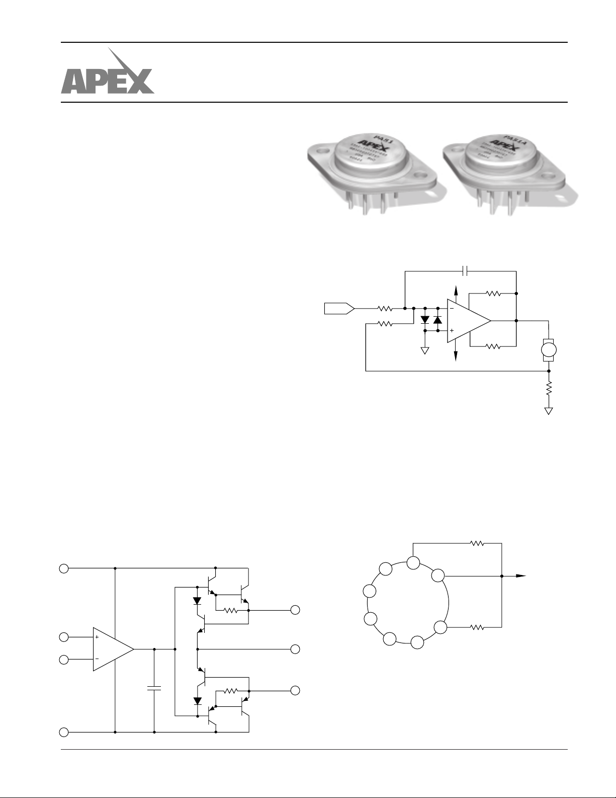
MICROTECHNOLOGY
HTTP://WWW.APEXMICROTECH.COM (800) 546-APEX (800) 546-2739
FEATURES
• WIDE SUPPLY RANGE — ±10 to ±40V
• HIGH OUTPUT CURRENT — ±10A Peak
• SECOND SOURCEABLE — OPA501, 8785
• CLASS “C” OUTPUT — Low Cost
• LOW QUIESCENT CURRENT — 2.6mA
APPLICATIONS
POWER OPERATIONAL AMPLIFIERS
PA51 • PA51A
• DC SERVO AMPLIFIER
• MOTOR/SYNCHRO DRIVER
• VALVE AND ACTUATOR CONTROL
• DC OR AC POWER REGULATOR
DESCRIPTION
The PA51 and PA51A are high voltage, high output current
operational amplifiers designed to drive resistive, inductive
and capacitive loads. Their complementary common emitter
output stage is the simple class C type optimized for low
frequency applications where crossover distortion is not critical. These amplifiers are not recommended for audio, transducer or deflection coil drive circuits. The safe operating area
(SOA) is fully specified and can be observed for all operating
conditions by selection of user programmable current limiting
resistors. Both amplifiers are internally compensated for all
gain settings. For continuous operation under load, mounting
on a heatsink of proper rating is recommended. Do not use
isolation washers!
This hybrid integrated circuit utilizes thick film conductors,
ceramic capacitors and semiconductor chips to maximize
reliability, minimize size and give top performance. Ultrasonically bonded aluminum wires provide reliable interconnections at all operating temperatures. The 8-pin TO-3 package is
electrically isolated and hermetically sealed. The use of compressible thermal washers and/or improper mounting torque
will void the product warranty. Please see “General Operating
Considerations”.
TYPICAL APPLICATION
C1
R3
.1 Ω
R4
.1 Ω
0/6A
IN
M
R5
.5 Ω
0/+5V
DAC
+10V
R1
4.16K
R2
2.5K
MOTOR CURRENT IS A FUNCTION OF V
PROGRAMMABLE TORQUE CIRCUIT
PA51
–28V
The linear relationship of torque output to current input of the
modern torque motor makes this simple control circuit ideal for
many material processing and testing applications. The sense
resistor develops a feedback voltage proportional to motor
current and the small signal properties of the Power Op Amp
insure accuracy. With this closed loop operation, temperature
induced impedance variations of the motor winding are automatically compensated.
EXTERNAL CONNECTIONS
R
EQUIVALENT SCHEMATIC
3
Q1A
Q3
4
A1
5
Q4
C1
Q6A
6
APEX MICROTECHNOLOGY CORPORATION • TELEPHONE (520) 690-8600 • FAX (520) 888-3329 • ORDERS (520) 690-8601 • EMAIL prodlit@apexmicrotech.com
Q1B
2
1
8
Q6B
+IN
–IN
+V
4
5
S
–V
3
S
TOP VIEW
6
2
7
N.C.
CL+
OUT
1
8
CL–
CL+
OUTPUT
R
CL–
PA51 • PA51A
ABSOLUTE MAXIMUM RATINGS
SPECIFICATIONS
ABSOLUTE MAXIMUM RATINGS
SUPPLY VOLTAGE, +VS to –V
OUTPUT CURRENT, within SOA 10A
S
80V
POWER DISSIPATION, internal 97W
INPUT VOLTAGE, differential ±VS –3V
INPUT VOLTAGE, common mode ±V
TEMPERATURE, junction
1
S
200°C
TEMPERATURE, pin solder -10s 300°C
TEMPERATURE RANGE, storage –65 to +150°C
OPERATING TEMPERATURE RANGE, case –55 to +125°C
SPECIFICATIONS
PARAMETER TEST CONDITIONS
PA51
2, 5
MIN TYP MAX MIN TYP MAX UNITS
PA51A
INPUT
OFFSET VOLTAGE, initial TC = 25°C ±5 ±10 ±2 ±5mV
OFFSET VOLTAGE, vs. temperature Full temperature range ±10 ±65 * ±40 µV/°C
OFFSET VOLTAGE, vs. supply TC = 25°C ±35 * µV/V
OFFSET VOLTAGE, vs. power TC = 25°C ±20 * µV/W
BIAS CURRENT, initial TC = 25°C ±15 ±40 * ±20 nA
BIAS CURRENT, vs. temperature Full temperature range ±.05 * nA/°C
BIAS CURRENT, vs. supply TC = 25°C ±.02 * nA/V
OFFSET CURRENT, initial TC = 25°C ±5 ±12 ±2 ±3nA
OFFSET CURRENT, vs. temperature Full temperature range ±.01 * nA/°C
INPUT IMPEDANCE, common mode TC = 25°C 250 * MΩ
INPUT IMPEDANCE, differential TC = 25°C10*MΩ
INPUT CAPACITANCE TC = 25°C3*pF
COMMON MODE VOLTAGE RANGE3Full temperature range ±VS–6 ±VS–3** V
COMMON MODE REJECTION, DC
3
TC = 25°C, VCM = ±VS –6V 70 110 80 * dB
GAIN
OPEN LOOP GAIN at 10Hz Full temp. range, full load 94 115 * * dB
GAIN BANDWIDTH PRODUCT @ 1MHz TC = 25°C, full load 1 * MHz
POWER BANDWIDTH TC = 25°C, IO = 8A, VO = 40V
PHASE MARGIN Full temperature range 45 * °
PP
10 16 * * kHz
OUTPUT
VOLTAGE SWING
VOLTAGE SWING
VOLTAGE SWING
3
3
3
TC = 25°C, IO = 10A ±VS–8 ±VS–5** V
Full temp. range, IO = 4A ±VS–6 ±VS–4** V
Full temp. range, IO = 68mA ±VS–6* V
CURRENT TC = 25°C ±10 * A
SETTLING TIME to .1% TC = 25°C, 2V step 2 * µs
SLEW RATE TC = 25°C, RL = 6Ω 1.0 2.6 * * V/µs
CAPACITIVE LOAD, unity gain Full temperature range 1.5 * nF
CAPACITIVE LOAD, gain > 4 Full temperature range SOA *
POWER SUPPLY
VOLTAGE Full temperature range ±10 ±28 ±36 * ±34 ±40 V
CURRENT, quiescent TC = 25°C 2.6 10 * * mA
THERMAL
RESISTANCE, AC, junction to case
4
F > 60Hz 1.0 1.2 * * °C/W
RESISTANCE, DC, junction to case F < 60Hz 1.5 1.8 * * °C/W
RESISTANCE, junction to air 30 * °C/W
TEMPERATURE RANGE, case Meets full range specifications –25 +85 –55 +125 °C
NOTES: * The specification of PA51A is identical to the specification for PA51 in applicable column to the left.
1. Long term operation at the maximum junction temperature will result in reduced product life. Derate internal power dissipation
to achieve high MTTF.
2. The power supply voltage specified under the TYP rating applies unless otherwise noted as a test condition.
3. +VS and –VS denote the positive and negative supply rail respectively. Total VS is measured from +VS to –VS.
4. Rating applies if the output current alternates between both output transistors at a rate faster than 60Hz.
5. Full temperature range specifications are guaranteed but not 100% tested.
CAUTION
APEX MICROTECHNOLOGY CORPORATION • 5980 NORTH SHANNON ROAD • TUCSON, ARIZONA 85741 • USA • APPLICATIONS HOTLINE: 1 (800) 546-2739
The internal substrate contains beryllia (BeO). Do not break the seal. If accidentally broken, do not crush, machine, or
subject to temperatures in excess of 850°C to avoid generating toxic fumes.

TYPICAL PERFORMANCE
GRAPHS
PA51 • PA51A
100
POWER DERATING
80
60
40
PA51
20
0
0 25 50 75 100 125
INTERNAL POWER DISSIPATION, P(W)
120
100
(dB)
OL
80
TEMPERATURE, T (°C)
SMALL SIGNAL RESPONSE
PA51A
60
40
20
0
OPEN LOOP GAIN, A
–20
10 1K 10K .1M 1M
1 100 10M
FREQUENCY, F (Hz)
150
OUTPUT VOLTAGE SWING
5.5
5.0
= –25°C
C
4.5
4.0
3.5
3.0
2.5
VOLTAGE DROP FROM SUPPLY (V)
T
O
+V
= 25 to 85
C
T
O
+V
02 8
°C
= –25 to 85°C
C
T
O
–V
46
OUTPUT CURRENT, I
PHASE RESPONSE
0
–30
–60
–90
–120
PHASE, (°)ϕ
–150
–180
–210
10 10K 1M
0 100 .1M 10M
1K
FREQUENCY, F (Hz)
7
6
5
LIM
CURRENT LIMIT
R = .12CLΩ
4
3
2
R = 0.3CLΩ
CURRENT LIMIT, I (A)
1
0
025 75
10
(A)
O
-25 50 100
CASE TEMPERATURE, T (°C)
C
125
POWER RESPONSE
70
PP
50
O
36
26
19
13
9.7
OUTPUT VOLTAGE, V (V )
7
10K 20K 50K .1M
FREQUENCY, F (Hz)
RL = 3 Ω
30K
VS = ±40V
RL = 8 Ω
70K
PULSE RESPONSE
8
GAIN = +1 RL = 5 Ω
6
(V)
O
4
2
0
–2
–4
OUTPUT VOLTAGE, V
–6
–8
HARMONIC DISTORTION
10
VS = ±36V
R
L
3
GAIN = 10
1
.3
.1
DISTORTION (%)
.03
.01
30 300 1K 30K
410
6
802
TIME, (µs)
= 4
Ω
= .1W
O
P
= 5W
O
P
= 50W
O
P
100 3K 10K
FREQUENCY, F (Hz)
12
COMMON MODE REJECTION
120
100
80
60
40
20
0
10 100 1K 10K .1M 1M
1
COMMON MODE REJECTION, CMR (dB)
(X)
Q
1.6
FREQUENCY, F (Hz)
QUIESCENT CURRENT
1.4
1.2
1.0
T
C
.8
T
= 125
T
C
= 125
= -55°C
C
°C
°C
.6
.4
30 40 50 60 70
20 80
TOTAL SUPPLY VOLTAGE, V
NORMALIZED QUIESCENT CURRENT, I
(V)
S
2.5
(X)
B
BIAS CURRENT
2.2
1.9
1.6
1.3
1
.7
NORMALIZED BIAS CURRENT, I
-50
-25 0 25 50 75 100 125
CASE TEMPERATURE, T
C
(°C)
INPUT NOISE
100
√
70
N
50
40
30
20
10
INPUT NOISE VOLTAGE, V (nV/ Hz)
10 1K
100
FREQUENCY, F (Hz)
10K
.1M
APEX MICROTECHNOLOGY CORPORATION • TELEPHONE (520) 690-8600 • FAX (520) 888-3329 • ORDERS (520) 690-8601 • EMAIL prodlit@apexmicrotech.com

PA51 • PA51A
GENERAL
Please read Application Note 1 "General Operating Considerations" which covers stability, supplies, heat sinking, mounting, current limit, SOA interpretation, and specification interpretation. Visit www.apexmicrotech.com for design tools that
help automate tasks such as calculations for stability, internal
power dissipation, current limit and heat sink selection. The
"Application Notes" and "Technical Seminar" sections contain
a wealth of information on specific types of applications.
Package outlines, heat sinks, mounting hardware and other
accessories are located in the "Packages and Accessories"
section. Evaluation Kits are available for most Apex product
models, consult the "Evaluation Kit" section for details. For the
most current version of all Apex product data sheets, visit
www.apexmicrotech.com.
SAFE OPERATING AREA (SOA)
The output stage of most power amplifiers has three distinct
limitations:
1. The current handling capability of the transistor geometry
and the wire bonds.
2. The second breakdown effect which occurs whenever the
simultaneous collector current and collector-emitter voltage
exceeds specified limits.
3. The junction temperature of the output transistors.
10
7.0
5.0
SS
3.0
2.0
1.5
1.0
0.7
0.5
THERMAL
T = 85
C
T = 125
C
T = 25
C
°C
°C
°C
t = 1ms
t = 5ms
steady state
OPERATING
CONSIDERATIONS
1. Under transient conditions, capacitive and dynamic* inductive loads up to the following maximums are safe:
CAPACITIVE LOAD INDUCTIVE LOAD
±V
40V 400µF 200µF 11mH 4.3mH
35V 800µF 400µF 20mH 5.0mH
30V 1,600µF 800µF 35mH 6.2mH
25V 5.0mF 2.5mF 50mH 15mH
20V 10mF 5.0mF 400mH 20mH
15V 20mF 10mF ** 100mH
* If the inductive load is driven near steady state conditions,
allowing the output voltage to drop more than 8V below the
supply rail with I
I
LIM
should be capacitively coupled or the current limit must be
lowered to meet SOA criteria.
** Second breakdown effect imposes no limitation but thermal
limitations must still be observed.
2. The amplifier can handle any EMF generating or reactive
load and short circuits to the supply rail or shorts to common
if the current limits are set as follows at T
These simplified limits may be exceeded with further analysis
using the operating conditions for a specific application.
I
S
= 5A I
LIM
= 10A I
LIM
= 10A or 15V below the supply rail with
LIM
= 5A I
LIM
= 10A
LIM
= 5A while the amplifier is current limiting, the inductor
= 85°C.
C
±V
SHORT TO ±V
S
C, L, OR EMF LOAD COMMON
S
SHORT TO
45V 0.1A 1.3A
40V 0.2A 1.5A
35V 0.3A 1.6A
30V 0.5A 2.0A
25V 1.2A 2.4A
20V 1.5A 3.0A
15V 2.0A 4.0A
0.3
OUTPUT CURRENT FROM +V OR –V (A)
0.2
710
515203040507080
SUPPLY TO OUTPUT DIFFERENTIAL VOLTAGE V –V (V)
SO
The SOA curves combine the effect of of all limits for this
Power Op Amp. For a given application, the direction and
magnitude of the output current should be calculated or
measured and checked against the SOA curves. This is simple
for resistive loads but more complex for reactive and EMF
generating loads. The following guidelines may save exten-
3.The output stage is protected against transient flyback.
However, for protection against sustained, high energy
flyback, external fast-recovery diodes should be used.
CURRENT LIMIT
Proper operation requires the use of two current limit
resistors, connected as shown in the external connection
diagram. The minimum value for R
optimum reliability it should be set as high as possible. Refer
to the “General Operating Considerations” section of the
handbook for current limit adjust details.
is .06 ohm, however for
CL
sive analytical efforts.
This data sheet has been carefully checked and is believed to be reliable, however, no responsibility is assumed for possible inaccuracies or omissions. All specifications are subject to change without notice.
PA51U REV. L FEBRUARY 2000 © 2000 Apex Microtechnology Corp.
 Loading...