

MICROTECHNOLOGY
FEATURES
POWER OPERATIONAL AMPLIFIERS
PA50 • PA50A
HTTP://WWW.APEXMICROTECH.COM (800) 546-APEX (800) 546-2739
• HIGH INTERNAL DISSIPATION — 400 Watts
• HIGH CURRENT — 40A Continuous, 100A PEAK
• HIGH SLEW RATE — 50V/µs
• OPTIONAL BOOST VOLTAGE INPUTS
APPLICATIONS
• SEMI-CONDUCTOR TESTING
DESCRIPTION
The PA50 is a MOSFET power operational amplifier that
extends the performance limits of power amplifiers in slew rate
and power bandwidth, while maintaining high current and
power dissipation ratings.
Boost voltage inputs allow the small signal portion of the
amplifier to operate at a higher voltage than the high current
output stage. The amplifier is then biased to achieve close
linear swings to the supply rails at high currents for extra
efficient operation.
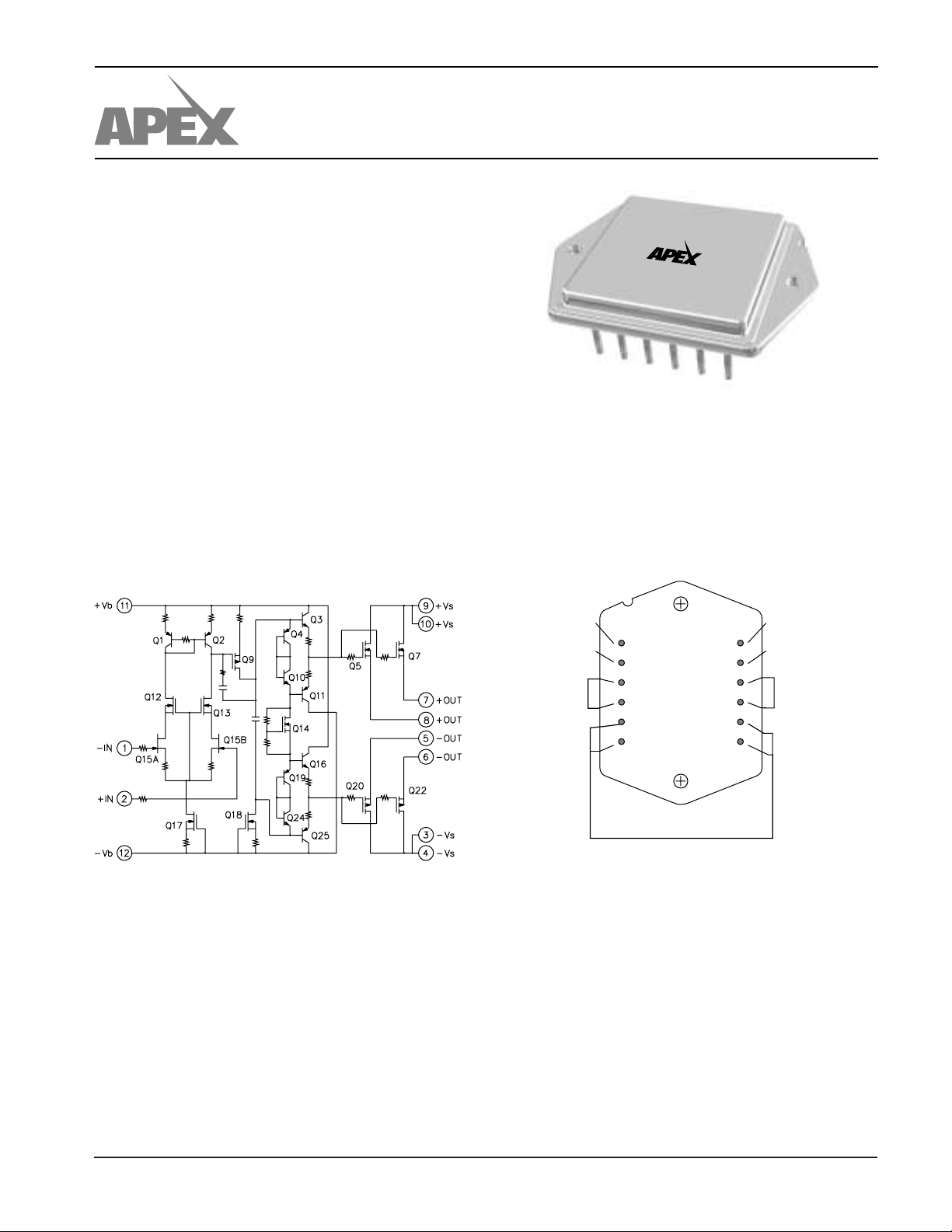
EQUIVALENT SCHEMATIC
PA
50A
∆
U
S
ABe
T
O
E
9
4
9
3
1
1
The JEDEC MO-127 12-pin Power Dip™ package (see
Package Outlines) is hermetically sealed and isolated from the
internal circuits. The use of compressible thermal washers
and/or improper mounting torque will void the product warranty. Please see “General Operating Considerations”.
EXTERNAL CONNECTIONS
-V
–IN
+IN
-V
-V
-OUT
-OUT
1
2
s
s
3
TOP
TOP
VIEW
VIEW
4
5
6
12
11
10
9
8
7
b
b
+V
+V
s
+V
s
+OUT
+OUT
APEX MICROTECHNOLOGY CORPORATION • TELEPHONE (520) 690-8600 • FAX (520) 888-3329 • ORDERS (520) 690-8601 • EMAIL prodlit@apexmicrotech.com

P A50 • P A50A
ABSOLUTE MAXIMUM RATINGS
SPECIFICATIONS
ABSOLUTE MAXIMUM RATINGS
SUPPLY VOLTAGE, +VS to –V
BOOST VOLTAGE, +Vb to -V
OUTPUT CURRENT, within SOA 100A
S
b
100V
130V
POWER DISSIPATION, internal 400W
INPUT VOLTAGE, differential ±20V
INPUT VOLTAGE, common mode ±V
TEMPERATURE, pin solder - 10s 300°C
TEMPERATURE, junction
2
b
175°C
TEMPERATURE, storage –65 to +150°C
OPERATING TEMPERATURE RANGE, case –55 to +125°C
SPECIFICATIONS
PARAMETER TEST CONDITIONS
1
MIN TYP MAX MIN TYP MAX UNITS
PA50APA50
INPUT
OFFSET VOLTAGE, initial 5 10 2 5 mV
OFFSET VOLTAGE, vs. temperature Full temperature range 20 50 * * µV/°V
OFFSET VOLTAGE, vs. supply 10 30 * * µV/V
BIAS CURRENT, initial 10 50 * * pA
BIAS CURRENT vs. supply .01 * pA/V
OFFSET CURRENT, initial 10 50 * * pA
INPUT IMPEDANCE, DC 10" * Ω
IMPUT CAPACITANCE 13 * pF
COMMON MODE VOLTAGE RANGE Full temperature range ±Vb 12 * V
±
COMMON MODE REJECTION,DC Full temp, range, VCM= ±20V 90 100 * * dB
INPUT NOISE 100KHZ BW, Rs=1KΩ 10 * µVrms
GAIN
OPEN LOOP,@ 15Hz Full temperature range 94 102 * * dB
GAIN BANDWIDTH PRODUCT RL=10Ω 3 * MHz
POWER BANDWIDTH RL=4Ω, Vo=80V
Full temperature range
, Av=-10 400 * kHz
P-P
OUTPUT
VOLTAGE SWING Io=40A ±VS 9.5 ±VS 8.7 * * V
VOLTAGE SWING, PA50 ±V
VOLTAGE SWING, PA50A ±V
CURRENT, peak 3ms 10% Duty Cycle 100 * A
=±VS±10V, Io=40A ±VS 5.8 ±VS 5.0 V
BOOST
=±VS±10V, Io=50A ±VS 5.8 ±VS 5.0 V
BOOST
±
±
±
±
± ±
SETTLING TIME TO.1% AV= -10,10V STEP,RL=4Ω 1*µs
SLEW RATE AV=-10 50 * V/µs
RESISTANCE IO=0, NO LOAD, 2MHZ 2.5 * Ω
POWER SUPPLY
VOLTAGE, ±V
VOLTAGE, ±V
CURRENT,quiescent, boost supply 26 32 * * mA
BOOST
S
Full temperature range ±12 ±15 ±65 * * * V
Full temperature range ±3 ±50 * * V
CURRENT, quiescent, total 30 36 * * mA
THERMAL
RESISTANCE,AC,junction to case3Full temperature range, F>60HZ .2 .25 * * °C/W
RESISTANCE,DC,junction to case Full temperature range, F>60HZ .25 .31 * * °C/W
RESISTANCE, junction to air Full temperature range 12 * °C/W
TEMPERATURE RANGE, case Meets full range specification -25 85 * * °C
NOTES: * The specification of PA50A is identical to the specification for PA50 in applicable column to the left
1. Unless otherwise noted: TC = 25°C, DC input specifications are ± value given. Power supply voltage is typical rating.
±V
= ±VS.
BOOST
2. Long term operation at the maximum junction temperature will result in reduced product life. Derate internal power dissipation
to achieve high MTTF. For guidance, refer to the heatsink data sheet.
3. Rating applies if the output current alternates between both output transistors at a rate faster than 60 Hz.
CAUTION
The PA50 is constructed from MOSFET transistors. ESD handling procedures must be observed.
The internal substrate contains beryllia (BeO). Do not break the seal. If accidentally broken, do not crush, machine, or
subject to temperatures in excess of 850°C to avoid generating toxic fumes.
APEX MICROTECHNOLOGY CORPORATION • 5980 NORTH SHANNON ROAD • TUCSON, ARIZONA 85741 • USA • APPLICATIONS HOTLINE: 1 (800) 546-2739

TYPICAL PERFORMANCE
GRAPHS
P A50 • PA50A
500
POWER DERATING
400
T = T
300
C
200
100
0
0 25 50 75 100
INTERNAL POWER DISSIPATION, P(W)
120
TEMPERATURE, T (°C)
SMALL SIGNAL GAIN
80
40
0
RL = 4Ω
OPEN LOOP GAIN RESPONSE, A(dB)
1 100 1K 10K 100K 1M
10 10M
FREQUENCY,Ff (Hz)
POWER SUPPLY REJECTION
100
80
60
40
20
0
100 1K 10M
10
POWER SUPPLY REJECTION, PSR (dB)
SMALL SIGNAL PHASE
0
10K 100K 1M
FREQUENCY F (Hz)
RL = 4Ω
–45
–90
–135
OPEN LOOP PHASE, (°)Φ
–180
100 10M1 10 1K 10K 100K 1M
FREQUENCY, F (Hz)
OUTPUT VOLTAGE SWING
(V)
O
10
–V
S
8
S
T
6
S
O
O
V = V
B
4
+ 10V
2
0
010 304050
OUTPUT CURRENT, I (A)
VOLTAGE DROP FROM SUPPLY, V
100
)
PP
O
POWER RESPONSE
90
80
70
60
V = V
20
S
ST
O
O
B
O
50
40
30
OUTPUT VOLTAGE, V (V
20
100K
FREQUENCY, F (Hz)
1M
COMMON MODE REJECTION
100
80
60
40
20
0
10
COMMON MODE REJECTION, CMR (dB)
FREQUENCY, F (Hz)
1M100 1K 10K 100K
Q
1.125
QUIESCENT CURRENT
±VS = ±V
B
1.1
1.075
1.05
1.025
1
20 100
40 60 80
TOTAL SUPPLY VOLTAGE, V (V)
NORMALIZED QUIESCENT CURRENT, I (X)
S
SAFE OPERATING AREA
100
10
DC Tc = 125
t = 1m
t = 10ms
DC Tc = 25
DC Tc = 85
°C
s
°C
°C
1
OUTPUT CURRENT, (A)
0.1
10
SUPPLY TO OUTPUT DIFFERENTIAL, (V)
1001
APEX MICROTECHNOLOGY CORPORATION • TELEPHONE (520) 690-8600 • FAX (520) 888-3329 • ORDERS (520) 690-8601 • EMAIL prodlit@apexmicrotech.com

PA50 • P A50A
GENERAL
Please read Application Note 1 "General Operating Considerations" which covers stability, supplies, heat sinking, mounting, current limit, SOA interpretation, and specification interpretation. Visit www.apexmicrotech.com for design tools that
help automate tasks such as calculations for stability, internal
power dissipation, current limit; heat sink selection; Apex’s
complete Application Notes library; Technical Seminar Workbook; and Evaluation Kits.
CURRENT LIMIT
There is no internal circuit provision for current limit in the
PA50. However, the PA50 circuit board in the PA50 evaluation
kit does provide a means whereby the output current can be
sensed. An external circuit current limit can thereby be implemented if needed. See EK27 data sheet for more details.
BOOST OPERATION
With the V
amplifier are operated at higher supply voltages than the
amplifier’s high current output stage. +V
–V
(pin 12) are connected to the small signal circuitry of
BOOST
the amplifier. +V
the high current output stage. An additional 10V on the V
pins is sufficient to allow the small signal stages to drive the
output transistors into saturation and improve the output
voltage swing for extra efficient operation when required.
When close swings to the supply rails is not required the
+V
and +VS pins must be strapped together as well as the
BOOST
–V
and –VS pins. The boost voltage pins must not be at a
BOOST
voltage lower than the V
feature the small signal stages of the
BOOST
(pin 11) and
BOOST
(pin 9,10) and –VS (pin 3,4) are connected to
S
pins.
S
BOOST
OPERATING
CONSIDERATIONS
COMPENSATION
Compensation is internally fixed for a gain of 3 or more and
is not adjustable by the user. The PA50 therefore is not unity
gain stable.
POWER SUPPLY BYPASSING
Proper and sufficient power supply bypassing is crucial to
proper operation of the PA50. Bypass the +Vb and -Vb supply
pins with a minimum .1µF ceramic capacitors directly at the
supply pins. On the +Vs and -Vs pins use a combination of
ceramic and electrolytic capacitors. Use 1µF ceramic capacitors and an electrolytic capacitor at least 10µF for each amp of
output current required.
This data sheet has been carefully checked and is believed to be reliable, however, no responsibility is assumed for possible inaccuracies or omissions. All specifications are subject to change without notice.
APEX MICROTECHNOLOGY CORPORATION • 5980 NORTH SHANNON ROAD • TUCSON, ARIZONA 85741 • USA • APPLICATIONS HOTLINE: 1 (800) 546-2739
PA50U REV A JANUARY 2001 © 2001 Apex Microtechnology Corp.
 Loading...