

HIGH VOLTAGE POWER OPERATIONAL AMPLIFIER
MICROTECHNOLOGY
HTTP://WWW.APEXMICROTECH.COM (800) 546-APEX (800) 546-2739
PRELIMINARY
FEATURES
• MONOLITHIC MOS TECHNOLOGY
• LOW COST
• HIGH VOLTAGE OPERATION—350V
• LOW QUIESCENT CURRENT—2mA
• NO SECOND BREAKDOWN
• HIGH OUTPUT CURRENT—120 mA PEAK
APPLICATIONS
• TELEPHONE RING GENERATOR
• PIEZO ELECTRIC POSITIONING
• ELECTROSTATIC TRANSDUCER & DEFLECTION
• DEFORMABLE MIRROR FOCUSING
DESCRIPTION
The PA40 is a high voltage monolithic MOSFET operational
amplifi er achieving performance features previously found
only in hybrid designs while increasing reliability. Inputs are
protected from excessive common mode and differential
mode voltages. The saf e operating area (SOA) has no second
breakdown limitations. External compensation provides the
user fl exibility in choosing optimum gain and bandwidth
for the application.
The PA40 is packaged in Apex's 7 LEAD TO220 package.
The metal back of the package is tied to –Vs. The 15 mil
minimum spacing of the TO220 package is adequate to
stand-off the 350V rating of the PA40. The user must insure
that a minimum of 11 mils spacing is maintained between
pins for the circuit board artwork. If spacing is less than 11
mils, the voltage must be derated.
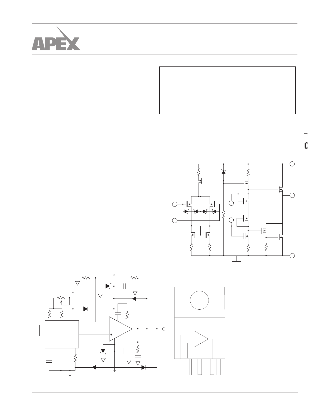
TYPICAL APPLICATION
140V
IN6300A
15V
2.5K + 15
100K2.67K
.22
PA40
PA40 GRAPHIC HERE
The PA40 is set for a gain of 38.5 boosting the 2.33V signal
to 90V. The recommended compensation for gains above 30
is used. If capacitiv e loading is at least 330pF at all times, the
recommended snubber network may be omitted.
EQUIVALENT SCHEMATIC
3
+V
I
OUT
–V
12
S
5
S
Q1
Q5Q4
1
–IN
D2 D3 D4 D5
2
+IN
Q11
Q12
EXTERNAL CONNECTIONS
D1
7
COMP
COMP
8
SUB
Q6
Q8
Q13
Q2
Q3
Q10
Q14
MUR130
–140V
3.3pF
.22
2.2K
27
100
330pf
MUR130
90Vrms
1234 567
-IN
+VS
-VS
OUT
COMP
COMP
+ IN
PHASE COMPENSATION
Gain C
1 18pF 2.2K
10 10pF 2.2K
30 3.3pF 2.2K
R
C
C
10K 10K
7
ICL8038
8
*
* 1.5 µF @ 16Hz
1.2 µF @ 20Hz
1110
54
–15V
MUR120
6
2
IN6300A
82K
MUR120
Telephone Ring Generator
APEX MICROTECHNOLOGY CORPORATION • TELEPHONE (520) 690-8600 • FAX (520) 888-3329 • ORDERS (520) 690-8601 • EMAIL prodlit@apexmicrotech.com
1
PA40
ABSOLUTE MAXIMUM RATINGS
SPECIFICATIONS
ABSOLUTE MAXIMUM RATINGS
SUPPLY VOLT A GE, +VS to –V
OUTPUT CURRENT, continuous within SOA 60 mA
S
350V
OUTPUT CURRENT, peak 120 mA
POWER DISSIPATION, continuous @ TC = 25°C 18W
INPUT VOLTAGE, differential ±16 V
INPUT VOLTAGE, common mode ±V
TEMPERATURE, pin solder – 10 sec 220°C
S
TEMPERATURE, junction2 150°C
TEMPERATURE, storage –65 to +150°C
TEMPERATURE RANGE, powered (case) –40 to +125°C
SPECIFICATIONS
PA44
PARAMETER TEST CONDITIONS1 MIN TYP MAX UNITS
INPUT
OFFSET VOLTAGE, initial 15 30 mV
OFFSET VOLT A GE, vs. temperature
4
Full temperature range 70 130 µV/°C
OFFSET VOLTAGE, vs supply 20 32 µV/V
OFFSET VOLTAGE, vs time 75 µV kh
BIAS CURRENT, initial 50 2
00
pA
BIAS CURRENT, vs supply 2 20 pA/V
OFFSET CURRENT, initial 50 200 pA
INPUT IMPEDANCE, DC 101
1
INPUT CAPACITANCE 5 pF
COMMON MODE, voltage range ±VS–
COMMON MODE REJECTION, DC VCM
NOISE, broad band 10kHz BW, RS
NOISE, low frequency 1-10 Hz 1
±90V DC 84 94 dB
=
1K 5
=
2 V
1
0
µV p-p
10
µV RMS
GAIN
OPEN LOOP at 15Hz RL =
BANDWIDTH, open loop 1.6 MHz
POWER BANDWIDTH CC =
PHASE MARGIN Full temperature range 60 °
5K 94 106 dB
0pf, 280V p-p 26 kHz
1
OUTPUT
VOLTAGE SWING IO =
CURRENT, peak
5
0mA ±VS–12
4
±VS–10
V
120 mA
CURRENT, continuous 60 mA
SETTLING TIME to .1% CC =
SLEW RATE CC =
CAPACITIVE LOAD AV =
RESISTANCE6, n
RESISTANCE6, 20
POWER SUPPLY
VOLT AGE
o
load RCL = 0 150
m
A load RCL =
3
See Note 3 ±50 ±150 ±175 V
0pF, 10V step, AV = –10 12 µs
1
PEN 40 V/µs
O
1 10 nF
+
0
25
CURRENT, quiescent 1.6 2.0 mA
THERMAL
ANCE, AC junction to case F > 6
RESIST
ANCE, DC junction to case F < 6
RESIST
0Hz 3.7 4.3 °C/W
0Hz 5.6 6.8 °C/W
RESISTANCE, junction to air Full temperature range 74 °C/W
TEMPERATURE RANGE, case Meets full range specifi cations –25 +85 °C
NOTES: 1. Unless otherwise noted TC = 25°C, CC = 18pF, RC = 2.2K. DC input specifi cations are ± value given. Power supply voltage
is typical rating.
2. Long term operation at the maximum junction temperature will result in reduced product life. Derate internal power dissipation
to achieve high MTTF.
3. Derate maximum supply voltage .5 V/°C below case temperature of 25°C. No derating is needed above TC
4. Sample tested by wafer to 95%.
= 25°C.
5. Guaranteed but not tested.
CAUTION
The PA40 is constructed from MOSFET transistors. ESD handling procedures must be observed.
APEX MICROTECHNOLOGY CORPORATION • 5980 NORTH SHANNON ROAD • TUCSON, ARIZONA 85741 • USA • APPLICATIONS HOTLINE: 1 (800) 546-2739

TYPICAL PERFORMANCE
GRAPHS
PA40
20
POWER DERATING
T = T
C
16
12
8
4
T = T
A
0
0 25 50 75 100 125
INTERNAL POWER DISSIPATION, P(W)
120
TEMPERATURE, T (°C)
SMALL SIGNAL RESPONSE
100
CC = 3.3pF
80
60
CC = 10pF
40
CC = 18pF
20
OPEN LOOP GAIN, A(dB)
0
–20
10 1K 10K .1M 1M
1 100 10M
FREQUENCY, F (Hz)
HARMONIC DISTORTION
1.0
AV = 20
.6
= 3.3pf
C
.4
C
R
= 2K Ω
L
.2
.1
VO = 30V
.06
.04
.02
DISTORTION, (%)
.01
.006
.004
.002
100 10K
PP
VO = 180V
VO = 60V
3K 100K
PP
30K200 1K
FREQUENCY, F (Hz)
COMMON MODE REJECTION
120
PHASE RESPONSE
0
–30
–60
CC = 3.3pF
CC = 10pF
–90
CC = 18pF
–120
PHASE, (°)ϕ
–150
CC = 3.3pF
–180
–210
1 100 .1M 10M
10 10K 1M
CC = 10pF
1K
FREQUENCY, F (Hz)
60
SLEW RATE
50
40
30
20
SLEW RATE, V/µs
10
0
0
42081612
COMPENSATION CAPACITANCE, C
POWER SUPPLY REJECTION
120
100
80
PP
60
–V
40
20
0
11M
POWER SUPPLY REJECTION, PSR (dB)
10 100 1K 10K .1M
FREQUENCY, F (Hz)
S
CC = 18pF
+V
S
C
(pf)
400
PP
200
O
100
80
60
40
OUTPUT VOLTAGE, V (V )
CC = 18pF
20
10K 20K .2M.1M
30K
50K .3M .5M 1M
FREQUENCY, F (Hz)
QUIESCENT CURRENT
150
130
110
90
T
70
50
100 150 300 350
NORMALIZED QUIESCENT CURRENT, (%)
TOTAL SUPPLY VOLTAGE, V
(V)
OUTPUT VOLTAGE SWING
O
18
– V
S
16
14
12
10
8
200
85°C –OUT
25°C –OUT
–
6
4
2
25°C +OUT
0
20 120
04060
OUTPUT CURRENT, I
VOLTAGE DROP FROM SUPPLY, V
RL = 10KΩ
CC = 10pF
CC = 3.3pF
= 85°C
C
= 25°C
C
T
= -25°C
T
C
250
25°C –OUT
–25°C +OUT
85°C +OUT
80
100
(mA)
O
S
(V)
POWER RESPONSE
100
80
60
40
20
0
10 10K .1M
1 100 1K 1M
COMMON MODE REJECTION, CMR (dB)
FREQUENCY, F (Hz)
APEX MICROTECHNOLOGY CORPORATION • TELEPHONE (520) 690-8600 • FAX (520) 888-3329 • ORDERS (520) 690-8601 • EMAIL prodlit@apexmicrotech.com
3

PA40
OPERATING
CONSIDERATIONS
GENERAL
Please read Application Note 1 "General Operating
Considerations" which covers stability, supplies, heat sinking,
mounting, current limit, SOA interpretation, and specifi cation
interpretation. Visit www.apexmicrotech.com for design tools
that help automate tasks such as calculations for stability,
internal power dissipation, current limit; heat sink selection;
Apex’s complete Application Notes library; Technical Seminar
Workbook; and Evaluation Kits.
INPUT PROTECTION
The PA40 inputs are protected against common mode
voltages up the supply rails and differential voltages up to
±16 volts as well as static discharge. Differential voltages
exceeding 16 volts will be clipped by the protection circuitr y.
However, if more than a few milliamps of current is available
from the overload source, the protection circuitry could be
destroyed. The protection circuitry includes 300 ohm current
limiting resistors at each input, but this may be insuffi cient
for severe overloads. It may be necessary to add external
resistors to the application circuit where severe overload
conditions are expected. Limiting input current to 1mA will
prevent damage.
STABILITY
The PA40 has suffi cient phase margin when compensated
for unity gain to be stable with capacitive loads of at least
10 nF. However, the low pass circuit created by the sumpoint
(–in) capacitance and the feedback network may add phase
shift and cause instabilities. As a general rule, the sumpoint
load resistance (input and feedback resistors in parallel)
should be 1K ohm or less at low gain settings (up to 10).
Alternatively, use a bypass capacitor across the feedback
resistor. The time constant of the feedbac k resistor and bypass
capacitor combination should match the time constant of the
sumpoint resistance and sumpoint capacitance.
The PA40 is externally compensated and performance can
be tailored to the application. Use the graphs of small signal
gain and phase response as well as the graphs for slew rate
and power response as a guide. The compensation capacitor
must be rated at 350V working voltage. The compensation
C
C
capacitor and associated resistor R
to the amplifi er pins to avoid spurious oscillation. An NPO
capacitor is recommended for compensation.
must be mounted closely
C
200
120
100
, (mA)
S
50
OR –V
S
40
30
20
10
5
4
3
OUTPUT CURRENT FROM +V
PULSE CURVES @ 10% DUTY CYCLE MAX
2
10 20 30 50 100 200 300 500
SUPPLY TO OUTPUT DIFFERENTIAL, VS -VO (V)
PA40 SOA
300mS
DC, T
DC, T
C
= 125°C
DC
C
= 85°C
200mS
SAFE OPERATING AREA (SOA)
The MOSFET output stage of this power operational
amplifi er has two distinct limitations:
1. The current handling capability of the die metallization.
2. The temperature of the output MOSFETs.
NOTE: The output stage is protected against transient
fl yback. However, f or protection against sustained, high energy
fl yback, external fast-recovery diodes should be used.
This data sheet has been carefully checked and is believed to be reliable, however, no responsibility is assumed for possible inaccuracies or omissions. All specifi cations are subject to change without notice.
APEX MICROTECHNOLOGY CORPORATION • 5980 NORTH SHANNON ROAD • TUCSON, ARIZONA 85741 • USA • APPLICATIONS HOTLINE: 1 (800) 546-2739
PA40U REV. 1 JANUARY 2001 © 2001 Apex Microtechnology Corp.
 Loading...