

POWER DUAL OPERATIONAL AMPLIFIERS
PA21/25/26 • PA21A/25A
MICROTECHNOLOGY
FEATURES
• LOW COST
• WIDE COMMON MODE RANGE —
Includes negative supply
• WIDE SUPPLY VOLTAGE RANGE
Single supply: 5V to 40V
Split supplies: ±2.5V to ±20V
• HIGH EFFICIENCY — |Vs–2.2V| at 2.5A typ
• HIGH OUTPUT CURRENT — 3A min (PA21A)
• INTERNAL CURRENT LIMIT
• LOW DISTORTION
APPLICATIONS
• HALF & FULL BRIDGE MOTOR DRIVERS
• AUDIO POWER AMPLIFIER
STEREO — 18W RMS per channel
BRIDGE — 36W RMS per package
• IDEAL FOR SINGLE SUPPLY SYSTEMS
5V — Peripherals
12V — Automotive
28V — Avionic
DESCRIPTION
The amplifiers consist of a monolithic dual power op amp
in a 8-pin hermetic TO-3 package (PA21 and PA25) and a 12pin SIP package (PA26). Putting two power op amps in one
package and on one die results in an extremely cost effective
solution for applications requiring multiple amplifiers per
board or bridge mode configurations.
The wide common mode input range includes the negative
rail, facilitating single supply applications. It is possible to
have a “ground based” input driving a single supply amplifier
with ground acting as the “second” or “bottom” supply of the
amplifier.
The output stages are also well protected. They possess
internal current limit circuits. While the device is well protected, the Safe Operating Area (SOA) curve must be observed. Proper heatsinking is required for maximum reliability.
This hybrid integrated circuit utilizes thick film (cermet)
resistors, ceramic capacitors and semiconductor chips to
maximize reliability, minimize size and give top performance.
Ultrasonically bonded aluminum wires provide reliable interconnections at all operating temperatures. The 8-pin TO-3
package is hermetically sealed and electrically isolated. The
use of compressible isolation washers voids the warranty.
The tab of the SIP12 plastic package is tied to –V
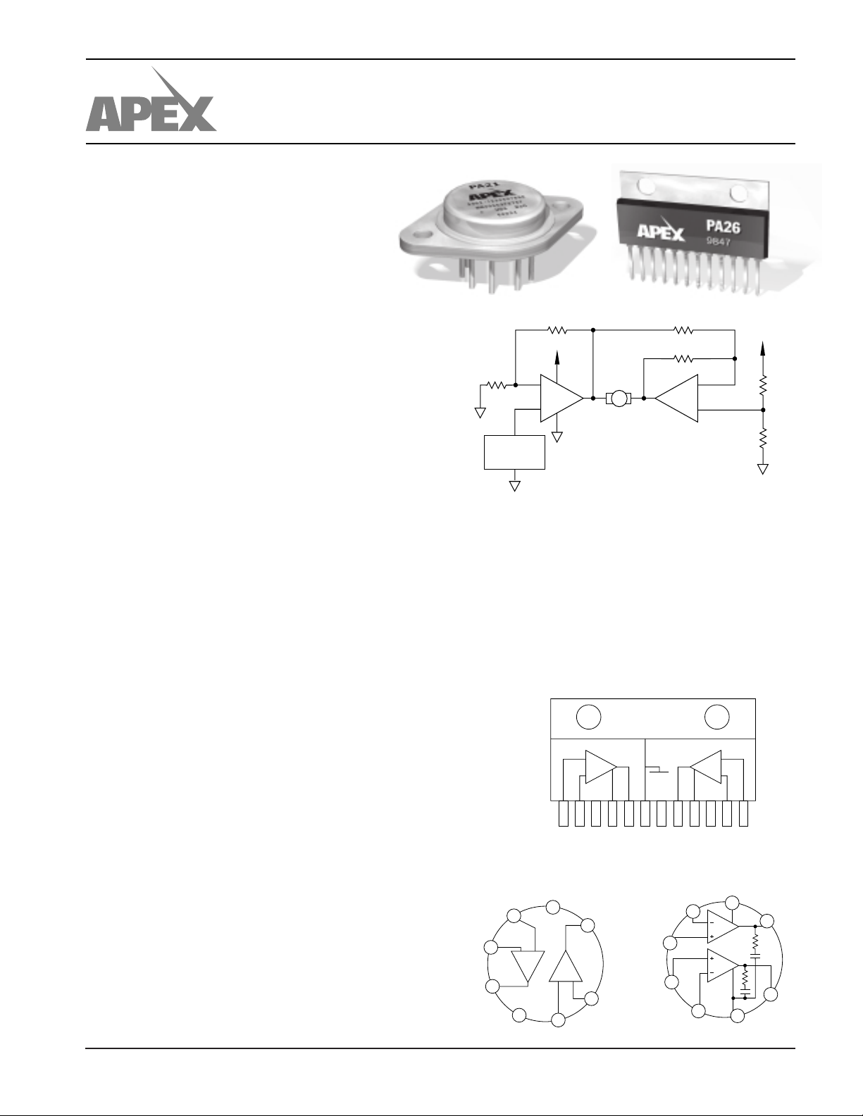
TYPICAL APPLICATION
R1 and R2 set up amplifier A in a non-inverting gain of 2.8.
Amp B is set up as a unity gain inverter driven from the output
of amp A. Note that amp B inverts signals about the reference
node, which is set at mid-supply (14V) by R5 and R6. When the
command input is 5V, the output of amp A is 14V. Since this is
equal to the reference node voltage, the output of amp B is also
14V, resulting in 0V across the motor. Inputs more positive
than 5V result in motor current flow from left to right (see Figure
1). Inputs less positive than 5V drive the motor in the opposite
direction.
HTTP://WWW.APEXMICROTECH.COM (800) 546-APEX (800) 546-2739
.
S
R1
5K
COMMAND
INPUT
0/10V
R2
9K
+28V
–
A B
+
1/2 PA21
M
R3
R4
1/2 PA21
10K
10K
+28V
–
+
R5
10K
R6
10K
FIGURE 1: BIDIRECTIONAL SPEED CONTROL FROM
A SINGLE SUPPLY
The amplifiers are especially well-suited for this application.
The extended common mode range allows command inputs
as low as 0V. Its superior output swing abilities let it drive within
2V of supply at an output current of 2A. This means that a
command input that ranges from 0V to 10V will drive a 24V
motor from full scale CCW to full scale CW at up to ±2A. A
single power op amp with an output swing capability of Vs –6
would require ±30V supplies and would be required to swing
48V p-p at twice the speed to deliver an equivalent drive.
EXTERNAL CONNECTIONS
PA26
Connect pins
3 and 10 to pin 7
and connect pins
4 and 9 to pin 6
unless special
functions are required.
+IN, A
3
–IN, A
4
– +
5
OUT, A
TOP VIEW
–V
S
6
PA25
+V
A
+IN, B
+
A
–
123456789101112
S
/+V
–IN A
+IN A
BOOST
V
S
2
OUT, B
1
B
–+
8
–IN, B
7
S
/–V
SENSE
I
SUB
S+VS
–V
OUT A
–IN, A
4
+IN, A
5
+IN, B
–IN, B
/–V
OUT B
I
3
6
+
B
–
S
SENSE
S
/+V
BOOST
V
+V
A
B
PA21
2
–V
–IN B
S
7
S
+IN B
OUT, A
1
8
OUT, B
APEX MICROTECHNOLOGY CORPORATION • TELEPHONE (520) 690-8600 • FAX (520) 888-3329 • ORDERS (520) 690-8601 • EMAIL prodlit@apexmicrotech.com
PA21/25/26 • PA21A/25A
ABSOLUTE MAXIMUM RATINGS
SPECIFICATIONS
ABSOLUTE MAXIMUM RATINGS
SUPPLY VOLTAGE, total 5V to 40V
OUTPUT CURRENT SOA
POWER DISSIPATION, internal (per amplifier) 25W
POWER DISSIPATION, internal (both amplifiers) 36W
INPUT VOLTAGE, differential ±V
INPUT VOLTAGE, common mode +VS, -VS–.5V
JUNCTION TEMPERATURE, max
1
S
150°C
TEMPERATURE, pin solder—10 sec max 300°C
TEMPERATURE RANGE, storage –65°C to 150°C
OPERATING TEMPERATURE RANGE, case –55°C to 125°C
SPECIFICATIONS
PARAMETER TEST CONDITIONS
PA21/25/26
2
MIN TYP MAX MIN TYP MAX UNITS
PA21A/PA25A
INPUT
OFFSET VOLTAGE, initial 1.5 10 .5 4 mV
OFFSET VOLTAGE, vs. temperature Full temperature range 15 10 µV/°C
BIAS CURRENT, initial 35 1000 * 250 nA
COMMON MODE RANGE Full temperature range –VS–.3 +VS–2* * V
COMMON MODE REJECTION, DC Full temperature range 60 85 * * dB
POWER SUPPLY REJECTION Full temperature range 60 80 * * dB
CHANNEL SEPARATION I
= 1A, F = 1kHz 50 68 * * dB
OUT
GAIN
OPEN LOOP GAIN Full temperature range 80 100 * * dB
GAIN BANDWIDTH PRODUCT AV = 40dB 600 * kHz
PHASE MARGIN Full temperature range 65 * °
POWER BANDWIDTH V
= 28V 13.6 * kHz
O(P-P)
OUTPUT
CURRENT, peak 2.5 3 A
CURRENT, limit 3.0 4.0 A
SLEW RATE .5 1.2 * * V/µs
CAPACITIVE LOAD DRIVE AV = 1 .22 * µF
VOLTAGE SWING Full temp. range, IO = 100mA |VS| –1.0 |VS| –0.8 * * V
VOLTAGE SWING Full temp. range, IO = 1A |VS| –1.8 |VS| –1.4 * * V
VOLTAGE SWING IO = 2.5A (PA21, 25) |VS| –3.0 |VS| –2.8 V
VOLTAGE SWING IO = 3.0A (PA21A, PA25A) |VS| –4.0 |VS| –3.5 V
POWER SUPPLY
VOLTAGE, V
CURRENT, quiescent, total 45 90 * * mA
3
SS
4
5
30 40 * * * V
THERMAL
RESISTANCE, junction to case
DC, single amplifier 5.0 * °C/W
DC, both amplifiers
AC, single amplifier 3.7 °C/W
AC, both amplifiers
5
5
3.4 * °C/W
2.4 °C/W
RESISTANCE, junction to air 30 * °C/W
TEMPERATURE RANGE, case Meets full range specifications –25 85 –25 85 °C
NOTES: * The specification of PA21A/PA25A is identical to the specification for PA21/PA25 in applicable column to the left.
1. Long term operation at the maximum junction temperature will result in reduced product life. Derate internal power dissipation
to achieve high MTTF.
2. Unless otherwise noted, the following conditions apply: ±V
3. +VS and –VS denote the positive and negative supply rail respectively. VSS denotes the total rail-to-rail supply voltage.
= ±15V, TC = 25°C.
S
4. Current limit may not function properly below VSS = 6V, however SOA violations are unlikely in this area.
5. Rating applies when power dissipation is equal in the two amplifiers.
CAUTION
The internal substrate contains beryllia (BeO). Do not break the seal. If accidentally broken, do not crush, machine, or
subject to temperatures in excess of 850°C to avoid generating toxic fumes. (PA21 and PA25 only. PA26 does not contain
BeO).
APEX MICROTECHNOLOGY CORPORATION • 5980 NORTH SHANNON ROAD • TUCSON, ARIZONA 85741 • USA • APPLICATIONS HOTLINE: 1 (800) 546-2739

TYPICAL PERFORMANCE
GRAPHS
PA21/25/26 • PA21A/25A
40
POWER DERATING
35
30
25
BOTH
AMPLIFIERS
20
15
SINGLE
AMPLIFIER
10
5
0
0 25 50 75 100 125
INTERNAL POWER DISSIPATION, P(W)
100
TEMPERATURE, T (°C)
SMALL SIGNAL RESPONSE
80
60
40
20
0
OPEN LOOP GAIN, A (dB)
–20
1 100 1M
10 1K 10K 100K
FREQUENCY, F (Hz)
150
1.75
B
BIAS CURRENT
1.5
1.25
1.0
.75
.5
.25
NORMALIZED BIAS CURRENT, I (X)
–50 0 100
–25 25 50 75
CASE TEMPERATURE, T (°C)
PHASE RESPONSE
0
–30
–60
–90
–120
PHASE, (°)ϕ
–150
–180
–210
0 100 .1M
10 10K 1M
1K
FREQUENCY, F (Hz)
80
75
70
CROSSTALK
AMP 1
I = 1A
OUT
AV = –100
65
AMP 2
60
I = 0
CROSSTALK (dB)
OUT
AV = –100
55
50
125
C
10 1K
100
FREQUENCY, F (Hz)
10K
20K
POWER RESPONSE
50
40
PP
30
O
25
20
15
10
|+V | + |–V | = 40V
OUTPUT VOLTAGE, V (V )
SS
5
1K 100K
10K
FREQUENCY, F (Hz)
POWER SUPPLY REJECTION
89
86
83
80
77
74
71
69
66
63
60
0 10K
POWER SUPPLY REJECTION, PSR (dB)
HARMONIC DISTORTION
3
AV = –10
V = 16V
OUT
1
R = 8
L
.1
.01
.001
10
TOTAL HARMONIC DISTORTION, THD (%)
1K 1M
100K10 100 0
FREQUENCY, F (Hz)
PP
Ω
100 1K 40K
10K
FREQUENCY, F (Hz)
PULSE RESPONSE
10
O
5
0
–5
OUTPUT VOLTAGE, V (V)
–10
200 400 600 800 1K
TIME, t (µs)
QUIESCENT CURRENT
40
SS
35
30
25
20
15
10
5
TOTAL SUPPLY VOLTAGE, V (V)
.8 .9 1 1.1 1.2
.7 1.4
NORMALIZED QUIESCENT CURRENT, I (X)
AV = 1
R =10
L
1.3
Ω
125
100
75
50
25
0
–25
–50
Q
1.6
LIM
CURRENT LIMIT
1.4
1.2
1.0
.8
.6
.4
–50 0 75 125
–25 25 100
NORMALIZED CURRENT LIMIT, I (A)
CASE TEMPERATURE, T (°C)
OUTPUT VOLTAGE SWING
3.5
CASE TEMPERATURE, T (°C)
50
3
2.5
2
1.5
1
C
.5
0
VOLTAGE DROP FROM SUPPLY, (V)
0 1.5 2.5
12
.5 3.5
OUTPUT CURRENT, I (A)
C
3
O
APEX MICROTECHNOLOGY CORPORATION • TELEPHONE (520) 690-8600 • FAX (520) 888-3329 • ORDERS (520) 690-8601 • EMAIL prodlit@apexmicrotech.com

PA21/25/26 • PA21A/25A
GENERAL
Please read Application Note 1 "General Operating Considerations" which covers stability, supplies, heat sinking, mounting, current limit, SOA interpretation, and specification interpretation. Visit www.apexmicrotech.com for design tools that
help automate tasks such as calculations for stability, internal
power dissipation, current limit and heat sink selection. The
"Application Notes" and "Technical Seminar" sections contain
a wealth of information on specific types of applications.
Package outlines, heat sinks, mounting hardware and other
accessories are located in the "Packages and Accessories"
section. Evaluation Kits are available for most Apex product
models, consult the "Evaluation Kit" section for details. For the
most current version of all Apex product data sheets, visit
www.apexmicrotech.com.
4
3
2
SS
1
EACH, ONE LOADED
EACH, BOTH LOADED
1 ms
OPERATING
CONSIDERATIONS
* If the inductive load is driven near steady state conditions,
allowing the output voltage to drop more than 6V below the
supply rail while the amplifier is current limiting, the inductor
should be capacitively coupled or the supply voltage must be
lowered to meet SOA criteria.
NOTE: For protection against sustained, high energy flyback,
external fast-recovery diodes should be used.
MONOLITHIC AMPLIFIER
STABILITY CONSIDERATIONS
All monolithic power op amps use output stage topologies
that present special stability problems. This is primarily due to
non-complementary (both devices are NPN) output stages
with a mismatch in gain and phase response for different
polarities of output current. It is difficult for the op amp manufacturer to optimize compensation for all operating conditions.
The recommended R-C network of 1 ohm in series with
0.1µF from output to AC common (ground or a supply rail, with
adequate bypass capacitors) will prevent local output stage
oscillations.
This network is provided internally on the PA21 but must be
supplied externally on the PA25 and PA26. The amplifiers are
internally compensated for unity gain stability, no additional
compensation is required.
T = 25°C
C
.1
OUTPUT CURRENT FROM +V OR –V (A)
1 2 3 4 5 6 10 20 30 50
SUPPLY TO OUTPUT DIFFERENTIAL VOLTAGE V –V (V)
40
SO
CURRENT LIMIT
Current limit is internal to the amplifier, the typical value is
shown in the current limit specification.
SAFE OPERATING AREA (SOA)
The SOA curves combine the effect of all limits for this power
op amp. For a given application, the direction and magnitude
of the output current should be calculated or measured and
checked against the SOA curves. This is simple for resistive
loads but more complex for reactive and EMF generating
loads. The following guidelines may save extensive analytical
efforts.
Under transient conditions, capacitive and dynamic* inductive loads up to the following maximum are safe:
±Vs CAPACITIVE LOAD INDUCTIVE LOAD
20V 200µF 7.5mH
15V 500µF 25mH
10V 5mF 35mH
5V 50mF 150mH
THERMAL CONSIDERATIONS
Although R
ences in the thermal interface between case and heatsink
which will limit power dissipation capability. Thermal grease or
an Apex TW03 thermal washer, R
recommended interface for the PA21/25. The PA26 may
require a thermal washer which is electrically insulating since
the tab is tied to –V
R
of up to 1°C/W or greater.
θCS
– IN
FIGURE 2. PA26 EQUIVALENT SCHEMATIC (ONE CHANNEL)
is the same for PA21/25/26 there are differ-
θJC
= .1-.2°C/W, is the only
θCS
. This can result in thermal impedances for
S
V
BOOST
+V
+IN
I
– V
S
OUT
SENSE
R
S
S
APEX MICROTECHNOLOGY CORPORATION • 5980 NORTH SHANNON ROAD • TUCSON, ARIZONA 85741 • USA • APPLICATIONS HOTLINE: 1 (800) 546-2739

OPERATING
CONSIDERATIONS
ADDITIONAL PA26 PIN FUNCTIONS
V
BOOST
The V
second stage of the amplifier. When that terminal is connected
to a voltage greater than +V
upper output transistor, which is a darlington connected emitter follower. This will better saturate the output transistor.
When V
output can swing 0.5 Volts closer to the rail. This is as much
improvement as is possible.
V
BOOST
Dynamically it represents 1K Ω impedance. The maximum
voltage that can be applied to V
–V
. There is no limit to the difference between +VS and V
S
FIGURE 3. SIMPLE BOOTSTRAPPING IMPROVES POSITIVE
OUTPUT SWING. CONNECT PINS 3 AND 10 TO V
USED. TYPICAL CURRENTS ARE 12
Figure 3 shows a bootstrap which dynamically couples the
output waveform onto the V
swing positive from it's initial value, which is equal to +V
(one diode drop), an amount equal to the output. In other
words, if V
positive 18 Volts, the voltage on the V
-0.7 + 18 or 36.6. The capacitor needs to be sized based on a
1K Ω impedance and the lowest frequency required by the
circuit. For example, 20Hz will require > 8uF.
I
SENSE
The I
stage only. Current will flow through this pin only when negative current is being outputted. The current that flows in this pin
is the same current that flows in the output (if –1A flows in the
output, the I
in the output the I
The resistor choice is arbitrary and is selected to provide
whatever voltage drop the engineer desires, up to a maximum
of 1.0 volt. However, any voltage dropped across the resistor
will subract from the swing to rail. For instance, assume a +/–
12 volt power supply and a load that requires +/–1A. With no
current sense resistor the output could swing +/–10.2 volts. If
a 1 Ω resistor is used for current sense (which will drop 1 Volt
at 1 Amp) then the output could swing +10.2, –9.2 Volts.
pin is the positive terminal for the load of the
BOOST
it will provide more drive to the
S
is about 5 Volts greater than +VS the positive
BOOST
pin requires approximately 10–12mA of current.
is 40 volts with respect to
BOOST
BOOST
+V
≤ 20V
S
D
B1
PA26A
PA26B
was initially 19.3, and the output swings
BOOST
pin is in series with the negative half of the output
SENSE
pin will have 1A of current flow, if +1A flows
SENSE
SENSE
D
B2
37
10
C
B1
5
C
B2
8
m
A EACH.
pin. This causes V
BOOST
pin will swing to 19.3
BOOST
pin will have 0 current flow).
SPEAKER
IF NOT
S
BOOST
-0.7 V
S
to
PA21/25/26 • PA21A/25A
+V
S
PA26
R
–VS OR GND
SENSE
I
= (VIN – V
L
B
R
L
A
R
R
IN
S
R
S
TRANSCONDUCTANCE BRIDGING
SENSE
is applied to the summing network and
S
) *RIN/ RFB/ R
REF
R
I
L
R
R
FB
IN
R
FB
V
REF
feature being used to obtain
s
should be set midway between +Vs and -Vs, Vref is
V
BIAS
V
IN
.
FIGURE 4. I
AMPLIFIER
Figure 4 shows the PA26 I
a Transconductance function. In this example, amplifier "A" is
the master and amplifier "B" is the slave. Feedback from
sensing resistors R
scaled to the inverting input of amplifier "A" where it is compared to the input voltage. The current sensing feedback
imparts a Transconductance feature to the amplifiers transfer
function. In other words, the voltage developed across the
sensing resistors is directly proportional to the output current.
Using this voltage as a feedback source allows expressing the
gain of the circuit in amperes vs input voltage. The transfer
funcion is approximately:
In the illustration, resistors RIN, RFB and RS determine gain.
V
BIAS
usually ground in dual supply systems or used for level
translation in single supply systems.
MOUNTING PRECAUTIONS
1. Always use a heat sink. Even unloaded, the PA26 can
dissipate up to 3.6 watts. A thermal washer or thermal
grease should always be used.
2. Avoid bending the leads. Such action can lead to internal
damage.
3. Always fasten the tab to the heat sink before the leads are
soldered to fixed terminals.
4. Strain relief must be provided if there is any probability of
axial stress to the leads.
This data sheet has been carefully checked and is believed to be reliable, however, no responsibility is assumed for possible inaccuracies or omissions. All specifications are subject to change without notice.
APEX MICROTECHNOLOGY CORPORATION • TELEPHONE (520) 690-8600 • FAX (520) 888-3329 • ORDERS (520) 690-8601 • EMAIL prodlit@apexmicrotech.com
PA21/25/26U REV. G FEBRUARY 2000 © 2000 Apex Microtechnology Corp.
 Loading...