

POWER OPERATIONAL AMPLIFIER
PA13 • PA13A
MICROTECHNOLOGY
FEATURES
• LOW THERMAL RESISTANCE — 1.1°C/W
• CURRENT FOLDOVER PROTECTION
• EXCELLENT LINEARITY — Class A/B Output
• WIDE SUPPLY RANGE — ±10V to ±45V
• HIGH OUTPUT CURRENT — Up to ±15A Peak
APPLICATIONS
• MOTOR, VALVE AND ACTUATOR CONTROL
• MAGNETIC DEFLECTION CIRCUITS UP TO 10A
• POWER TRANSDUCERS UP TO 100kHz
• TEMPERATURE CONTROL UP TO 360W
• PROGRAMMABLE POWER SUPPLIES UP TO 90V
• AUDIO AMPLIFIERS UP TO 120W RMS
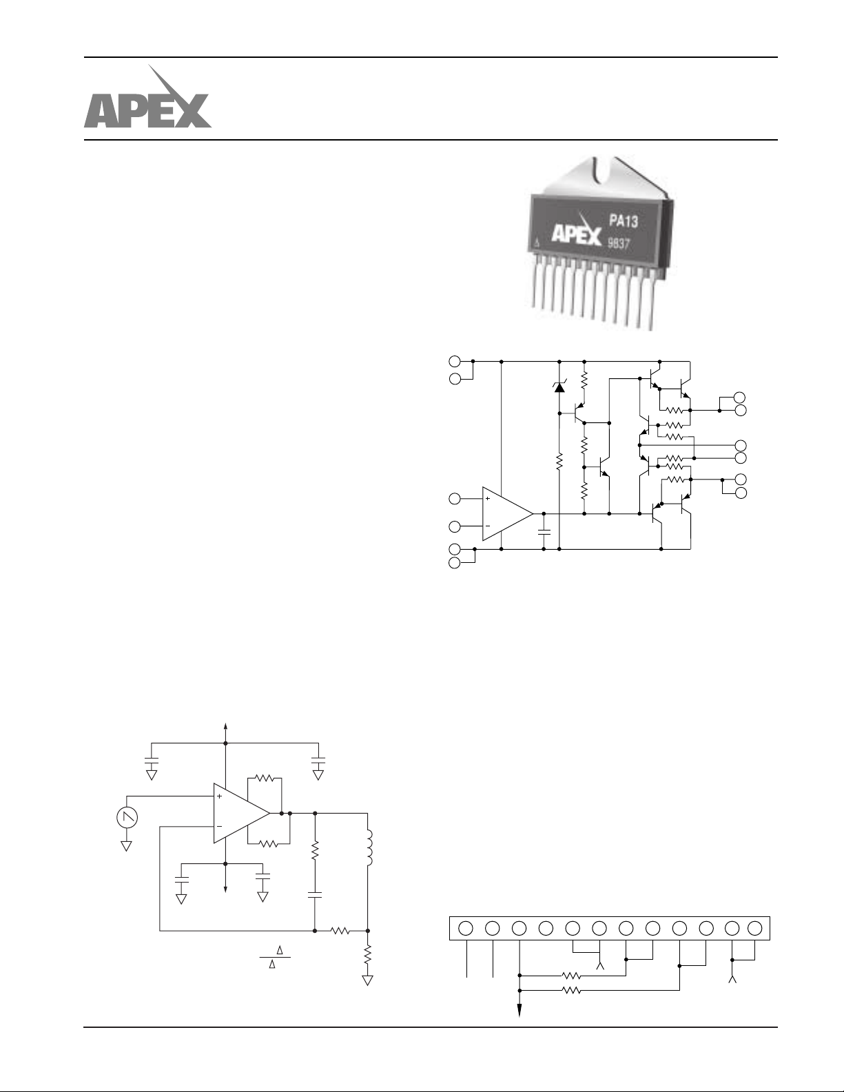
DESCRIPTION
The PA13 is a state of the art high voltage, very high output
current operational amplifier designed to drive resistive, inductive and capacitive loads. For optimum linearity, especially
at low levels, the output stage is biased for class A/B operation
using a thermistor compensated base-emitter voltage multiplier circuit. The safe operating area (SOA) can be observed
for all operating conditions by selection of user programmable current limiting resistors. For continuous operation
under load, a heatsink of proper rating is recommended.
This hybrid integrated circuit utilizes thick film (cermet)
resistors, ceramic capacitors and semiconductor chips to
maximize reliability, minimize size and give top performance.
Ultrasonically bonded aluminum wires provide reliable interconnections at all operating temperatures. The 12-pin power
SIP package is electrically isolated.
TYPICAL APPLICATION
+73V
HTTP://WWW.APEXMICROTECH.COM (800) 546-APEX (800) 546-2739
EQUIVALENT SCHEMATIC
12
Q3
Q5
Q2A
Q6A
Q2B
Q6B
10
9
3
4
7
8
11
2
A1
1
5
6
D1
Q1
Q4
C1
POWER RATING
Not all vendors use the same method to rate the power
handling capability of a Power Op Amp. APEX rates the
internal dissipation, which is consistent with rating methods
used by transistor manufacturers and gives conservative
results. Rating delivered power is highly application dependent and therefore can be misleading. For example, the 135W
internal dissipation rating of the PA13 could be expressed as
an output rating of 260W for audio (sine wave) or as 440W if
using a single ended DC load. Please note that all vendors rate
maximum power using an infinite heatsink.
47µF.1µF
11,12
2
2.5V
P-P
YOKE DRIVER:
HIGH CURRENT ASYMMETRICAL SUPPLY
APEX MICROTECHNOLOGY CORPORATION • TELEPHONE (520) 690-8600 • FAX (520) 888-3329 • ORDERS (520) 690-8601 • EMAIL prodlit@apexmicrotech.com
1
5,6
47µF
–22V
9,10
PA13
7,8
–V =
R
CL+
.2
R
.2
L * 1
Ω
CL–
Ω
t
3
.1µF
R
D
2K
C
F
50pF
R
1K
7.8mH
Ω
4
5Ap-p
F
R
S
Ω
.5
THERMAL STABILITY
APEX has eliminated the tendency of class A/B output
stages toward thermal runaway and thus has vastly increased
amplifier reliability. This feature, not found in most other Power
Op Amps, was pioneered by APEX in 1981 using thermistors
which assure a negative temperature coefficient in the quiescent current. The reliability benefits of this added circuitry far
outweigh the slight increase in component count.
EXTERNAL CONNECTIONS Package: SIP03
1234567891011 12
F.O.
–R
–IN +IN
OUTPUT
+R
–V
S
CL
CL
–C
L
+C
L
+V
S
PA13
ABSOLUTE MAXIMUM RATINGS
SPECIFICATIONS
ABSOLUTE MAXIMUM RATINGS
SUPPLY VOLTAGE, +Vs to –Vs 100V
OUTPUT CURRENT, within SOA 15A
POWER DISSIPATION, internal 135W
INPUT VOLTAGE, differential ±VS –3V
PA13/PA13A
INPUT VOLTAGE, common mode ±V
TEMPERATURE, pin solder -10s 300°C
TEMPERATURE, junction
1
S
175°C
TEMPERATURE RANGE, storage –65 to +150°C
OPERATING TEMPERATURE RANGE, case –55 to +125°C
SPECIFICATIONS
PARAMETER TEST CONDITIONS
2, 5
PA13 PA13A
MIN TYP MAX MIN TYP MAX UNITS
INPUT
OFFSET VOLTAGE, initial TC = 25°C ±2 ±6 ±1 ±3mV
OFFSET VOLTAGE, vs. temperature Full temperature range ±10 ±65 * ±40 µV/°C
OFFSET VOLTAGE, vs. supply TC = 25°C ±30 ±200 * * µV/V
OFFSET VOLTAGE, vs. power TC = 25°C ±20 * µV/W
BIAS CURRENT, initial TC = 25°C ±12 ±30 ±10 ±20 nA
BIAS CURRENT, vs. temperature Full temperature range ±50 ±500 * * pA/°C
BIAS CURRENT, vs. supply TC = 25°C ±10 * pA/V
OFFSET CURRENT, initial TC = 25°C ±12 ±30 ±5 ±10 nA
OFFSET CURRENT, vs. temperature Full temperature range ±50 * pA/°C
INPUT IMPEDANCE, DC TC = 25°C 200 * MΩ
INPUT CAPACITANCE TC = 25°C3*pF
COMMON MODE VOLTAGE RANGE3Full temperature range ±VS –5 ±VS –3** V
COMMON MODE REJECTION, DC Full temp. range, VCM = ±VS –6V 74 100 * * dB
GAIN
OPEN LOOP GAIN at 10Hz TC = 25°C, 1KΩ load 110 * dB
OPEN LOOP GAIN at 10Hz Full temp. range, 8Ω load 96 108 * * dB
GAIN BANDWIDTH PRODUCT @ 1MHz
TC = 25°C, 8Ω load 4 * MHz
POWER BANDWIDTH TC = 25°C, 8Ω load 13 20 * * kHz
PHASE MARGIN Full temp. range, 8Ω load 20 * °
OUTPUT
VOLTAGE SWING
VOLTAGE SWING
VOLTAGE SWING
3
3
3
T
= 25°C,
PA13
C
TC = 25°C, IO = 5A ±VS –5* V
= 10A, PA13A = 15A
±VS –6* V
Full temp. range, IO = 80mA ±VS–5* V
CURRENT, peak TC = 25°C1015A
SETTLING TIME to .1% TC = 25°C, 2V step 2 * µs
SLEW RATE TC = 25°C 2.5 4 * * V/µs
CAPACITIVE LOAD Full temperature range, AV = 1 1.5 * nF
CAPACITIVE LOAD Full temperature range, AV > 10 SOA *
POWER SUPPLY
VOLTAGE Full temperature range ±10 ±40 ±45 * * * V
CURRENT, quiescent TC = 25°C2550**mA
THERMAL
RESISTANCE, AC, junction to case
4
TC = –55 to +125°C, F > 60Hz .6 .7 * * °C/W
RESISTANCE, DC, junction to case TC = –55 to +125°C .9 1.1 * * °C/W
RESISTANCE, DC, junction to air TC = –55 to +125°C30*°C/W
TEMPERATURE RANGE, case Meets full range specification –25 +85 * * °C
NOTES: * The specification of PA13A is identical to the specification for PA13 in the applicable column to the left
1. Long term operation at the maximum junction temperature will result in reduced product life. Derate internal power dissipation
to achieve high MTTF.
2. The power supply voltage for all tests is ±40, unless otherwise noted as a test condition.
3. +VS and –VS denote the positive and negative supply rail respectively. Total VS is measured from +VS to –VS.
4. Rating applies if the output current alternates between both output transistors at a rate faster than 60Hz.
5. Full temperature range specifications are guaranteed but not 100% tested.
CAUTION
APEX MICROTECHNOLOGY CORPORATION • 5980 NORTH SHANNON ROAD • TUCSON, ARIZONA 85741 • USA • APPLICATIONS HOTLINE: 1 (800) 546-2739
The exposed substrate contains beryllia (BeO). Do not crush, machine, or subject to temperatures in excess of 850°C to
avoid generating toxic fumes.

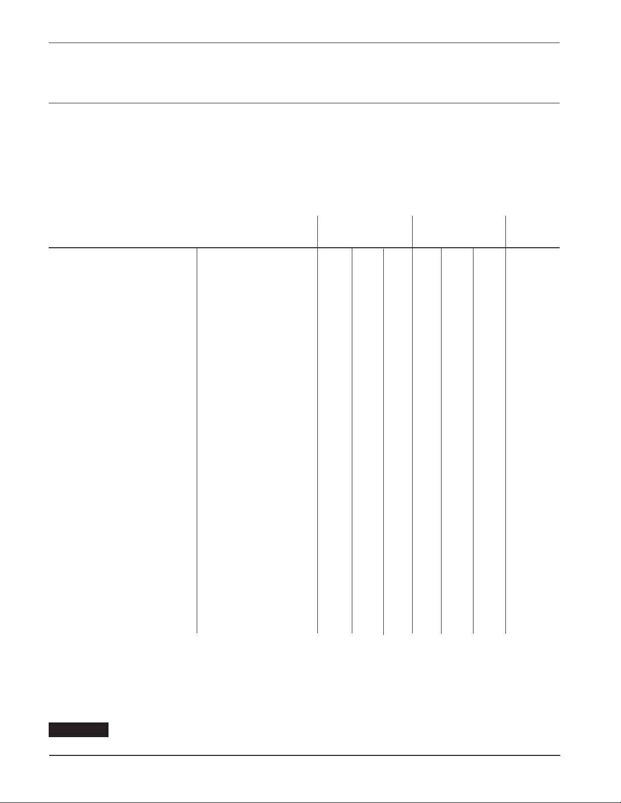
TYPICAL PERFORMANCE
GRAPHS
PA13
140
120
100
80
60
40
20
INTERNAL POWER DISSIPATION, P(W)
120
100
80
60
40
OPEN LOOP GAIN, A (dB)
–20
POWER DERATING
2.5
B
2.2
1.9
1.6
1.3
PA13
1.0
.7
0
0 20 40 60 80 100 120
CASE TEMPERATURE, T (°C)
140
.4
NORMALIZED BIAS CURRENT, I (X)
–50 0 100
SMALL SIGNAL RESPONSE
0
–30
–60
Φ
–90
–120
20
0
10 1K 10K .1M 1M 10 10K 1M
1 100 10M
PHASE, (°)
–150
–180
–210
FREQUENCY, F (Hz)
BIAS CURRENT
–25 25 50 75
CASE TEMPERATURE, T (°C)
PHASE RESPONSE
1 100 .1M 10M
FREQUENCY, F (Hz)
1K
17.5
CURRENT LIMIT
15.0
12.5
LIM
RCL = .06 ,RFO =
10.0
R
= .18 ,R
CL
7.5
5.0
V
= –24V
O
CURRENT LIMIT, I (A)
2.5
0
125
C
–50 –25 50 100
CASE TEMPERATURE, T (°C)
Ω
∞
= 0
Ω
FO
V
V
O
V
= 0
O
025 75
= 0
O
= 24V
C
125
POWER RESPONSE
100
68
PP
46
O
32
| +V
22
15
| +V
10
6.8
OUTPUT VOLTAGE, V (V )
4.6
10K 20K 50K .1M
| +V
| + |
S
| – | –V
| + |
S
| = 80V
S
–V
S
| = 30V
S
30K
FREQUENCY, F (Hz)
–V
| = 100V
S
70K
COMMON MODE REJECTION
120
100
80
60
40
20
0
1 10K
COMMON MODE REJECTION, CMR (dB)
HARMONIC DISTORTION
3
AV =10
1
VS = ±37V
RL = 4Ω
.3
.1
= 100mW
O
P
.03
DISTORTION, (%)
.01
.003
P
100 1K 3K .1M
300 10K 30K
1K 1M
FREQUENCY, F (Hz)
= 4W
O
P
= 120W
O
FREQUENCY, F (Hz)
.1M10 100
PULSE RESPONSE
8
6
O
4
VIN = ±5V, tr = 100ns
2
0
-2
-4
OUTPUT VOLTAGE, V (V)
-6
-8
2 4 6 8 10 12
0
TIME, t (µs)
QUIESCENT CURRENT
1.6
1.4
(X)
Q
1.2
1.0
.8
NORMALIZED, I
.6
.4
50 60 70 80 90
40 100
TOTAL SUPPLY VOLTAGE, V
= –25°C
T
C
= 25°C
T
C
= 85°C
T
C
T
C
= 125°C
S
(V)
100
INPUT NOISE
÷
70
N
50
40
30
20
10
INPUT NOISE VOLTAGE, V (nV/ Hz)
10 100 10K .1M
1K
FREQUENCY, F (Hz)
OUTPUT VOLTAGE SWING
6
5
–V
4
0
3
+V
0
2
1
VOLTAGE DROP FROM SUPPLY (V)
0
3691215
OUTPUT CURRENT, I
(A)
O
APEX MICROTECHNOLOGY CORPORATION • TELEPHONE (520) 690-8600 • FAX (520) 888-3329 • ORDERS (520) 690-8601 • EMAIL prodlit@apexmicrotech.com

PA13
OPERATING
CONSIDERATIONS
GENERAL
Please read Application Note 1 "General Operating Considerations" which covers stability, supplies, heat sinking, mounting,
current limit, SOA interpretation, and specification interpretation.
Visit www.apexmicrotech.com for design tools that help automate
tasks such as calculations for stability, internal power dissipation,
current limit; heat sink selection; Apex’s complete Application
Notes library; Technical Seminar Workbook; and Evaluation Kits.
±V
S
45V .43A 3.0A
40V .65A 3.4A
35V 1.0A 3.9A
30V 1.7A 4.5A
25V 2.7A 5.4A
SHORT TO ±V
C, L, OR EMF LOAD COMMON
S
SHORT TO
20V 3.4A 6.7A
SAFE OPERATING AREA (SOA)
The output stage of most power amplifiers has three distinct
limitations:
15V 4.5A 9.0A
These simplified limits may be exceeded with further analysis using the operating conditions for a specific application.
1. The current handling capability of the transistor geometry and
the wire bonds.
2. The second breakdown effect which occurs whenever the
simultaneous collector current and collector-emitter voltage
exceeds specified limits.
3. The junction temperature of the output transistors.
15
10
8
6
4
3
THERMAL
Tc=25°C
Tc=85°C
SECOND BREAKDOWN
2
t=1ms
t=1ms
steady state
t=0.5ms
1.5
1
.8
.6
.4
10 15 20 25 30 35 40 50 60 70 80 90
OUTPUT CURRENT FROM +V OR –V (A)
SUPPLY TO OUTPUT DIFFERENTIAL VOLTAGE V –V (V)
The SOA curves combine the effect of all limits for this Power Op
Amp. For a given application, the direction and magnitude of the
output current should be calculated or measured and checked
against the SOA curves. This is simple for resistive loads but more
complex for reactive and EMF generating loads. However, the
following guidelines may save extensive analytical efforts.
1. Capacitive and dynamic* inductive loads up to the following
maximum are safe with the current limits set as specified.
CAPACITIVE LOAD INDUCTIVE LOAD
±V
S
= 5A I
LIM
= 10A I
LIM
= 5A I
LIM
LIM
= 10A
I
50V 200µF 125µF 5mH 2.0mH
40V 500µF 350µF 15mH 3.0mH
35V 2.0mF 850µF 50mH 5.0mH
30V 7.0mF 2.5mF 150mH 10mH
25V 25mF 10mF 500mH 20mH
20V 60mF 20mF 1,000mH 30mH
15V 150mF 60mF 2,500mH 50mH
*If the inductive load is driven near steady state conditions, allowing the output
voltage to drop more than 12.5V below the supply rail with I
the supply rail with I
must be capacitively coupled or the current limit must be lowered to meet SOA
criteria.
= 5A while the amplifier is current limiting, the inductor
LIM
= 10A or 27V below
LIM
2. The amplifier can handle any EMF generating or reactive load
and short circuits to the supply rail or common if the current
limits are set as follows at T
This data sheet has been carefully checked and is believed to be reliable, however, no responsibility is assumed for possible inaccuracies or omissions. All specifications are subject to change without notice.
APEX MICROTECHNOLOGY CORPORATION • 5980 NORTH SHANNON ROAD • TUCSON, ARIZONA 85741 • USA • APPLICATIONS HOTLINE: 1 (800) 546-2739
= 25°C:
C
PA13U REV. F FEBRUARY 2001 © 2001 Apex Microtechnology Corp.
CURRENT LIMITING
Refer to Application Note 9, "Current Limiting", for details of both
fixed and foldover current limit operation. Visit the Apex web site
at www.apexmicrotech.com for a copy of Power_design.exe which
plots current limits vs. steady state SOA. Beware that current limit
should be thought of as a +/–20% function initially and varies about
2:1 over the range of –55°C to 125°C.
For fixed current limit, leave pin 4 open and use equations 1 and 2.
= 0.65/L
R
CL
= 0.65/R
I
CL
CL
CL
Where:
is the current limit in amperes.
I
CL
is the current limit resistor in ohms.
R
CL
For certain applications, foldover current limit adds a slope to
the current limit which allows more power to be delivered to the
load without violating the SOA. For maximum foldover slope,
ground pin 4 and use equations 3 and 4.
0.65 + (Vo * 0.014)
= (3)
I
CL
R
CL
0.65 + (Vo * 0.014)
= (4)
R
CL
I
CL
Where:
Vo is the output voltage in volts.
Most designers start with either equation 1 to set R
desired current at 0v out, or with equation 4 to set R
maximum output voltage. Equation 3 should then be used to plot
the resulting foldover limits on the SOA graph. If equation 3 results
in a negative current limit, foldover slope must be reduced. This
can happen when the output voltage is the opposite polarity of the
supply conducting the current.
In applications where a reduced foldover slope is desired, this
can be achieved by adding a resistor (R
) between pin 4 and
FO
ground. Use equations 4 and 5 with this new resistor in the circuit.
0.65 + Vo * 0.14
I
10.14 + R
= (5)
CL
R
CL
FO
0.65 + Vo * 0.14
R
Where:
is in K ohms.
R
FO
= (6)
10.14 + R
CL
I
CL
FO
for the
CL
CL
(1)
(2)
at the
 Loading...