

POWER OPERATIONAL AMPLIFIERS
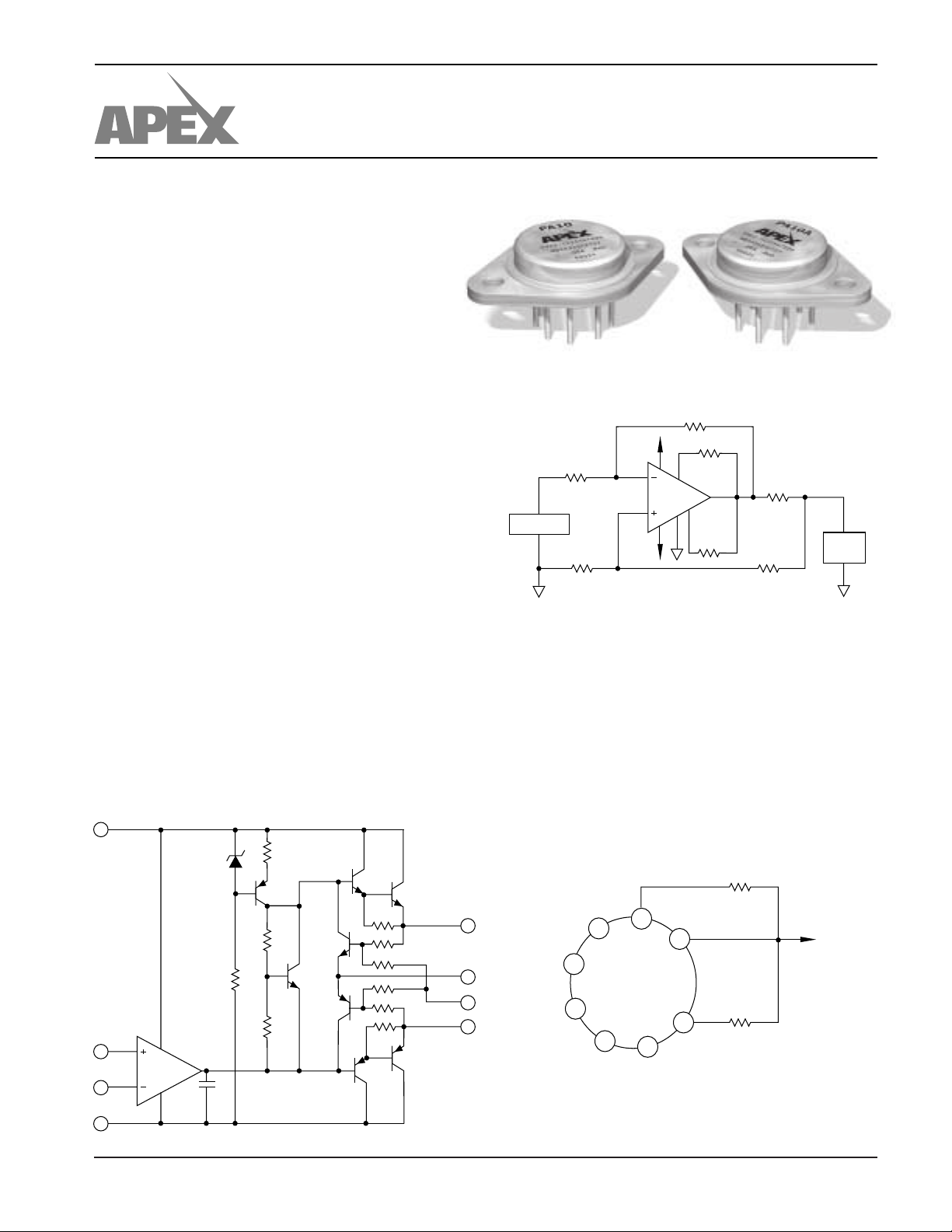
PA10 • PA10A
MICROTECHNOLOGY
FEATURES
• GAIN BANDWIDTH PRODUCT — 4MHz
• TEMPERATURE RANGE — –55 to +125°C (PA10A)
• EXCELLENT LINEARITY — Class A/B Output
• WIDE SUPPLY RANGE — ±10V to ±50V
• HIGH OUTPUT CURRENT — ±5A Peak
APPLICATIONS
• MOTOR, VALVE AND ACTUATOR CONTROL
• MAGNETIC DEFLECTION CIRCUITS UP TO 4A
• POWER TRANSDUCERS UP TO 100kHz
• TEMPERATURE CONTROL UP TO 180W
• PROGRAMMABLE POWER SUPPLIES UP TO 90V
• AUDIO AMPLIFIERS UP TO 60W RMS
DESCRIPTION
The PA10 and PA10A are high voltage, high output current
operational amplifiers designed to drive resistive, inductive and
capacitive loads. For optimum linearity, the output stage is
biased for class A/B operation. The safe operating area (SOA)
can be observed for all operating conditions by selection of user
programmable current limiting resistors. Both amplifiers are
internally compensated for all gain settings. For continuous
operation under load, a heatsink of proper rating is recommended.
This hybrid integrated circuit utilizes thick film (cermet)
resistors, ceramic capacitors and semiconductor chips to maximize reliability, minimize size and give top performance. Ultrasonically bonded aluminum wires provide reliable interconnections at all operating temperatures. The 8-pin TO-3 package is
hermetically sealed and electrically isolated. The use of compressible isolation washers voids the warranty.
EQUIVALENT SCHEMATIC
3
HTTP://WWW.APEXMICROTECH.COM (800) 546-APEX (800) 546-2739
TYPICAL APPLICATION
R2A
+42V
PA10
.82Ω
.82Ω
R2B
R
S
LOAD
0-24 Ω
R1A
CONTROL
R1B
–42V
FIGURE 1. VOLTAGE-TO-CURRENT CONVERSION
DC and low distortion AC current waveforms are delivered
to a grounded load by using matched resistors (A and B
sections) and taking advantage of the high common mode
rejection of the PA10.
Foldover current limit is used to modify current limits based
on output voltage. When load resistance drops to 0, the current
is limited based on output voltage. When load resistance
drops to 0, the current limit is 0.79A resulting in an internal
dissipation of 33.3 W. When output voltage increases to 36V,
the current limit is 1.69A. Refer to Application Note 9 on
foldover limiting for details.
D1
Q3
Q5
Q2A
Q6A
Q2B
Q6B
Q1
Q4
4
A1
5
6
APEX MICROTECHNOLOGY CORPORATION • TELEPHONE (520) 690-8600 • FAX (520) 888-3329 • ORDERS (520) 690-8601 • EMAIL prodlit@apexmicrotech.com
C1
EXTERNAL CONNECTIONS
+V
+IN
–IN
S
4
5
–V
2
1
7
8
3
TOP VIEW
6
S
FO
R
CL+
2
OUT
1
8
CL–
7
CL+
OUTPUT
R
CL–
PA10 • PA10A
ABSOLUTE MAXIMUM RATINGS
SPECIFICATIONS
ABSOLUTE MAXIMUM RATINGS
SUPPLY VOLTAGE, +VS to –V
OUTPUT CURRENT, within SOA 5A
S
100V
POWER DISSIPATION, internal 67W
INPUT VOLTAGE, differential ±VS –3V
INPUT VOLTAGE, common mode ±V
TEMPERATURE, pin solder - 10s 300°C
TEMPERATURE, junction
1
S
200°C
TEMPERATURE RANGE, storage –65 to +150°C
OPERATING TEMPERATURE RANGE, case –55 to +125°C
SPECIFICATIONS
PARAMETER TEST CONDITIONS
PA10
2, 5
MIN TYP MAX MIN TYP MAX UNITS
PA10A
INPUT
OFFSET VOLTAGE, initial TC = 25°C ±2 ±6 ±1 ±3mV
OFFSET VOLTAGE, vs. temperature Full temperature range ±10 ±65 * ±40 µV/°C
OFFSET VOLTAGE, vs. supply TC = 25°C ±30 ±200 * * µV/V
OFFSET VOLTAGE, vs. power TC = 25°C ±20 * µVW
BIAS CURRENT, initial TC = 25°C 1230 1020nA
BIAS CURRENT, vs. temperature Full temperature range ±50 ±500 * * pA/°C
BIAS CURRENT, vs. supply TC = 25°C.±10 * pA/V
OFFSET CURRENT, initial TC = 25°C ±12 ±30 ±5 ±10 nA
OFFSET CURRENT, vs. temperature Full temperature range ±50 * pA/°C
INPUT IMPEDANCE, DC TC = 25°C 200 * MΩ
INPUT CAPACITANCE TC = 25°C3*pF
COMMON MODE VOLTAGE RANGE3Full temperature range ±VS–5 ±VS–3** V
COMMON MODE REJECTION, DC
3
Full temp. range, VCM = ±VS –6V 74 100 * * dB
GAIN
OPEN LOOP GAIN at 10Hz TC = 25°C, 1KΩ load 110 * dB
OPEN LOOP GAIN at 10Hz Full temp. range, 15Ω load 96 108 * * dB
GAIN BANDWIDTH PRODUCT @ 1MHz TC = 25°C, 15Ω load 4 * MHz
POWER BANDWIDTH TC = 25°C, 15Ω load 10 15 * * kHz
PHASE MARGIN Full temp. range, 15Ω load 20 * °
OUTPUT
VOLTAGE SWING
VOLTAGE SWING
VOLTAGE SWING
3
3
3
TC = 25°C, IO = 5A ±VS–8 ±VS–5 ±VS–6* V
Full temp. range, IO = 2A ±VS–6* V
Full temp. range, IO = 80mA ±VS–5* V
CURRENT, peak TC = 25°C5*A
SETTLING TIME to .1% TC = 25°C, 2V step 2 * µs
SLEW RATE TC = 25°C23**V/µs
CAPACITIVE LOAD Full temperature range, AV = 1 .68 * nF
CAPACITIVE LOAD Full temperature range, AV = 2.5 10 * nF
CAPACITIVE LOAD Full temperature range, AV > 10 SOA * nF
POWER SUPPLY
VOLTAGE Full temperature range ±10 ±40 ±45 * * ±50 V
CURRENT, quiescent TC = 25°C 8 15 30 * * * mA
THERMAL
RESISTANCE, AC, junction to case
4
TC = –55 to +125°C, F > 60Hz 1.9 2.1 * * °C/W
RESISTANCE, DC, junction to case TC = –55 to +125°C 2.4 2.6 * * °C/W
RESISTANCE, junction to air TC = –55 to +125°C30*°C/W
TEMPERATURE RANGE, case Meets full range specifications –25 +85 –55 +125 °C
NOTES: * The specification of PA10A is identical to the specification for PA10 in applicable column to the left.
1. Long term operation at the maximum junction temperature will result in reduced product life. Derate internal power dissipation
to achieve high MTTF.
2. The power supply voltage for all tests is ±40, unless otherwise noted as a test condition.
3. +VS and –VS denote the positive and negative supply rail respectively. Total VS is measured from +VS to –VS.
4. Rating applies if the output current alternates between both output transistors at a rate faster than 60Hz.
5. Full temperature range specifications are guaranteed but not tested.
CAUTION
APEX MICROTECHNOLOGY CORPORATION • 5980 NORTH SHANNON ROAD • TUCSON, ARIZONA 85741 • USA • APPLICATIONS HOTLINE: 1 (800) 546-2739
The internal substrate contains beryllia (BeO). Do not break the seal. If accidentally broken, do not crush, machine, or
subject to temperatures in excess of 850°C to avoid generating toxic fumes.

TYPICAL PERFORMANCE
GRAPHS
PA10 • PA10A
70
60
50
POWER DERATING
T = T
C
40
30
PA10 PA10A
20
10
0
INTERNAL POWER DISSIPATION, P(W)
120
T = T
A
0 20 40 60 80 100 120
TEMPERATURE, T (°C)
SMALL SIGNAL RESPONSE
100
80
60
40
20
OPEN LOOP GAIN, A (dB)
0
–20
1 100 10M
10 1K 10K .1M 1M
FREQUENCY, F (Hz)
140
2.5
B
BIAS CURRENT
2.2
1.9
1.6
1.3
1.0
.7
.4
NORMALIZED BIAS CURRENT, I (X)
–25 25 50 75
–50 0 100
CASE TEMPERATURE, T (°C)
PHASE RESPONSE
0
–30
–60
–90
–120
PHASE, (°)ϕ
–150
–180
–210
0 100 .1M 10M
10 10K 1M
1K
FREQUENCY, F (Hz)
3.5
CURRENT LIMIT
3.0
2.5
LIM
R = 0.3CLΩ
2.0
1.5
R = 0.6CLΩ
1.0
CURRENT LIMIT, I (A)
.5
0
125
C
–50 –25 50 100
025 75
CASE TEMPERATURE, T (°C)
C
125
POWER RESPONSE
100
68
PP
46
O
32
22
15
10
6.8
OUTPUT VOLTAGE, V (V )
4.6
|+V | + |–V | = 100V
SS
|+V | + |–V | = 80V
SS
|+V | + |–V | = 30V
SS
10K 20K 50K .1M
30K
70K
FREQUENCY, F (Hz)
COMMON MODE REJECTION
120
100
80
60
40
20
0
0 10K
COMMON MODE REJECTION, CMR (dB)
HARMONIC DISTORTION
3
AV =10
1
V = ±38V
S
R =8
L
1K 1M
FREQUENCY, F (Hz)
Ω
.1M10 100 0
.3
.1
O
P = 50mW
O
.03
DISTORTION (%)
.01
.003
100 1K 3K .1M
P = 2W
O
P = 60W
300 10K 30K
FREQUENCY, F (Hz)
PULSE RESPONSE
8
6
O
4
V = ±5V, t = 100ns
IN r
2
0
–2
–4
OUTPUT VOLTAGE, V (V)
–6
–8
2 4 6 8 10 12
TIME, t (µs)
QUIESCENT CURRENT
Q
1.6
1.4
T = -25
C
°C
1.2
°C
T = 25
1.0
.8
.6
.4
40 100
50 60 70 80 90
TOTAL SUPPLY VOLTAGE, V (V)
NORMALIZED QUIESCENT CURRENT, I (X)
C
T = 85°C
C
T = 125
C
°C
S
100
INPUT NOISE
√
70
N
50
40
30
20
10
INPUT NOISE VOLTAGE, V (nV/ Hz)
10 100 10K .1M
1K
FREQUENCY, F (Hz)
OUTPUT VOLTAGE SWING
6
5
4
O
–V
3
O
+V
2
1
VOLTAGE DROP FROM SUPPLY, (V)
15
023
OUTPUT CURRENT, I (A)
°C
T = 25
C
T = 25 to 85
C
°C
T = 25
C
T = 25 to 85°C
C
°C
4
O
APEX MICROTECHNOLOGY CORPORATION • TELEPHONE (520) 690-8600 • FAX (520) 888-3329 • ORDERS (520) 690-8601 • EMAIL prodlit@apexmicrotech.com

PA10 • PA10A
OPERATING
CONSIDERATIONS
GENERAL
Please read Application Note 1 "General Operating Considerations" which covers stability, supplies, heat sinking, mounting,
current limit, SOA interpretation, and specification interpretation.
Visit www.apexmicrotech.com for design tools that help automate
tasks such as calculations for stability, internal power dissipation,
current limit; heat sink selection; Apex’s complete Application
Notes library; Technical Seminar Workbook; and Evaluation Kits.
SAFE OPERATING AREA (SOA)
The output stage of most power amplifiers has three distinct
limitations:
1. The current handling capability of the transistor geometry and
the wire bonds.
2. The second breakdown effect which occurs whenever the
simultaneous collector current and collector-emitter voltage
exceeds specified limits.
3. The junction temperature of the output transistors.
5.0
4.0
(A)
S
3.0
2.0
OR – V
S
1.5
1.0
Tc = 85°C
.8
.6
steady state SECOND BREAKDOWN
Tc = 125°C
THERMAL
t = 5ms
t = 0.5ms
t = 1ms
±V
SHORT TO ±V
S
C, L, OR EMF LOAD COMMON
S
SHORT TO
50V .21A .61A
40V .3A .87A
35V .36A 1.0A
30V .46A 1.4A
25V .61A 1.7A
20V .87A 2.2A
15V 1.4A 2.9A
CURRENT LIMITING
Refer to Application Note 9, "Current Limiting", for details of both
fixed and foldover current limit operation. Visit the Apex web site
at www.apexmicrotech.com for a copy of the Power Design
spreadsheet (Excel) which plots current limits vs. steady state
SOA. Beware that current limit should be thought of as a +/–20%
function initially and varies about 2:1 over the range of –55°C to
125°C.
For fixed current limit, leave pin 7 open and use equations 1 and 2.
= 0.65/L
R
CL
= 0.65/R
I
CL
CL
CL
Where:
is the current limit in amperes.
I
CL
is the current limit resistor in ohms.
R
CL
For certain applications, foldover current limit adds a slope to
the current limit which allows more power to be delivered to the
load without violating the SOA. For maximum foldover slope,
ground pin 7 and use equations 3 and 4.
(1)
(2)
.4
.3
OUTPUT CURRENT FROM +V
.2
10 15 20 25 30 35 40 50 60 70 80 100
SUPPLY TO OUTPUT DIFFERENTIAL VOLTAGE VS – VO (V)
The SOA curves combine the effect of these limits. For a given
application, the direction and magnitude of the output current
should be calculated or measured and checked against the SOA
curves. This is simple for resistive loads but more complex for
reactive and EMF generating loads.
1. For DC outputs, especially those resulting from fault condi-
tions, check worst case stress levels against the new SOA
graph.
For sine wave outputs, use Power Design
1
to plot a load line.
Make sure the load line does not cross the 0.5ms limit and that
excursions beyond any other second breakdown line do not
exceed the time label, and have a duty cycle of no more than
10%.
For other waveform outputs, manual load line plotting is
recommended. Applications Note 22, SOA AND LOAD LINES,
will be helpful. A Spice type analysis can be very useful in that
a hardware setup often calls for instruments or amplifiers with
wide common mode rejection ranges.
2. The amplifier can handle any EMF generating or reactive load
and short circuits to the supply rail or shorts to common if the
current limits are set as follows at T
1
Note 1. Power Design is a self-extracting Excel spreadsheet
= 85°C:
C
available free from www.apexmicrotech.com
0.65 + (Vo * 0.014)
= (3)
I
CL
R
CL
0.65 + (Vo * 0.014)
RCL = (4)
I
CL
Where:
Vo is the output voltage in volts.
Most designers start with either equation 1 to set R
desired current at 0v out, or with equation 4 to set R
maximum output voltage. Equation 3 should then be used to plot
for the
CL
CL
at the
the resulting foldover limits on the SOA graph. If equation 3 results
in a negative current limit, foldover slope must be reduced. This
can happen when the output voltage is the opposite polarity of the
supply conducting the current.
In applications where a reduced foldover slope is desired, this
can be achieved by adding a resistor (R
) between pin 7 and
FO
ground. Use equations 4 and 5 with this new resistor in the circuit.
0.65 + Vo
I
= (5)
CL
*
10.14 + R
R
CL
0.14
FO
0.65 + Vo * 0.14
10.14 + R
R
= (6)
CL
I
CL
FO
Where:
is in K ohms.
R
FO
This data sheet has been carefully checked and is believed to be reliable, however, no responsibility is assumed for possible inaccuracies or omissions. All specifications are subject to change without notice.
APEX MICROTECHNOLOGY CORPORATION • 5980 NORTH SHANNON ROAD • TUCSON, ARIZONA 85741 • USA • APPLICATIONS HOTLINE: 1 (800) 546-2739
PA10U REV. M FEBRURAY 2001 © 2001 Apex Microtechnology Corp.
 Loading...