

R
C
TOP VIEW
1
2
3
4
5
6
7
8
C
C
–V
S
+IN
–IN
+V
S
OUT
BAL
C
C
R
C
RS = (| +VS | + | –VS |) RT/1.6
NOTE: Input offset voltage trim optional. R
T
= 10K MAXΩ
R
T
R
S
PHASE COMPENSATION
C
C
100pF
15pF
5pF
none
GAIN
1
10
100
1000
R
C
200
0
0
none
Ω
Ω
Ω
VIDEO POWER OPERATIONAL AMPLIFIERS
MICROTECHNOLOGY
HTTP://WWW.APEXMICROTECH.COM (800) 546-APEX (800) 546-2739
FEATURES
• POWER MOS TECHNOLOGY — 2A peak rating
• HIGH GAIN BANDWIDTH PRODUCT — 150MHz
• VERY FAST SLEW RATE — 400V/µs
• PROTECTED OUTPUT STAGE — Thermal shutoff
• EXCELLENT LINEARITY — Class A/B output
• WIDE SUPPLY RANGE — ±12V to ±40V
• LOW BIAS CURRENT, LOW NOISE — FET input
PA09 • PA09A
APPLICATIONS
• VIDEO DISTRIBUTION AND AND AMPLIFICATION
• HIGH SPEED DEFLECTION CIRCUITS
• POWER TRANSDUCERS TO 5MHz
• COAXIAL LINE DRIVERS
• POWER LED OR LASER DIODE EXCITATION
DESCRIPTION
The PA09 is a high voltage, high output current operational
amplifier optimized to drive a variety of loads from DC through
the video frequency range. Excellent input accuracy is
achieved with a dual monolithic FET input transistor which is
cascoded by two high voltage transistors to provide outstanding common mode characteristics. All internal current and
voltage levels are referenced to a zener diode biased on by
a current source. As a result, the PA09 exhibits superior DC
and AC stability over a wide supply and temperature range.
High speed and freedom from second breakdown is assured by a complementary Power MOS output stage. For
optimum linearity, especially at low levels, the Power MOS
transistors are biased in the class A/B mode. Thermal shutoff
provides full protection against overheating and limits the
heatsink requirements to dissipate the internal power losses
under normal operating conditions. A built-in current limit
protects the amplifier against overloading. Transient inductive load kickback protection is provided by two internal
clamping diodes. External phase compensation allows the
user maximum flexibility in obtaining the optimum slew rate
and gain bandwidth product at all gain settings. For continuous operation under load, a heatsink of proper rating is
recommended.
This hybrid integrated circuit utilizes thick film (cermet) resistors,
ceramic capacitors and silicon semiconductor chips to maximize
reliability, minimize size and give top performance. Ultrasonically
bonded aluminum wires provide reliable interconnections at all
operating temperatures. The 8-pin TO-3
package is hermetically
sealed and electrically
isolated. The use of
com-pressible thermal
washers and/or improper mounting torque
will void the product
warranty. Please see
“General Operating
Considerations”.
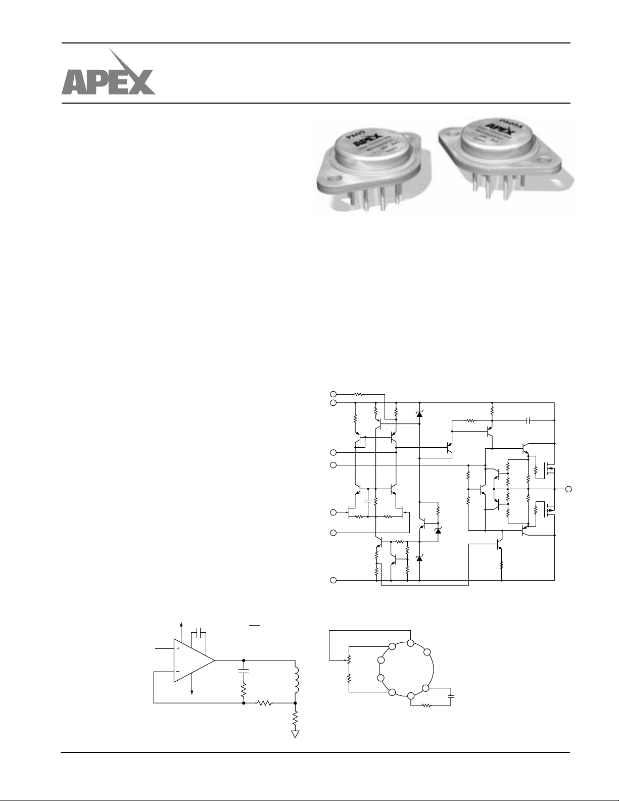
FIGURE 1. PA09 AS DEFLECTION AMPLIFIER
APEX MICROTECHNOLOGY CORPORATION • TELEPHONE (520) 690-8600 • FAX (520) 888-3329 • ORDERS (520) 690-8601 • EMAIL prodlit@apexmicrotech.com
V
I
+37V
3
4
PA09
5
C
7
6
2pF
C
–37V
8
1
470pF
C
R
12K
DEFLECTION AMPLIFIER (Figure 1)
The deflection amplifier circuit of Figure 1 achieves arbitrary
beam positioning for a fast heads-up display. Maximum transition times are 4µs while delivering 2A pk currents to the
13mH coil. The key to this circuit is the sense resistor (R
which converts yoke current to voltage for op amp feedback.
)
S
This negative feedback forces the coil current to stay exactly
proportional to the control voltage. The network consisting of
R
, RF and CF serves to shift from a current feedback via RS to
D
a direct voltage feedback at high frequencies. This removes
the extra phase shift caused by the inductor thus preventing
oscillation. See Application Note 5 for details of this and other
precision magnetic deflection circuits.
EQUIVALENT SCHEMATIC
2
3
7
8
5
4
6
Q12A
Q1
Q8
C2
Q5
Q15
Q18
Q2
Q9
Q12B
Q10
D1
Q3
Q4
Q13
Q11
Q14
D3
D2
C1
Q6
Q7
1
Q17
Q19
Q16
EXTERNAL CONNECTIONS
di
= 15A/µs
dt
i = Vi/R
S
R
100
F
Ω
L
Y
13µH
1
Ω
R
S
.5
Ω
F
D
PA09 • PA09A
ABSOLUTE MAXIMUM RATINGS
SPECIFICATIONS
ABSOLUTE MAXIMUM RATINGS
SUPPLY VOLTAGE, +VS to –V
OUTPUT CURRENT, within SOA 5A
POWER DISSIPATION, internal
S
1
80V
78W
INPUT VOLTAGE, differential 40V
INPUT VOLTAGE, common mode ±V
TEMPERATURE, pin solder - 10s 300°C
TEMPERATURE, junction
1
S
150°C
TEMPERATURE RANGE, storage –65 to +150°C
OPERATING TEMPERATURE RANGE, case –55 to +125°C
SPECIFICATIONS
PARAMETER TEST CONDITIONS
PA09
2
MIN TYP MAX MIN TYP MAX UNITS
PA09A
INPUT
OFFSET VOLTAGE, initial TC = 25°C.5± 3 ± .25 ± .5 mV
OFFSET VOLTAGE, vs. temperature TC = 25 to +85°C1030510µV/°C
OFFSET VOLTAGE, vs. supply TC = 25°C10*µV/V
OFFSET VOLTAGE, vs. power TC = 25 to +85°C20*µV/W
BIAS CURRENT, initial TC = 25°C 5 100 3 20 pA
BIAS CURRENT, vs. supply TC = 25°C .01 * pA/V
OFFSET CURRENT, initial TC = 25°C 2.5 50 1.5 10 pA
INPUT IMPEDANCE, DC TC = 25°C10
INPUT CAPACITANCE TC = 25°C6*pF
COMMON MODE VOLTAGE RANGE
3
TC = –25 to +85°C ± VS–10 ± VS–8 * * V
11
* Ω
COMMON MODE REJECTION, DC TC = –25 to +85°C, VCM = ± 20V 104 * dB
GAIN
OPEN LOOP GAIN at 10Hz TC = 25°C, RL = 1kΩ 90 * dB
OPEN LOOP GAIN at 10Hz TC = 25°C, RL = 15Ω 80 88 * * dB
GAIN BANDWIDTH PRODUCT at 1MHz TC = 25°C, RL = 15Ω, CC = 5pF 150 * MHz
POWER BANDWIDTH, gain of 100 comp TC = 25°C, RL = 15Ω, CC = 5pF 1.2 * MHz
POWER BANDWIDTH, unity gain comp TC = 25°C, RL = 15Ω, CC = 100pF .75 * MHz
OUTPUT
VOLTAGE SWING
3
TC = –25 to +85°C, IO = 2A ± VS –8 ± VS –7 * * V
CURRENT, PEAK TC = 25°C 4.5 * A
SETTLING TIME to .1% TC = 25°C, 2V step .3 * µs
SETTLING TIME to .01% TC = 25°C, 2V step 1.2 * µs
SLEW RATE, gain of 100 comp TC = 25°C, CC = 5pF 400 * V/µs
SLEW RATE, unity gain comp TC = 25°C, CC = 100pF 75 * V/µs
POWER SUPPLY
VOLTAGE TC = –25 to +85°C ± 12 ± 35 ± 40 * * * V
CURRENT, quiescent TC = 25°C7085**mA
THERMAL
RESISTANCE, AC junction to case
4
TC = –25 to +85°C, F > 60Hz 1.2 1.3 * * °C/W
RESISTANCE, DC junction to case TC = –25 to +85°C, F < 60Hz 1.6 1.8 * * °C/W
RESISTANCE, junction to air TC = –25 to +85°C30*°C/W
TEMPERATURE RANGE, case Meets full range specifications –25 25 + 85 * * * °C
NOTES: * The specification of PA09A is identical to the specification for PA09 in applicable column to the left.
1. Long term operation at the maximum junction temperature will result in reduced product life. Derate power dissipation to
achieve high MTTF.
2. The power supply voltage for all tests is ±35V unless otherwise specified as a test condition.
3. +VS and -VS denote the positive and negative supply rail respectively. Total VS is measured from +VS to –VS.
4. Rating applies if the output current alternates between both output transistors at a rate faster than 60Hz.
CAUTION
The internal substrate contains beryllia (BeO). Do not break the seal. If accidentally broken, do not crush, machine, or
subject to temperatures in excess of 850°C to avoid generating toxic fumes.
APEX MICROTECHNOLOGY CORPORATION • 5980 NORTH SHANNON ROAD • TUCSON, ARIZONA 85741 • USA • APPLICATIONS HOTLINE: 1 (800) 546-2739

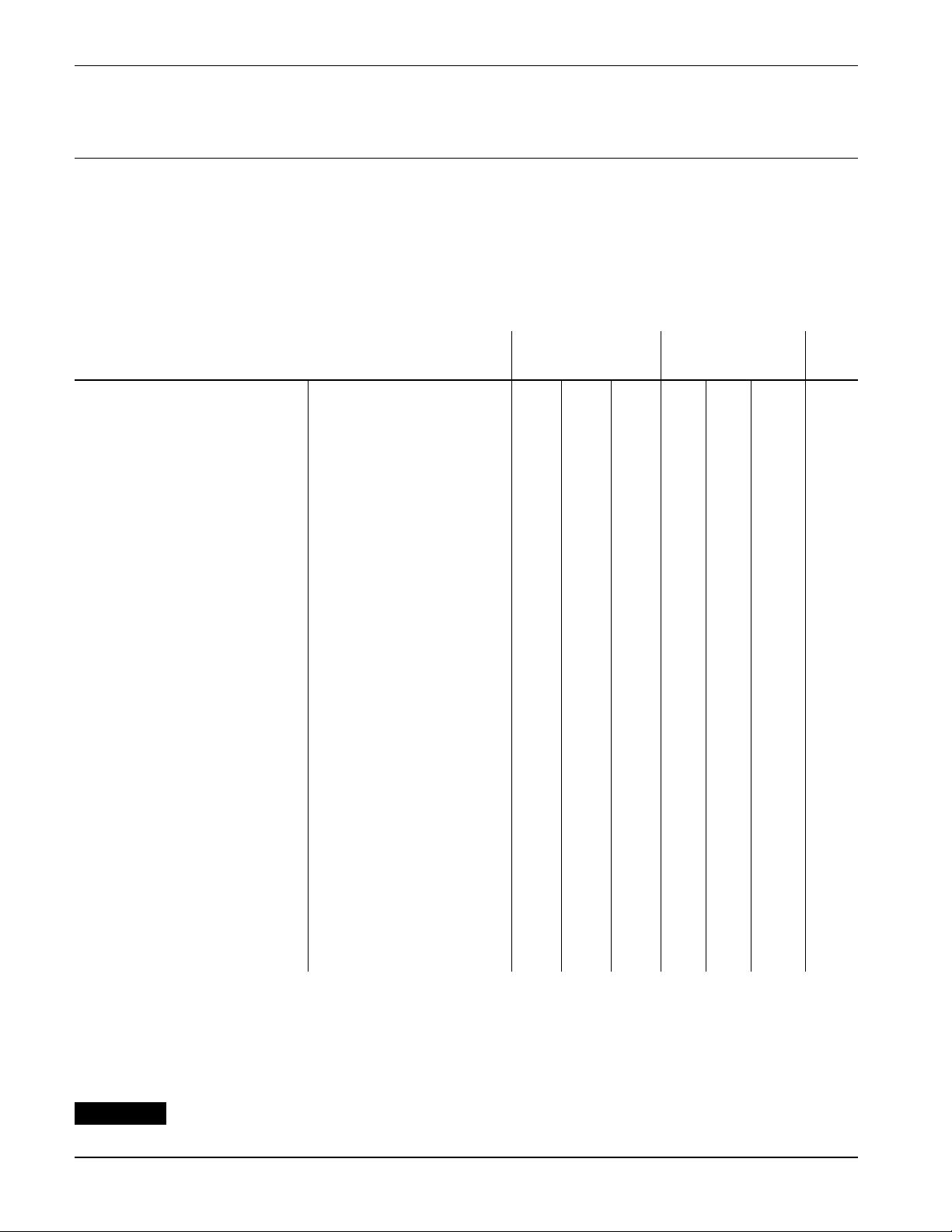
TYPICAL PERFORMANCE
, F(Hz)
GRAPHS
PA09 • PA09A
POWER DERATING
80
70
60
50
40
30
20
10
0
0 25 50 75 100 125
INTERNAL POWER DISSIPATION, P(W)
CASE TEMPERATURE, T
SMALL SIGNAL RESPONSE
100
80
60
40
20
0
OPEN LOOP GAIN, A (dB)
–20
600
500
400
300
200
150
SLEW RATE, (V/µs)
100
1K 100K
100 100M
SLEW RATE VS. COMP.
52030
COMPENSATION CAPACITOR, C
CC = 5pF
CC = 100pF
10K 1M 10M
FREQUENCY, F (Hz)
10 50 100
(°C)
C
CC = 15pF
C
COMMON MODE REJECTION
120
100
80
60
40
150
(pF)
9
8
7
(A)
LIM
6
5
4
3
CURRENT LIMIT, I
2
1
10
9
8
7
6
5
4
3
VOLTAGE DROP FROM SUPPLY (V)
30
20
(V)
O
10
0
–10
–20
OUTPUT VOLTAGE, V
–30
100
80
60
40
20
CURRENT LIMIT
–55 100
–25 25 50 75
JUNCTION TEMPERATURE, T
0
OUTPUT VOLTAGE SWING
0
OUTPUT CURRENT, IO (A)
2345
1
PULSE RESPONSE
Vin = ±2V, AV = 10, tr = 10ns
0.1.2.3.4
TIME, t (µs)
.5
.6 .7 .8
POWER SUPPLY REJECTION
(°C)
j
QUIESCENT CURRENT
(X)
1.6
Q
1.4
1.2
1.0
.8
125
.6
30 60 80
TOTAL SUPPLY VOLTAGE, V
NORMALIZED QUIESCENT CURRENT, I
70
50
PP
40
O
30
20
15
10
OUTPUT VOLTAGE, V (V )
| +VS | + | –VS | = 80V
7
100K 300K 3M 30M
30
√
20
(nV/ Hz)
N
15
10
7
5
3
INPUT NOISE VOLTAGE, V
10 100 10K 1M
COMMON MODE VOLTAGE
)
70
PP
(V
50
CM
40
30
20
15
10
40 50 70
POWER RESPONSE
C
C
C
= 15pF
C
= 100pF
1M
FREQUENCY, F (Hz)
INPUT NOISE
1K
FREQUENCY, F (Hz)
| +VS | + | –VS | = 80V
CC= 100pF
10M
100K
S
(V)
20
1K 10M
COMMON MODE REJECTION, CMR (dB)
10K 100K
FREQUENCY, F (Hz)
1M
100M
0
1K
POWER SUPPLY REJECTION, PSR (dB)
10K 100K 1M 100M
FREQUENCY, F(Hz)
10M
7
100K
COMMON MODE VOLTAGE, V
300K 1M 3M 10M 30M
FREQUENCY
APEX MICROTECHNOLOGY CORPORATION • TELEPHONE (520) 690-8600 • FAX (520) 888-3329 • ORDERS (520) 690-8601 • EMAIL prodlit@apexmicrotech.com

PA09 • P A09A
OPERATING
CONSIDERATIONS
GENERAL
Please read the “General Operating Considerations” section, which covers stability, supplies, heatsinking, mounting,
current limit, SOA interpretation, and specification interpretation. Additional information can be found in the application
notes. For information on the package outline, heatsinks, and
mounting hardware, consult the “Accessory and Package
Mechanical Data” section of the handbook.
SUPPLY VOLTAGE
The specified voltage (±VS) applies for a dual (±) supply
having equal voltages. A nonsymmetrical (ie. +70/–10V) or a
single supply (ie. 80V) may be used as long as the total voltage
between the +V
and –VS rails does not exceed the sum of the
S
voltages of the specified dual supply.
SAFE OPERATING AREA (SOA)
The MOSFET output stage of this power operational amplifier has two distinct limitations:
1. The current handling capability of the MOSFET geometry
and the wire bonds.
2. The junction temperature of the output MOSFETs.
SAFE OPERATING AREA CURVES
5.0
(A)
S
4.0
3.5
OR –V
S
3.0
2.5
2.0
steady state
TC = 25°C
t = 100ms
t = 300ms
tantalum capacitor of at least 47µF in parallel with a .47µF
ceramic capacitor directly connected from the power supply
pins to the ground plane.
OUTPUT LEADS
Keep the output leads as short as possible. In the video
frequency range, even a few inches of wire have significant
inductance, raising the interconnection impedance and limiting the output current slew rate. Furthermore, the skin effect
increases the resistance of heavy wires at high frequencies.
Multistrand Litz Wire is recommended to carry large video
currents with low losses.
GROUNDING
Single point grounding of the input resistors and the input
signal to a common ground plane will prevent undesired
current feedback, which can cause large errors and/or instabilities.
THERMAL SHUTDOWN PROTECTION
The thermal protection circuit shuts off the amplifier when
the substrate temperature exceeds approximately 150°C. This
allows heatsink selection to be based on normal operating
conditions while protecting the amplifier against excessive
junction temperature during temporary fault conditions.
Thermal protection is a fairly slow-acting circuit and therefore does not protect the amplifier against transient SOA
violations (areas outside of the T
designed to protect against short-term fault conditions that
result in high power dissipation within the amplifier, If the
conditions that cause thermal shutdown are not removed, the
amplifier will oscillate in and out of shutdown. This will result in
high peak power stresses, destroy signal integrity, and reduce
the reliability of the device.
= 25°C boundary). It is
C
1.5
20 40
25
INTERNAL VOLTAGE DROP SUPPLY TO OUTPUT VS –VO (V)
OUTPUT CURRENT FROM +V
15
30
35
50
60
70
80
The SOA curves combine the effect of these limits and allow
for internal thermal delays. For a given application, the direction and magnitude of the output current should be calculated
or measured and checked against the SOA curves. This is
simple for resistive loads but more complex for reactive and
EMF generating loads. The following guidelines may save
extensive analytical efforts:
1. Capacitive and inductive loads up to the following maxi-
mums are safe:
±V
S
40V .1µF 11mH
CAPACITIVE LOAD INDUCTIVE LOAD
30V 500µF 24mH
20V 2500µF 75mH
15V ∞ 100mH
2. Short circuits to ground are safe with dual supplies up to
±20V.
3. The output stage is protected against transient flyback.
However, for protection against sustained, high energy
flyback, external fast-recovery diodes should be used.
BYPASSING OF SUPPLIES
Each supply rail must be bypassed to common with a
STABILITY
Due to its large bandwidth the PA09 is more likely to oscillate
than lower bandwidth Power Operational Amplifiers. To prevent oscillations a reasonable phase margin must be maintained by:
1. Selection of the proper phase compensation capacitor and
resistor. Use the values given in the table under external
connections on the first page of this data sheet and interpolate if necessary. The phase margin can be increased by
using a larger capacitor and a smaller resistor than the slew
rate optimized values listed in the table.
2. Keeping the external sumpoint stray capacitance to ground
at a minimum and the sumpoint load resistance (input and
feedback resistors in parallel) below 500Ω. Larger sumpoint
load resistances can be used with increased phase compensation and/or bypassing of the feedback resistor.
3. Connect the case to a local AC ground potential.
CURRENT LIMIT
Internal current limiting is provided in the PA09. Note the
current limit curve given under typical performance graphs is
based on junction temperature. If the amplifier is operated at
cold junction temperatures, current limit could be as high as 8
amps. This is above the maximum allowed current on the SOA
curve of 5 amps. Systems using this part must be designed to
keep the maximum output current to less than 5 amps under
all conditions. The internal current limit only provides this
protection for junction temperatures of 80°C and above.
This data sheet has been carefully checked and is believed to be reliable, however, no responsibility is assumed for possible inaccuracies or omissions. All specifications are subject to change without notice.
PA09U REV. H FEBRUARY 1998 © 1998 Apex Microtechnology Corp.
 Loading...