

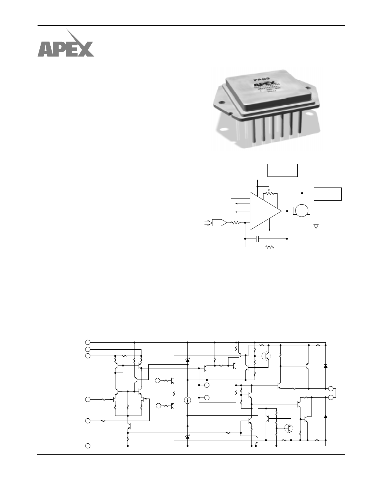
POSITION
FEEDBACK
OBJECT
TOOL
SHUT DOWN
+5V
+
+S
–S
–
–V
S
C
1
R2
R
BAL
+V
S
0/10V
R1
PA03
DESIRED
POSITION
DAC
POWER OPERATIONAL AMPLIFIERS
MICROTECHNOLOGY
HTTP://WWW.APEXMICROTECH.COM (800) 546-APEX (800) 546-2739
FEA TURES
• MO-127 COPPER POWER DIP™ PACKAGE
• HIGH INTERNAL POWER DISSIPATION
— 500 watts
• HIGH VOLTAGE OPERATION — ±75V
• VERY HIGH CURRENT — ±30 amps
• INTERNAL SOA PROTECTION
• OUTPUT SWINGS CLOSE TO SUPPLY RAILS
• EXTERNAL SHUTDOWN CONTROL
APPLICATIONS
• LINEAR AND ROTARY MOTOR DRIVES
• YOKE/MAGNETIC FIELD DEFLECTION
• PROGRAMMABLE POWER SUPPLIES to ±68V
• TRANSDUCER/AUDIO TO 1000W
DESCRIPTION
The super power PA03 advances the state of the art in both
brute force power and self protection against abnormal operating conditions. Its features start with a copper dip package
developed by Apex to extend power capabilities well beyond
those attainable with the familiar TO-3 package. The increased pin count of the new package provides additional
control features, while the superior thermal conductivity of
copper allows substantially higher power ratings.
The PA03 incorporates innovative current limiting circuits
limiting internal power dissipation to a curve approximating the
safe operating area of the power transistors. The internal
current limit of 35A is supplemented with thermal sensing
which reduces the current limit as the substrate temperature
rises. Furthermore, a subcircuit monitors actual junction temperatures and with a response time of less than ten milliseconds reduces the current limit further to keep the junction
temperature at 175°C.
The PA03 also features a laser trimmed high performance
FET input stage providing superior DC accuracies both initially
and over the full temperature range.
PA03 • P03A
TYPICAL APPLICATION
The PA03 output power stages contain fast reverse recov-
ery diodes for sustained high energy flyback protection.
This hybrid integrated circuit utilizes thick film resistors,
ceramic capacitors and silicon semiconductors to maximize
reliability, minimize size and give top performance. Ultrasonically bonded aluminum wires provide reliable interconnections at all operating temperatures. The MO-127 Copper,
12-pin Power Dip™ package (see Package Outlines), is
hermetically sealed and isolated from the internal circuits.
Insulating washers are not recommended.
IMPORTANT: Observe mounting precautions.
+V
8
BAL
11
BAL
12
Q5
Q31
Q20
B
Q3
Q18
4
+SHUT
DOWN
Q22
3
–SHUT
DOWN
Q2
Q17
–
1
+
2
–V
5
Q20
A
Q14
D1
Q12
9
COMP
10
D4
Q6
Q1
Q7
Q19
Q29
Q34
Q4
Q30
Q16
Q32
Q24
Q9
Q26
D2
+
7
6
–
D3
EQUIVALENT
SCHEMATIC
APEX MICROTECHNOLOGY CORPORATION • TELEPHONE (520) 690-8600 • FAX (520) 888-3329 • ORDERS (520) 690-8601 • EMAIL prodlit@apexmicrotech.com
OUT
PA03 • PA03A
ABSOLUTE MAXIMUM RATINGS
SPECIFICATIONS
ABSOLUTE MAXIMUM RATINGS
SUPPLY VOLTAGE, +VS to –V
OUTPUT CURRENT, within SOA Internally limited
S
POWER DISSIPATION, internal 500W
INPUT VOLTAGE, differential ±25V
INPUT VOLTAGE, common mode ±V
TEMPERATURE, pin solder-10s 300°C
TEMPERATURE, junction
1
TEMPERATURE RANGE, storage –65 to +150°C
OPERATING TEMP. RANGE, case –55 to +125°C
SHUTDOWN VOLTAGE, differential ±5V
SHUTDOWN VOLTAGE, common mode ±V
150V
S
175°C
S
–SHUT DN
+SHUT DN
–OUTPUT
SPECIFICATIONS
PARAMETER TEST CONDITIONS
–INPUT
+INPUT
–SUPPLY
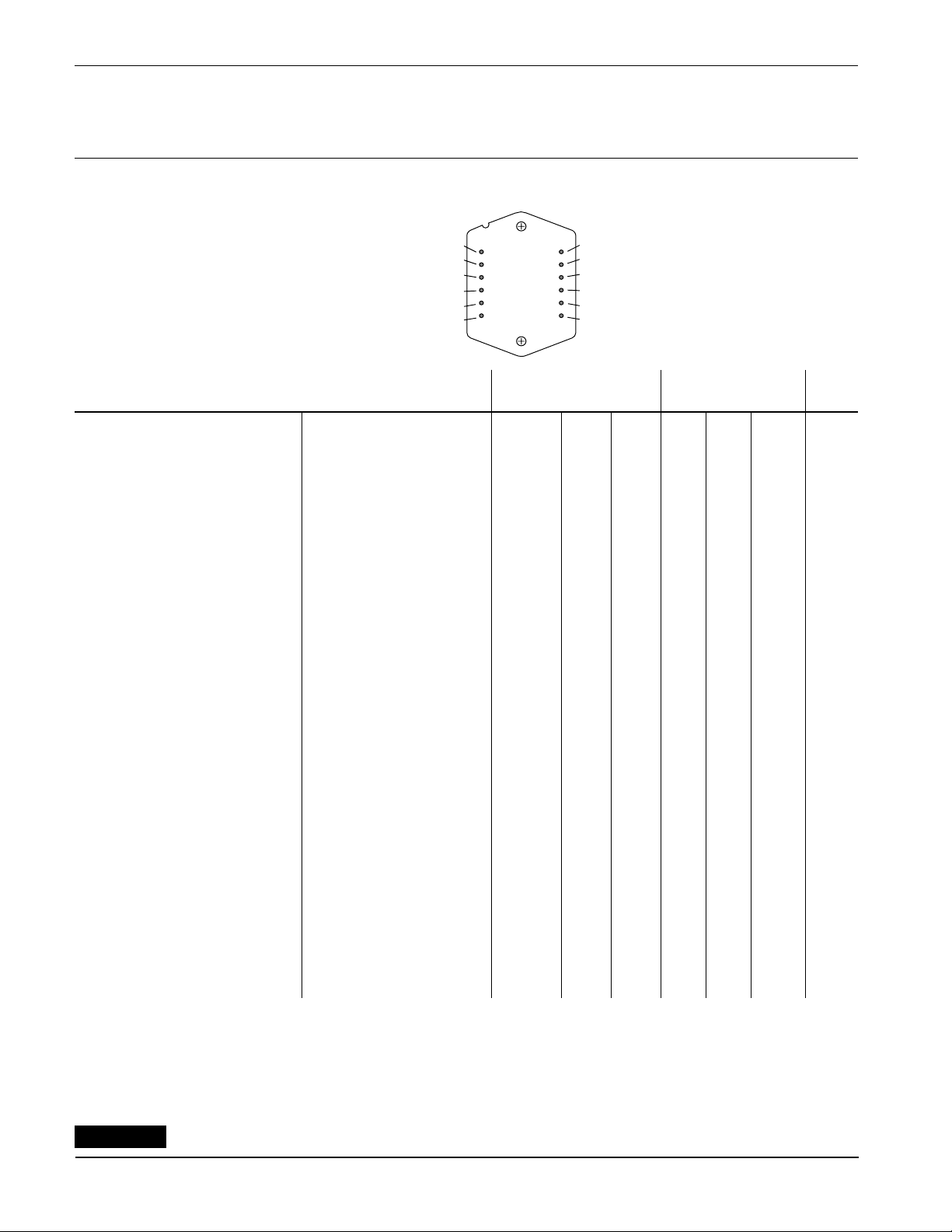
EXTERNAL CONNECTIONS
1
2
3
4
5
6
2
12
11
TOP
10
VIEW
†
MIN TYP MAX MIN TYP MAX UNITS
BALANCE CONTROL
BALANCE CONTROL
PHASE COMP.
9
PHASE COMP.
8
+SUPPLY
7
+OUTPUT
PA03
Pins 6 & 7 must be
connected together.
If unused, tie Pins
11 & 12 to +SUPPLY.
† IMPORTANT: OBSERVE
MOUNTING PRECAUTIONS.
REVERSE INSERTION
WILL DESTROY UNIT.
PA03A
INPUT
OFFSET VOLTAGE, initial TC = 25°C ± .5 ± 2 ± .25 ± .5 mV
OFFSET VOLTAGE, vs. temperature Full temperature range 10 30 5 10 µV/°C
OFFSET VOLTAGE, vs. supply TC = 25°C8*µV/V
OFFSET VOLTAGE, vs. power Full temperature range 20 10 µV/W
BIAS CURRENT, initial TC = 25°C550310pA
BIAS CURRENT, vs. supply TC = 25°C .01 * pA/V
OFFSET CURRENT, initial TC = 25°C 2.5 50 1.5 10 pA
INPUT IMPEDANCE, DC TC = 25°C10
11
* Ω
INPUT CAPACITANCE TC = 25°C6*pF
COMMON MODE VOLTAGE RANGE3Full temperature range ± VS –10V * V
COMMON MODE REJECTION, DC Full temp. range, VCM = ±20V 86 108 * * dB
SHUTDOWN CURRENT
4
Full temperature range 100 * µA
SHUTDOWN VOLTAGE Full temp. range, amp enabled .85 * V
SHUTDOWN VOLTAGE Full temp. range, amp disabled 3.5 * V
GAIN
OPEN LOOP GAIN at 10Hz Full temp. range, full load 92 102 * * dB
GAIN BANDWIDTH PRODUCT at 1MHz TC = 25°C, full load 1 * MHz
POWER BANDWIDTH TC = 25°C, IO = 15A, VO = 88V
PHASE MARGIN Full temp. range, CC = 1.8nF 65 * °
PP
30 * kHz
OUTPUT
VOLTAGE SWING
VOLTAGE SWING
VOLTAGE SWING
3
3
3
TC = 25°C, IO = 30A ± VS –7 6.2 * * V
Full temp. range, IO = 12A ± VS –5 4.2 * * V
Full temp. range, IO = 146mA ± VS –4 3.5 * * V
CURRENT, peak TC = 25°C30*A
SETTLING TIME to .1% TC = 25°C, 10V step 8 * µs
SLEW RATE TC = 25°C, CC - open 8 * V/µs
CAPACITIVE LOAD Full temp. range, AV = 1 2 * nF
SHUTDOWN DELAY TC = –25°C, disable 10 * µs
TC = –25°C, operate 20 * µs
POWER SUPPLY
VOLTAGE Full temperature range ± 15 ± 50 ± 75 * * * V
CURRENT, quiescent
6
TC = 25°C 125 300 * * mA
CURRENT, disable mode Full temperature range 25 40 * * mA
THERMAL
RESISTANCE, AC junction to case
5
Full temp. range, F>60Hz .22 .28 * * °C/W
RESISTANCE, DC junction to case Full temp. range, F<60Hz .25 .3 * * °C/W
RESISTANCE, junction to ambient Full temperature range 14 * °C/W
TEMPERATURE, junction Sustained operation 150 * °C
TEMPERATURE RANGE, case Meets full range specification – 25 85 * * °C
NOTES: * The specification of PA03A is identical to the specification for PA03 in applicable column to the left.
1. Long term operation at the maximum junction temperature will result in reduced product life. Derate power dissipation to
achieve high MTTF.
2. The power supply voltage for all specifications is the TYP rating unless noted as a test condition.
3. +VS and –VS denote the positive and negative supply rail respectively. Total VS is measured from +VS to –VS.
4. Rating applies if both shutdown inputs are least 1V inside supply rails. If one of the shutdown inputs is tied to a supply rail, the
current in that pin may increase to 2.4mA.
5. Rating applies if the output current alternates between both output transistors at a rate faster than 60Hz.
6. The PA03 must be used with a heatsink or the quiescent power may drive the unit into thermal shutdown.
CAUTION
APEX MICROTECHNOLOGY CORPORATION • 5980 NORTH SHANNON ROAD • TUCSON, ARIZONA 85741 • USA • APPLICATIONS HOTLINE: 1 (800) 546-2739
The internal substrate contains beryllia (BeO). Do not break the seal. If accidentally broken, do not crush, machine, or
subject to temperatures in excess of 850°C to avoid generating toxic fumes.
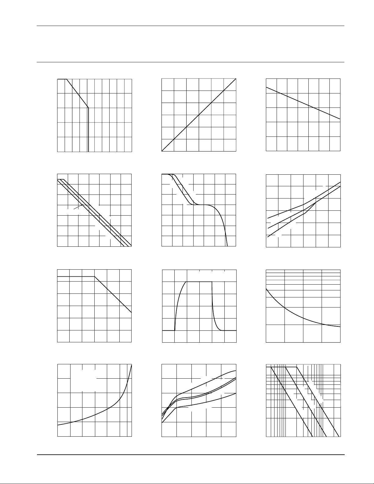
TYPICAL PERFORMANCE
GRAPHS
PA03 • PA03A
500
POWER DERATING
400
300
200
100
0
0
INTERNAL POWER DISSIPATION, P(W)
40 80 120 160 200
CASE TEMPERATURE, T (°C)
C
SMALL SIGNAL RESPONSE
120
100
80
C
C
60
CC = 470pF
40
20
OPEN LOOP GAIN, A (dB)
0
–20
1 100 10M
10 1K 10K .1M 1M
FREQUENCY, F (Hz)
COMMON MODE REJECTION
120
100
80
= OPEN
C
C
= 1800pF
BIAS CURRENT
B
256
64
16
4
1
.25
.06
NORMALIZED BIAS CURRENT, I (X)
5456585
–15 105
25
CASE TEMPERATURE, T (°C)
C
PHASE RESPONSE
0
–30
–60
Φ
–90
–120
PHASE, (°)
–150
–180
–210
1 100 .1M 10M
7.5
5.0
2.5
C
C
C
= OPEN
C
= 1800pF
10 10K 1M
1K
FREQUENCY, F (Hz)
PULSE RESPONSE
VIN = ±.5V, AV = 10
RL =.5Ω
50
CURRENT LIMIT
40
LIM
30
20
10
CURRENT LIMIT, I (A)
0
–50 –25 0
CASE TEMPERATURE, T (°C)
OUTPUT VOLTAGE SWING
7
25 75
50 100
C
6
5
= –55°C
C
T
4
= 25°C
C
T
3
= 125°C
C
T
2
1
VOLTAGE DROP FROM SUPPLY (V)
0 5 20 25
20
10
OUTPUT CURRENT, I
INPUT NOISE
O
√
(nV/ Hz)
10
N
125
3015
(A)
60
0
6
VOLTS
40
–2.5
4
20
0
1 10K
COMMON MODE REJECTION, CMR (dB)
1.0
0.3
FREQUENCY, F (Hz)
HARMONIC DISTORTION
VS = ±50V
A
P
R
0.1
1K 1M
= 10
V
= 200W
O
= 4 Ω
L
.1M10 100
.03
DISTORTION, (%)
.01
.003
30 100 300 1K 3K 10K 30K
FREQUENCY, F (Hz)
–5.0
–7.5
1.4
51015202530
0
TIME, t (µS)
QUIESCENT CURRENT
1.2
C
(X)
Q
1.0
.8
NORMALIZED, I
.6
.4
40
T
T
60 80 100 120 140
TOTAL SUPPLY VOLTAGE, V
= 125°C
= 85°C
C
C
T
= 25°C
= –25°C
C
T
2
INPUT NOISE VOLTAGE, V
10 100 10K .1M
1K
FREQUENCY, F (Hz)
150
)
100
PP
(V
O
POWER RESPONSE
50
40
C
C
C
C
= 1800pF
C
C
= OPEN
= 470pF
30
20
OUTPUT VOLTAGE, V
10
5K
3K
10K 50K 100K
(V)
S
FREQUENCY, F (Hz)
300K
APEX MICROTECHNOLOGY CORPORATION • TELEPHONE (520) 690-8600 • FAX (520) 888-3329 • ORDERS (520) 690-8601 • EMAIL prodlit@apexmicrotech.com
PA03 • PA03A
OPERATING
CONSIDERATIONS
GENERAL
Please read the “General Operating Considerations” section,
which covers stability, supplies, heatsinking, mounting, current
limit, SOA interpretation, and specification interpretation. Additional information can be found in the application notes. For
information on the package outline, heatsinks, and mounting
hardware, consult the “Accessory and Package Mechanical Data”
section of the handbook.
MOUNTING PRECAUTIONS
The PA03 copper base is very soft and easily bent. Do not put
any stress on the mounting ears of this package. This calls for
caution when pushing the amplifier into certain types of packaging
foam and particularly when inserting the device into a socket.
Insert the amplifier into the socket only by pushing on the perimeter
of the package lid. Pushing the unit into the socket by applying
pressure to the mounting tabs will bend the base due to the high
insertion force required. The base will then not contact the heatsink
evenly resulting in very poor heat transfer. To remove a unit from
a socket, pry the socket away from the heatsink so that the
heatsink will support the amplifier base evenly. Recommended
mounting torque is 8–10 in.-lbs. (.9–1.13 N•m).
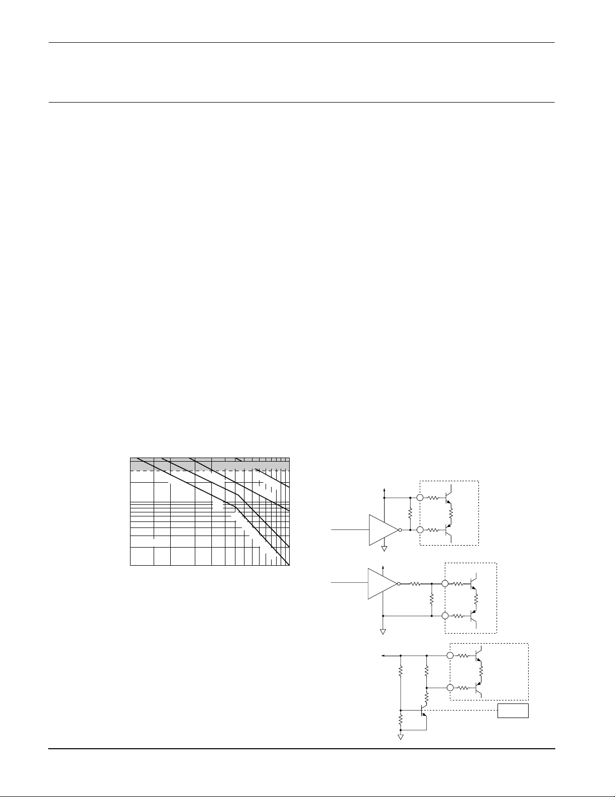
SAFE OPERATING AREA (SOA)
Due to the internal (non-adjustable) current limit of the PA03,
worst case power dissipation calculations must assume current
capability of 46 amps. Application specific circuits should be
checked against the SOA curve when relying upon current limit for
fault protectio
n.
SAFE OPERATING AREA CURVES
Second breakdown limitations do apply to the PA03 but are
less severe, since junction temperature limiting responds
within 10ms. Stress levels shown as being safe for more than
10ms duration
will merely
cause thermal
shutdown.
Under normal operating
conditions, activation of the
)
40
(A
S
30
OR –V
S
10
5
THERMAL
CURRENT LIMIT ZONE
100mS
dc
SECOND BREAKDOWN
1.0mS
10mS
thermal shutdown is a sign
that the internal junction
temperatures
have reached
approximately
TC = 25°C
1
10 20 50 100 150
SUPPLY TO OUTPUT DIFFERENTIAL VS –VO (V)
OUTPUT CURRENT FROM +V
175°C. Thermal shutdown is a short term safety feature. If the
conditions remain that cause thermal shutdown, the amplifier
will oscillate in and out of shutdown, creating peak high power
stresses, destroying useful signals, and reducing the reliability
of the device.
BALANCE CONTROL
The voltage offset of the PA03 may be externally adjusted to
zero. To implement this adjustment install a 100 to 200 ohm
potentiometer between pins 11 and 12 and connect the wiper arm
to the positive supply. Bypass pins 11 and 12 each with at least a
.01µF ceramic capacitor.
If the optional adjust provision is not used, connect both pins 11
and 12 to the positive supply.
OUTPUT STAGE SHUTDOWN
The entire power stage of the PA03 may be disabled using one
of the circuits shown in Figure 1. There are many applications for
this function. One is a load protection based on power delivered to
the load or thermal rise. Another one is conservation of power
when using batteries. The control voltage requirements accommodate a wide variety logic drivers.
1. CMOS operating at +5V can drive the control pins directly.
2. CMOS operating at greater than 5V supplies need a voltage
divider.
3. TTL logic needs a pull up resistor to +5V to provide a swing to
the fully disabled voltage (3.5V). When not using the shutdown
feature, connect both pins 3 and 4 to common.
PHASE COMPENSATION
At low gain settings an external compensation capacitor is
required to insure stability. In addition to the resistive feedback
network, roll off or integrating capacitors must also be considered.
A frequency of 1 MHz is most appropriate to calculate gain.
Operation at gains below 10, without the external compensation
capacitor opens the possibility of oscillations near output saturation regions when under load, the improper operation of the
thermal shutdown circuit. This can result in amplifier destruction.
At gains of 10 or more:
1. No external components are required.
2. Typical slew rate will be 8V/µs.
3. Typical phase margin will be 70°.
At a gain of 3:
1. Connect a 470pF compensation capacitor between pins 9 and
10.
2. Typical slew rate will be 5V/µs.
3. Typical phase margin will be 45°.
At unity gain:
1. Connect a 1.8nF compensation capacitor between pins 9 and
10.
2. Typical slew rate will be 1.8V/µs.
3. Typical phase margin will be 65°.
FIGURE 1a.
DIRECT DRIVE
OF SHUTDOWN
0 = OPERATE
1 = SHUT DN
0 = SHUT DN
1 = OPERATE
FIGURE 1b.
HIGH VOLTAGE
LOGIC INTERFACE
FIGURE 1c.
THERMALLY
ACTIVATED
SHUTDOWN
** SELECT SHUTOFF
TEMPERATURE
SELECT R4 FOR 5V
DROP ON R2
+5V
+15V
CMOS 4
+V
S
360–
400mV
R3
360
Ω
500
Ω
4
*
500
Ω
3
2R
R
R2
R1
4.7K
**
R4
30K
THERMAL SENSE
TRANSISTOR
PA03
Q14
1K1K
Q22
500
500
3
4
3
500
500
Ω
Ω
Ω
Ω
* NOT REQUIRED
WHEN USING
CMOS LOGIC
PA03
Q14
1K
Q22
Q14
1K
Q22
LOAD
PA03
This data sheet has been carefully checked and is believed to be reliable, however, no responsibility is assumed for possible inaccuracies or omissions. All specifications are subject to change without notice.
PA03U REV. I FEBRUARY 1998 © 1998 Apex Microtechnology Corp.
 Loading...