

POWER OPERATIONAL AMPLIFIERS
MICROTECHNOLOGY
HTTP://WWW.APEXMICROTECH.COM (800) 546-APEX (800) 546-2739
FEATURES
• LOW COST, ECONOMY MODEL — PA01
• SECOND SOURCEABLE — PA73
• HIGH OUTPUT CURRENT — Up to ±5A PEAK
• EXCELLENT LINEARITY — PA01
• HIGH SUPPLY VOLTAGE — Up to ±30V
• ISOLATED CASE — 300V
APPLICATIONS
• MOTOR, VALVE AND ACTUATOR CONTROL
• MAGNETIC DEFLECTION CIRCUITS UP TO 4A
• POWER TRANSDUCERS UP TO 20kHz
• TEMPERATURE CONTROL UP TO 180W
• PROGRAMMABLE POWER SUPPLIES UP TO 48V
• AUDIO AMPLIFIERS UP TO 50W RMS
DESCRIPTION
The PA01 and PA73 are high voltage, high output current
operational amplifiers designed to drive resistive, inductive
and capacitive loads. For optimum linearity, the PA01 has a
class A/B output stage. The PA73 has a simple class C output
stage (see Note 1) to reduce cost for motor control and other
applications where crossover distortion is not critical and to
provide interchangeability with type 3573 amplifiers. The safe
operating area (SOA) can be observed for all operating conditions by selection of user programmable current limit resistors.
These amplifiers are internally compensated for all gain settings. For continuous operation under load, a heatsink of
proper rating is recommended.
This hybrid integrated circuit utilizes thick film (cermet)
resistors, ceramic capacitors and semiconductor chips to
maximize reliability, minimize size and give top performance.
Ultrasonically bonded aluminum wires provide reliable interconnections at all operating temperatures. The 8-pin TO-3
package is hermetically sealed and electrically isolated. The
use of compressible thermal washers and/or improper mounting torque will void the product warranty. Please see “General
Operating Considerations”.
EXTERNAL CONNECTIONS
R
CL+
OUTPUT
R
CL–
+IN
–IN
+V
4
5
S
–V
3
S
TOP VIEW
6
2
7
N.C.
CL+
OUT
1
8
CL–
PA01 • PA73
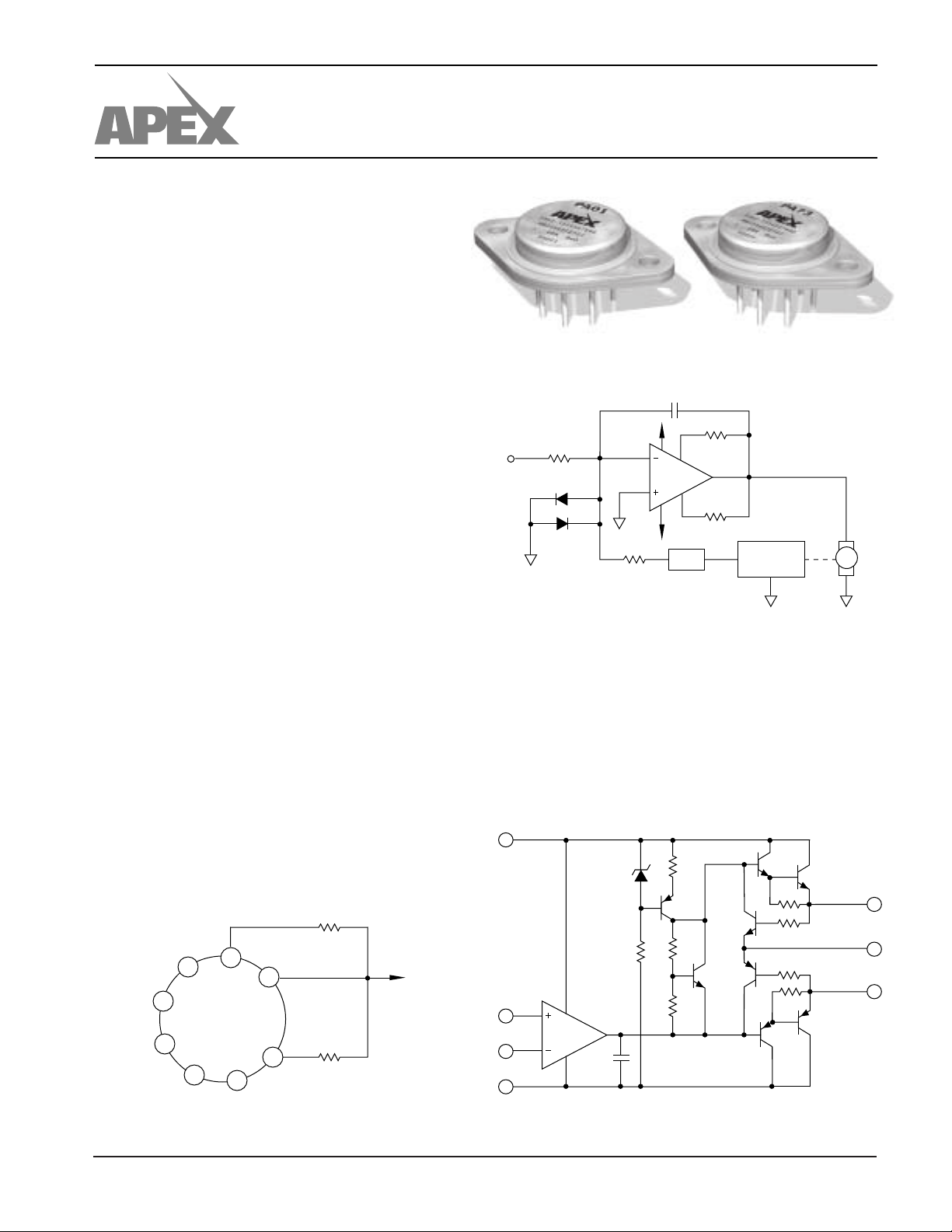
TYPICAL APPLICATION
C
F
R
F/V
0/–5V
*
Q1
*
CL+
.33
Ω
3W
R
CL–
.33
Ω
3W
*
Q4
OPTO
PULSE
GEN.
Q2A
Q3
Q5
*
Q6A
+6V
IN
1N4148
R
IN
PA01
–30V
R
F
V
0/+5V
UNSYMMETRICAL SUPPLIES FOR EFFICIENCY
Unidirectional Optical Speed Control
The pulse output of a non-contact optical sensor drives a
voltage-to-frequency converter which generates feedback for
the op amp. With the loop closed in this manner, the op amp
corrects for any variations in the speed due to changing load.
Because of operation in only one direction, an unsymmetrical
supply is used to maximize efficiency of both power op amp
and power supply. High speed diodes at the input protect the
op amp from commutator noise which may be generated by
the motor.
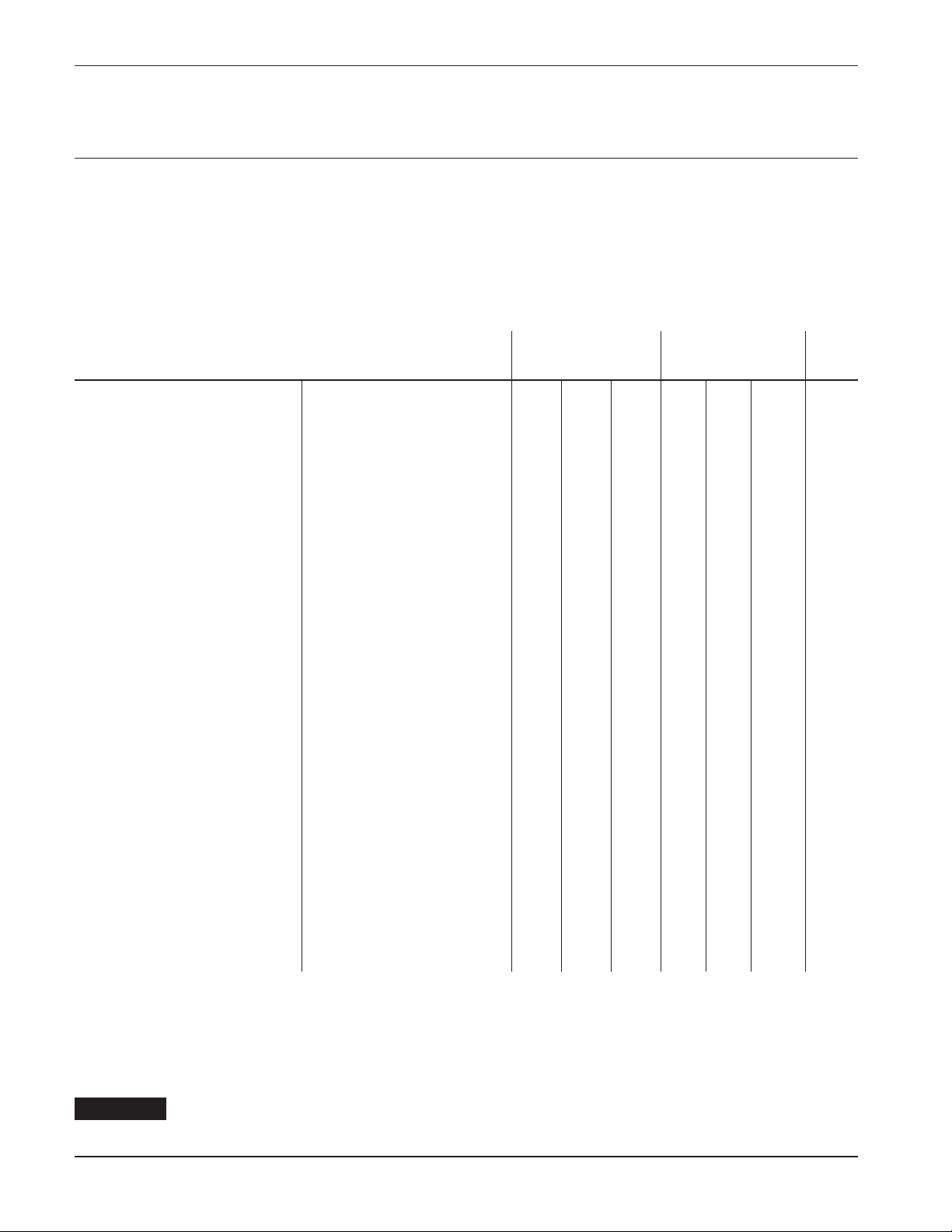
EQUIVALENT SCHEMATIC
3
D1
*
*
4
A1
5
C1
6
NOTE 1: * Indicates not used in PA73. Open base of Q2A connected to
output of A1.
Q2B
Q6B
24V
M
2
1
8
APEX MICROTECHNOLOGY CORPORATION • TELEPHONE (520) 690-8600 • FAX (520) 888-3329 • ORDERS (520) 690-8601 • EMAIL prodlit@apexmicrotech.com
PA01 • PA73
ABSOLUTE MAXIMUM RATINGS
SPECIFICATIONS
PA01 PA73
ABSOLUTE MAXIMUM RATINGS
SUPPLY VOLTAGE, +VS to –V
OUTPUT CURRENT, within SOA 5A 5A
S
60V 68V
POWER DISSIPATION, internal 67W 67W
INPUT VOLTAGE, differential ±VS –3V ±VS –3V
INPUT VOLTAGE, common-mode ±V
TEMPERATURE, junction
1
200°C 200°C
S
±V
S
TEMPERATURE, pin solder -10s 300°C 300°C
TEMPERATURE RANGE, storage –65 to +150°C –65 to +150°C
OPERATING TEMPERATURE RANGE, case –25 to +85°C –25 to +85°C
SPECIFICATIONS
PARAMETER TEST CONDITIONS
PA01
2
MIN TYP MAX MIN TYP MAX UNITS
PA73
INPUT
OFFSET VOLTAGE, initial TC = 25°C ±5 ±12 * ±10 mV
OFFSET VOLTAGE, vs. temperature Full temperature range ±10 ±65 * * µV/°C
OFFSET VOLTAGE, vs. supply TC = 25°C ±35 * ±200 µV/V
OFFSET VOLTAGE, vs. power TC = 25°C ±20 * µV/W
BIAS CURRENT, initial TC = 25°C ±15 ±50 * ±40 nA
BIAS CURRENT, vs. temperature Full temperature range ±.05 ±.4 * * nA/°C
BIAS CURRENT, vs. supply TC = 25°C ±.02 * nA/V
OFFSET CURRENT, initial TC = 25°C ±5 ±15 * ±10 nA
OFFSET CURRENT, vs. temperature Full temperature range ±.01 * nA/°C
INPUT IMPEDANCE, common-mode TC = 25°C 200 * MΩ
INPUT IMPEDANCE, differential TC = 25°C10*MΩ
INPUT CAPACITANCE TC = 25°C3*pF
COMMON MODE VOLTAGE RANGE3Full temperature range ±VS–6 ±VS–3** V
COMMON MODE REJECTION, DC
3
TC = 25°C, VCM = VS –6V 70 110 * * dB
GAIN
OPEN LOOP GAIN at 10Hz Full temp. range, full load 91 113 * * dB
GAIN BANDWIDTH PRODUCT @ 1MHz TC = 25°C, full load 1 * MHz
POWER BANDWIDTH TC = 25°C, IO = 4A, VO = 40V
PHASE MARGIN Full temperature range 45 * °
PP
15 23 * * kHz
OUTPUT
VOLTAGE SWING
VOLTAGE SWING
VOLTAGE SWING
3
3
3
TC = 25°C, IO = 5A ±VS–10 ±VS–5 ±VS–8* V
Full temp. range, IO = 2A ±VS–6 ±VS–5** V
Full temp. range, IO = 46mA ±VS–5* V
CURRENT, peak TC = 25°C ±5* A
SETTLING TIME to .1% TC = 25°C, 2V step 2 * µs
SLEW RATE TC = 25°C, RL = 2.5Ω 1.0 2.6 * * V/µs
CAPACITIVE LOAD, unity gain Full temperature range 3.3 * nF
CAPACITIVE LOAD, gain > 4 Full temperature range SOA *
POWER SUPPLY
VOLTAGE Full temperature range ±10 ±28 ±28 * * ±30 V
CURRENT, quiescent TC = 25°C 20 50 2.6 5 mA
THERMAL
RESISTANCE, AC, junction to case
4
F > 60Hz 1.9 2.1 * * °C/W
RESISTANCE, DC, junction to case F < 60Hz 2.4 2.6 * * °C/W
RESISTANCE, junction to air 30 * °C/W
TEMPERATURE RANGE, case Meets full range specifications –25 25 +85 * * * °C
NOTES: * The specification of PA73 is identical to the specification for PA01 in applicable column to the left.
1. Long term operation at the maximum junction temperature will result in reduced product life. Derate internal power dissipation
to achieve high MTTF.
2. The power supply voltage specified under the TYP rating applies unless otherwise noted as a test condition.
3. +V
4. Rating applies if the output current alternates between both output transistors at a rate faster than 60Hz.
CAUTION
APEX MICROTECHNOLOGY CORPORATION • 5980 NORTH SHANNON ROAD • TUCSON, ARIZONA 85741 • USA • APPLICATIONS HOTLINE: 1 (800) 546-2739
and –VS denote the positive and negative supply rail respectively. Total VS is measured from +VS to –VS.
S
The internal substrate contains beryllia (BeO). Do not break the seal. If accidentally broken, do not crush, machine, or
subject to temperatures in excess of 850°C to avoid generating toxic fumes.

TYPICAL PERFORMANCE
GRAPHS
PA01 • PA73
70
POWER DERATING
60
50
40
30
T = T
C
20
10
0
0 20 40 60 80 100 120
INTERNAL POWER DISSIPATION, P(W)
SMALL SIGNAL RESPONSE
120
100
(dB)
OL
80
T = T
A
TEMPERATURE, T(°C)
60
40
20
0
OPEN LOOP GAIN, A
–20
1 100 10M
10 1K 10K .1M 1M
FREQUENCY, F (Hz)
140
2.8
B
BIAS CURRENT
2.5
2.2
1.9
1.6
1.3
1.0
.7
NORMALIZED BIAS CURRENT, I (X)
–25 25 50 75
–50 0 100
CASE TEMPERATURE, T (°C)
PHASE RESPONSE
0
–30
–60
–90
–120
PHASE, (°)ϕ
–150
–180
–210
10 10K 1M
1 100 .1M 10M
1K
FREQUENCY, F (Hz)
3.5
CURRENT LIMIT
3.0
2.5
LIM
2.0
1.5
R = 0.6CLΩ
R = 0.3CLΩ
1.0
CURRENT LIMIT, I (A)
.5
0
125
C
–50 –25 50 100
025 75
CASE TEMPERATURE, T (°C)
C
125
POWER RESPONSE
100
68
PP
46
O
32
22
15
10
6.8
OUTPUT VOLTAGE, V (V )
4.6
10K 20K 50K .1M
|+V | + |-V | = 60V
SS
30K
FREQUENCY, F (Hz)
70K
COMMON MODE REJECTION
120
100
80
60
40
20
0
1 10K
COMMON MODE REJECTION, CMR (dB)
3
FREQUENCY, F (Hz)
HARMONIC DISTORTION
1
.3
PA73 @
.1
.03
DISTORTION (%)
.01
PA73 @ P
.003
PA01 @ P
100 1K 3K .1M
300 10K 30K
1K 1M
W
= 50mW
= 50m
O
O
P
PA01 @ P
= 32W
O
= 32W
O
FREQUENCY, F (Hz)
.1M10 100
VS = ±28V
RL = 8
Ω
AV = 10
O
–2
–4
OUTPUT VOLTAGE, V (V)
–6
–8
1.3
1.2
(X)
Q
1.1
1.0
NORMALIZED, I
PULSE RESPONSE
8
6
4
V = ±5V, t = 100ns
IN r
PA01
2
0
for PA73∆
0
2 4 6 8 10 12
TIME, t (µs)
QUIESCENT CURRENT
PA01 @ 85
PA01 @
.9
PA73 @
.8
.7
20 80
30 40 50 60 70
TOTAL SUPPLY VOLTAGE, V
°C
–25 to +25
–25 to +85
°C
°C
S
(V)
100
INPUT NOISE
√
70
N
50
40
30
20
10
INPUT NOISE VOLTAGE, V (nV/ Hz)
10 100 10K .1M
1K
FREQUENCY, F (Hz)
+6
OPEN LOOP GAIN
+4
(dB)
+2
OL
0
T = 85
C
–2
NORMALIZED, A
–4
–6
30 80
20 40 50
TOTAL SUPPLY VOLTAGE, V
°C
T =
C
T = 25
C
–25°C
°C
60
70
S
(V)
APEX MICROTECHNOLOGY CORPORATION • TELEPHONE (520) 690-8600 • FAX (520) 888-3329 • ORDERS (520) 690-8601 • EMAIL prodlit@apexmicrotech.com

PA01 • PA73
GENERAL
Please read Application Note 1 "General Operating Considerations" which covers stability, supplies, heat sinking, mounting, current limit, SOA interpretation, and specification interpretation. Visit www.apexmicrotech.com for design tools that
help automate tasks such as calculations for stability, internal
power dissipation, current limit and heat sink selection. The
"Application Notes" and "Technical Seminar" sections contain
a wealth of information on specific types of applications.
Package outlines, heat sinks, mounting hardware and other
accessories are located in the "Packages and Accessories"
section. Evaluation Kits are available for most Apex product
models, consult the "Evaluation Kit" section for details. For the
most current version of all Apex product data sheets, visit
www.apexmicrotech.com.
SAFE OPERATING AREA (SOA)
The output stage of most power amplifiers has three distinct
limitations:
1. The current handling capability of the transistor geometry
and the wire bonds.
2. The second breakdown effect which occurs whenever the
simultaneous collector current and collector-emitter voltage
exceeds specified limits.
3. The junction temperature of the output transistors.
5.0
4.0
3.0
2.0
1.5
1.0
Tc = 85°C
Tc = 125°C
THERMAL
.8
steady state SECOND BREAKDOWN
t = 5ms
t = 0.5ms
t = 1ms
OPERATING
CONSIDERATIONS
1. For sine wave outputs, use Power Design
Make sure the load line does not cross the 0.5ms limit and
that excursions beyond any other second breakdown line
do not exceed the time label, and have a duty cycle of no
more than 10%.
For other waveform outputs, manual load line plotting is
recommended. Applications Note 22, SOA AND LOAD
LINES, will be helpful. A Spice type analysis can be very
useful in that a hardware setup often calls for instruments or
amplifiers with wide common mode rejection ranges.
2. EMF generating or reactive load and short circuits to the
supply rail or shorts to common are safe if the current limits
are set as follows at T
±V
S
C, L, OR EMF LOAD COMMON
= 85°C.
C
SHORT TO ±V
S
34V .58A 1.1A
30V .46A 1.4A
25V .61A 1.7A
20V .86A 2.1A
15V 1.3A 2.9A
3. The output stage is protected against occaisional transient
flyback. However, for protection against sustained, high
energy flyback, external fast-recovery diodes should be
used.
1
to plot a load line.
SHORT TO
CURRENT LIMIT
Proper operation requires the use of two current limit resistors, connected as shown, in the external connection diagram.
The minimum value for R
reliability it should be set as high as possible. Refer to the
“General Operating Considerations” section of the handbook
for current limit adjust details.
is 0.12 ohm; however, for optimum
CL
.6
.4
PA01 LIMIT
.3
10 15 20 25 30 35 40 50 60
The SOA curves combine the effect of these limits. For a
given application, the direction and magnitude of the output
current should be calculated or measured and checked against
the SOA curves. This is simple for resistive loads but more
complex for reactive and EMF generating loads.
1
Note 1. Power Design is a self-extracting Excel spreadsheet
APEX MICROTECHNOLOGY CORPORATION • 5980 NORTH SHANNON ROAD • TUCSON, ARIZONA 85741 • USA • APPLICATIONS HOTLINE: 1 (800) 546-2739
This data sheet has been carefully checked and is believed to be reliable, however, no responsibility is assumed for possible inaccuracies or omissions. All specifications are subject to change without notice.
PA01, 73U REV. O FEBRUARY 2001 © 2001 Apex Microtechnology Corp.
available free from www.apexmicrotech.com
 Loading...