

e
A
E
R
t
e
u
m
r
a
B
e
k
A
u
c
n
e
o
r
r
i
o
R
c
s
C
g
w
o
A
o
V
o
t
t
T
N
APE
B
+
I
S
o
e
n
o
n
a
A
t
h
m
A
s
T
*
N
O
a
e
o
d
e
e
n
a
m
R
g
L
R
t
o
n
(
h
p
a
s
i
P
U
w
p
g
a
s
c
1
2
FEATU
▓
Integrate
▓
Input Vol
▓
Low Thr
▓
Quick O
▓
Over-Te
▓
Over Cu
▓
Short Cir
▓
Open-Dr
▓
Low ON-
▓
Halogen
APPLIC
▓
Telecom
▓
Set-Top-
▓
Consum
▓
Noteboo
dvan
lectro
1.
ES
d 1.5A Singl
age Range:
shold Contr
tput Discha
perature P
rent Protect
cuit Protecti
in Fault Fla
Resistance
Free Produ
ATIONS
Systems
ox
r Electronic
s / Netbook
ed Po
ics C
5A LO
Channel L
0.8V to 5.5
l Input
ge Transist
otection
on
n
g Outpu
ON
s
= 40mΩ
er
rp.
D SWI
ad Switch
r
CH W
DE
The
contr
MOS
rang
conti
contr
of i
sign
ddit
resis
switc
when
ther
The
with
TH CO
CRIPTI
APE8988 i
lled turn
FET that c
of 0.8V
uous curr
lled by an
terfacing
ls.
onal featur
or is added
is turned
the devic
al shutdow
PE8988 is
mallest co
TROL
N
s a low
on. It con
n operate
to 5.5V a
nt up to
n/off input
irectly wit
s include
for output
off. A well
enters h
.
vailable in
ponents.
A
ED T
load s
ON
tains one
ver an in
d support
1.5A. The
EN), which
low-volta
a 330Ω on
quick disch
rotection i
rd short
mall SOT-2
E8988
RN-ON
itch with
N-channel
ut voltage
maximum
switch is
is capable
e control
-chip load
rge when
equipped
ircuit and
6 package
TYPIC
L APPLI
V
IN
CATION
IN
1
uF
VIN
EN
V
G
5V
IAS
8988
D
FLG
VOU
Option for fl
F
10kΩ~100kΩ
*R
1
10kΩ
V
OUT
C
OUT
0.1uF
a
transient filter
ng
FLAG
*C
1
0.1uF
Data and sp
cifications s
bject to chan
e without no
ice
2
0131015V1.

A
E
8
U
e
p
e
M
e
T
c
n
A
k
X
R
D
e
w
o
e
R
e
t
A
)
M
S
R
C
C
V
+
V
t
°
°
°
O
V
V
°
DFLG
T
S
B
P
2
ORDER
APE89
ABSOL
VIN
VBIAS
VOUT
dvan
lectro
ING / P
X
Pac
Y: S
TE MA
ed Po
ics C
CKAGE
age Typ
OT-26
IMUM
er
rp.
INFOR
ATING
ATION
(at TA=25°
-0.3
-0.3
VIN
)
to 6V
to 6V
0.3V
GN
op View
OT-26
VBIAS
6
(Mark ing)
1
VIN VOUT
EN
5
4
23
A
E8988
EN, /FLG
Storage Te
Junction T
Lead Tem
Thermal R
RECO
VIN
VBIAS
VOUT
CIN
Junction T
Operating
mperature
mperature (
erature (Sol
sistance fro
MENDE
mperature (
emperatur
ange (TST)
TJ)
dering, 10s
m Junction
OPER
TJ)
Range (T
A
c.)
o Ambient (
SOT-26
TING
-0.3
-65
150
260
θJA)
250
ONDITI
0.8
. V
0.≧
-40°
4.5
IN
125
to 6V
o +150°C
C
C
C/W
NS
to 5.5V
to 5.5V (V
1uF
C
C to 85°C
IAS≧VIN)

A
E
R
o
P
C
C
a
R
m
-
y
R
e
o
c
n
P
=
R
s
e
e
e
w
o
A
F
o
u
oas
n
f
t
O
U
0
N
e
A
f
P
A
5
4
5
5
0
3
ELECT
(VIN=0.8V t
Quiescent
Shutdown
Under-Volt
Switch ON
Current Li
VOUT Rise
Output Pull
FLAG Dela
dvan
lectro
ICAL S
5.5V, V
ARAMETE
urrent
urrent
ge Lockout
esistance
it Threshold
Time
Down Resi
Time
BIAS
(Note1)
ed Po
ics C
ECIFIC
5V, CIN=1u
tance
er
rp.
TIONS
, C
=0.1
OUT
SYM
I
V
BIAS
ISD V
V
T
UVLO
V
H
HYS
RON V
ILM
tSS V
R
V
OPD
t
DELAY
, TA =25°C
TEST C
=5V, I
EN
=GND
EN
hreshold
ysteresis
EN=VBIAS
=5V
IN
=5V, VEN=
IN
m fault con
fr
sert
, unless oth
=
0A
OUT
, I
=200mA
O
T
V
dition to FL
NDITION
rwise speci
MIN
3.0
1.8
G
ied)
TYP M
30
3.6
0.4
40
650
330 4
3
A
E8988
UNIT
0 uA
1 uA
.2 V
V
0 mΩ
A
us
00 Ω
ms
FLAG ON
EN Input L
EN Thresh
Thermal Sh
Note1: Gua
esistance
akage Curr
ld
utdown Thr
rantee by d
nt
(Note1)
shold
sign, not pr
R
FLG
IEN V
VIH o
VIL o
TSD
H
duction tes
=5V or G
EN
f
ysteresis
ed.
D
1.6
20
140
30
0 Ω
1 uA
V
.6 V
o
C
o
C
A
E
S
c
n
O
GVVOEVB/F
A
UOsTh
o
r
w
o
G
I
S
S
B
O
r
u
e
f
r
v
p
C
n
a
P
4
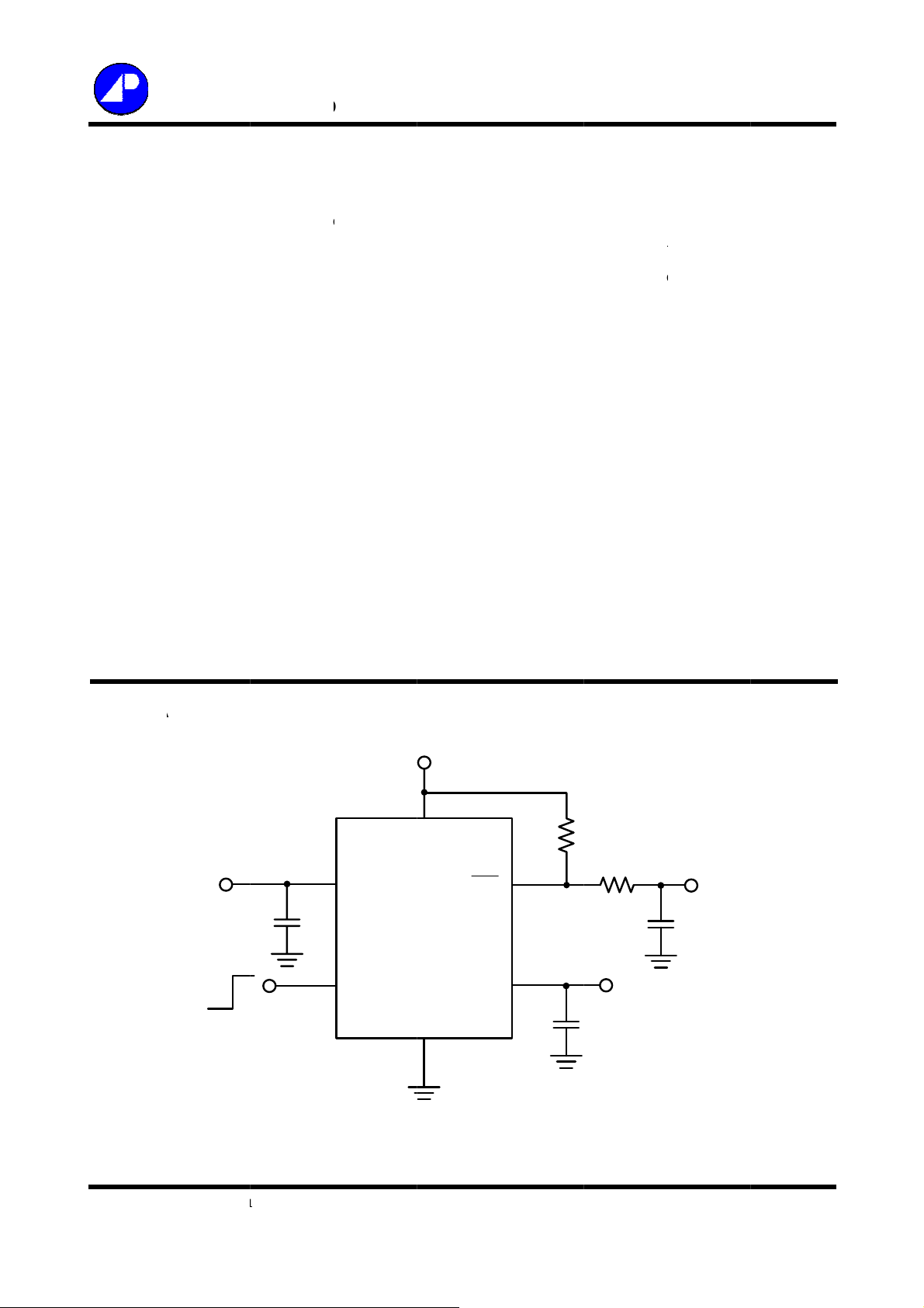
PIN DE
PIN No.
1
2
3
4
5
6
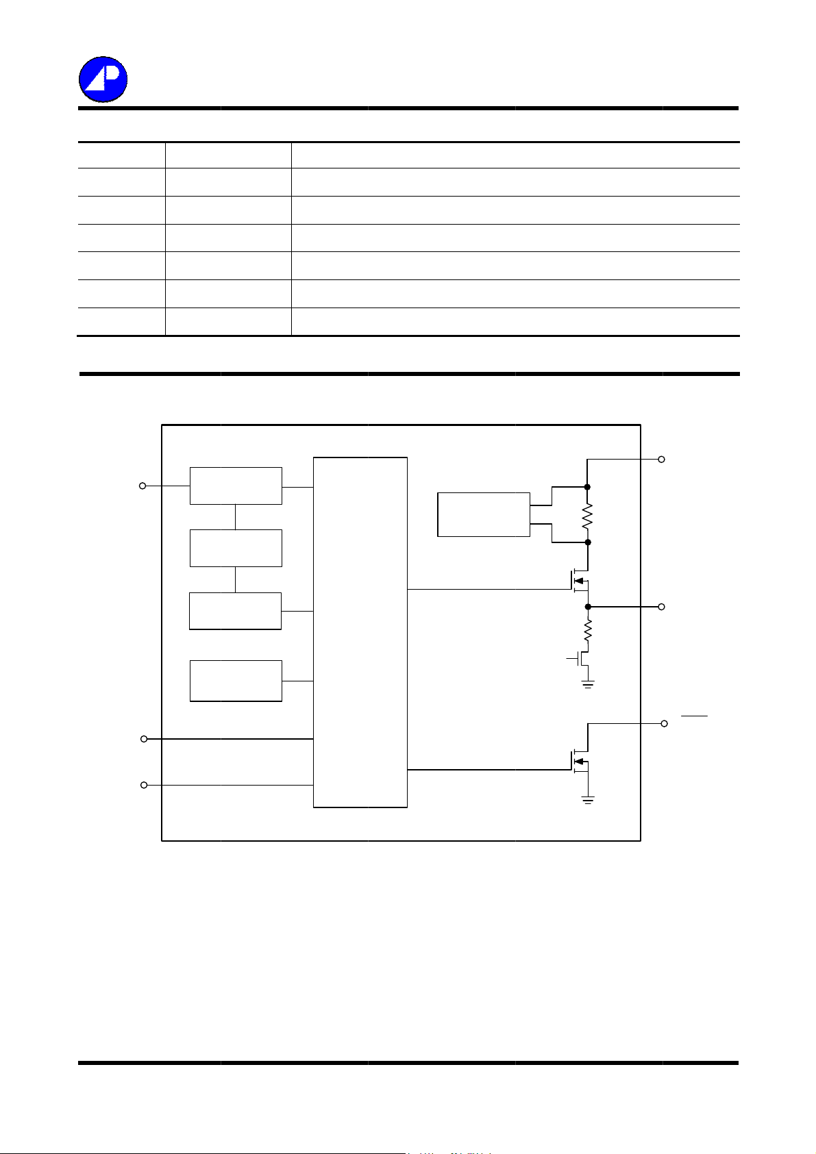
BLOCK
dvan
lectro
CRIPTI
PIN S
DIAGR
ed Po
ics C
NS
YMBOL
ND
IN
UT
N
IAS
LG
M
er
rp.
round.
nput Power
witch outp
witch contr
ias Voltag
pen-drain
Supply.
t.
ol input, acti
.
ault flag out
PIN DES
e high. Do
ut.
RIPTION
ot leave flo
ting.
A
E8988
VIN
VBIAS
EN
GND
Cha
Pr
VLO
cillato
ge Pump
ermal
tection
Cont
Logi
Current
Limiting
VOUT
ol
c
Output D i
scharge
FLG

A
E
A
O
5
c
n
O
o
R
R
R
w
o
C
V
V
V
V
R
U
G
T
T
T
p
p
p
P
5
TYPIC
CIN=1µF, C
Fig.
dvan
lectro
L PERF
=0.1µF, I
UT
1 Turn-on
ed Po
ics C
RMAN
=0A, ch1:
esponse,
er
rp.
E CHA
, ch2: V
EN
IN=0.8V
ACTER
, ch3: /FL
O
T
ISTICS
, ch4: IIN
Fig.2
urn-on Res
onse, VIN=
A
E8988
1.2V
3 Turn-on
Fig.
Turn-on
Fig.
esponse,
esponse,
IN=1.5V
IN=3.3V
Fig.4
Fig.6
urn-on Res
urn-on Res
onse, VIN=
onse, VIN=
1.8V
5.0V

A
E
A
gFig
V
c
n
O
f
N
,
w
o
C
a
3
3
R
0
0
t
R
(us) tF(us)
ILM(A)
C
0
4
t
R
(us)
u
4
tF(us)
2
ILM(A)
d
e
a
V
F
V
F
2
J
P
V
V
r
6
=
6
TYPIC
500
450
400
350
300
(us)
250
D-ON
t
200
150
100
50
0
5.0
4.5
4.0
3.5
3.0
(us)
2.5
2.0
D-OFF
t
1.5
1.0
0.5
0.0
dvan
lectro
L PERF
Cin=1uF, Cout
1.4 2.0
0.8
Fi
.7 Turn-on
1.4 2.0
0.8
ed Po
ics C
RMAN
=0.1uF, Io=0A
2.6 3.2
VIN (V)
Delay Time
2.6 3.2
VIN (V)
er
rp.
E CHA
.8 4.4 5.
vs. VIN
.8 4.4 5.
ACTER
0
ISTICS
700
Cin=1
600
500
400
300
200
100
0
0.8 1.
Fig.8
1000
Cin=1
950
900
850
800
750
700
650
600
0.8 1.
(
ontinue
F, Cout=0.1u
2.0 2.6
VOUT Ris
uF, Cout=0.1u
2.0 2.6
)
, Io=0A
3.2 3.8
IN (V)
Time vs.
, Io=0A
3.2 3.8
IN (V)
A
4.4 5.0
IN
4.4 5.0
E8988
.9 Turn-of
60
BIAS=VIN=5V
55
50
45
(mΩ)
40
ON
R
35
30
25
20
-20 0 2
-40
Fig.11 R
Delay Time
Io=1A
04060
T
(°C)
J
vs. Temper
O
vs. VIN
80 100 12
ture
3.0
2.7
2.4
2.1
1.8
1.5
1.2
0.9
0.6
0.3
0.0
-40 -
Fig.12
Fig.1
VOUT F
00
Current Limi
ll Time vs.
VBIAS
040
T
(°C)
t vs. Tempe
IN
VIN=5V
080
ature

A
E
A
0
0
c
n
O
r
a
w
o
C
Te
T
R
V
EN
(V)
I
BIAS
(uA)
C
E
V
-
V
EN
(V)
I
BIAS
(uA)
d
d
n
2
T
4
P
e
6
V
V
7
TYPIC
4.5
4.0
3.5
3.0
2.5
(V)
2.0
BIAS
V
1.5
1.0
0.5
0.0
Fig.13
3.5
dvan
lectro
L PERF
-20 0
-4
UVLO Th
ed Po
ics C
RMAN
20 40
T
(°C)
J
eshold vs.
er
rp.
E CHA
UVLO-H
UVLO-L
60 80
mperature
ACTER
ISTICS
2.0
1.8
1.6
1.4
1.2
1.0
0.8
0.6
0.4
0.2
0.0
-40
Fig.14
45
(
ontinue
20 0
N Threshol
)
040
(°C)
J
A
vs. Tempe
E8988
VEN-H
VEN-L
080
rature
3.0
2.5
2.0
1.5
1.0
FLAG Delay Time (ms)
0.5
0.0
-4
Fig.15
-20 0
FLAG Del
20 40
T
(°C)
J
y Time vs.
60 80
emperature
40
35
30
25
20
15
10
5
0
-40 -20
Fig.16
020
BIAS Curre
06080
T
(°C)
J
t vs. Temp
IN=0.8V
IN=5V
100 120
rature

A
E
n
w
1
T
s
T
c
9
p
h
e
a
n
p
C
c
n
N
t
w
D
e
a
s
e
d
s
c
e
h
e
w
o
A
e
a
t
o
d
b
v
o
T
w
h
o
%
G
h
m
d
e
h
s
n
W
w
t
d
d
h
e
0
o
a
U
c
n
v
d
h
P
o
2
c
n
e
8
t
V
p
y
t
t
S
s
APPLIC
On/Off Co
The load s
capable of
GPIO logic
The Figure
t
: VOU
D-ON
tR: VOUT ri
t
: VOU
D-OFF
tF: VOUT fa
dvan
lectro
ATION I
trol
itch is con
interfacing
threshold.
7 shows th
turn-on del
e time
turn-off de
ll time
ed Po
ics C
FORM
rolled by th
ith low volt
o not leave
VOUT on/
y time
lay time
EN
er
rp.
TION
EN pin. T
ge signals.
he EN pin fl
ff definition.
e EN pin i
The EN pi
at.
90%
active hig
can be us
and has a
d with stan
9
%
low thresh
dard 1.8V,
A
E8988
ld making i
.5V or 3.3
FLAG Indi
The APE8
resistor. Ty
monitors t
condition k
Input Cap
An input ca
supply duri
Output Ca
Setting a
switch, this
removed.
ator
88 provide
ically conn
e fault con
eps for 3m
citor
pacitor is re
g high curr
acitor
greater t
IN
prevents th
VOUT
an error in
ct to +5V
ition for o
, /FLG beco
ommended
nt applicati
an the C
current flo
OU
t
D-ON
Fig.17
icator (/FL
ias supply t
er current,
mes low im
to be place
n.
is highly r
s through t
10
t
R
ON/OFF
) output,
rough a 10
short circui
ediately.
between V
commende
e body dio
t
D-OFF
aveform
hich is an
kΩ resistor.
and therm
IN and GND
. Since the
e from VO
10%
t
F
pen-drain o
The FLAG
l shutdow
to limit the
internal bo
T to VIN w
utput requiri
omparator
conditions.
oltage drop
y diode is i
en the syst
ng a pull-u
ontinuousl
If the faul
on the inpu
the NMO
m supply i

A
E
n
b
h
p
c
n
N
s
e
u
w
o
A
B
N
s
c
d
c
)
e
e
d
e
T
o
o
f
n
P
e
a
9
e
APPLIC
Layout Co
Follow the
1. Keep t
2. The in
inducta
dvan
lectro
ATION I
sideration
elow guidel
e high curr
ut and outp
nces.
ed Po
ics C
FORM
ines for PC
nt paths (VI
t capacitor
er
rp.
TION
layout to a
, VOUT an
should be
(C
ontinued
hieve stabl
GND) wid
lose to the
operation.
and short t
evice as p
ake below
obtain the
ssible to mi
igure for ref
best effect.
imize the p
A
E8988
rence.
rasitic trac
Fig.18
Referenc
layout

A
E
N
P
c
n
w
o
e
2
2
2
2
e
0
0002
0
0
P
0
MARKI
SOT-26
H
dvan
lectro
G INFO
SS
ed Po
ics C
RMATIO
Part
Dat
SS:
SS:
SS:
SS:
er
rp.
N
Number : HP
Cod
004, 2008, 2
003, 2007, 2
, 2006, 2
001, 2005, 2
12…
11...
10…
09...
A
E8988
1

 Loading...