

Advanced Power
Electronics Corp.
1A ULTRA LOW DROPOUT LINEAR REGULATOR
FEATURES DESCRIPTION
Ultra Low Dropout - 0.2V(typical) at 1A Output Current
Low ESR Output Capacitor (Multi-layer Chip
Capacitors (MLCC)) Applicable
0.8V Reference Voltage
Fast Transient Response
Adjustable Output Voltage by External Resistors
Power-On-Reset Monitoring on Both VCNTL and VIN Pins
Internal Soft-Start
Under-Voltage Protection
Current-Limit and Thermal Shutdown Protection
Power-OK Output with a Delay Time
ESOP-8, SOT-26 and DFN 2x2 Pb-Free Packages.
The APE8901 is a 1A ultra low dropout linear
regulator. This product is specifically designed to provide
well supply voltage for front-side-bus termination on
motherboards and NB applications. The IC needs two
supply voltages, a control voltage for the circuitry and a
main supply voltage for power conversion, to reduce
power dissipation and provide extremely low dropout. The
APE8901 integrates many functions. A Power-On-Reset
(POR) circuit monitors both supply voltages to prevent
wrong operations. A thermal shutdown and current limit
functions protect the device against thermal and current
over-loads. A POK indicates the output status with time
delay which is set internally. It can control other converter
for power sequence. The APE8901 can be enabled by
other power system. Pulling and holding the EN pin below
0.3V shuts off the output.
The APE8901 is available in ESOP-8, SOT-26 and
DFN 2x2 packages. That features small size as SOP-8
with an Exposed Pad to reduce the junction-to-case
resistance, being applicable in 2~3W applications.
APE8901
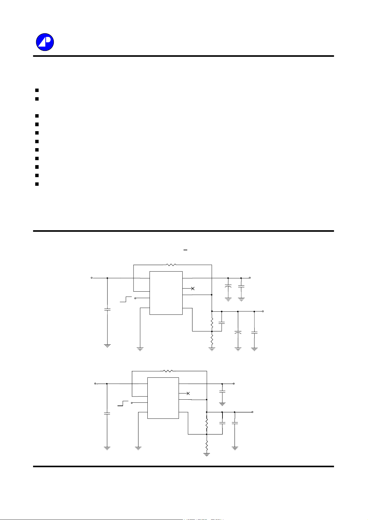
TYPICAL APPLICATION CIRCUIT
1. Using an Output Capacitor with ESR > 20mΩ
VCNTL=5V
ON
OFF
C1
1uF
2. Using an MLCC as the Output Capacitor
VCNTL=5V
ON
OFF
C1
1uF
U1
VCNTL
POK
EN
GND
APE8901
U2
VCNTL
POK
EN
GND
APE8901
R3
1K
R3
1K
VOUT
VIN
NC
VOUT
VIN
NC
FB
C3
C4
220uF
VIN=1.5V
VIN=1.5V
Vout=1.2V/1A
C5
0.1u
Vout=1.2V/1A
C2
100uF
0.1uF
FB
R1
39K
R1
1K
R2
2K
22uF
56pF
C3
C6
C6
12~48nF
C5
22u
VOUT=VFB*(1+R1/R2)
VFB = 0.8V
Data and specifications subject to change without notice
R2
78K
1
200906252
Advanced Power
-
-
-
-
-
-
-
Electronics Corp. APE8901
ABSOLUTE MAXIMUM RATINGS (at T
VCNTL Supply Voltage (V
VIN Supply Voltage (V
EN & FB Pin Voltage (VI/O) ----------------------------Power Voltage (V
Power Dissipation (P
) -------------------------------------- -0.3V to 7V
POK
)
D
Storage Temperature Range (T
Junction Temperature Range (T
Operating Temperature Range (T
Thermal Resistance Junction to Ambient (Rth
Thermal Resistance Junction to Case (Rth
) -------------------------- -0.3V to 7V
CNTL
) ---------------------------------- -0.3V to 6V
IN
-0.3V to VCNTL+0.3V
ESOP-8 ------ 3W
SOT-26 -----DFN 2x2 -----
) --------------------- -65°C To 150°C
ST
) ---------------------- -40°C To 125°C
J
) ------------------ -40°C To 85°C
OP
0.4W
0.8W
)
ja
ESOP-8 ------ 40°C/W
SOT-26 -----DFN 2x2 -----
jc
250°C/W
125°C/W
)
ESOP-8 ------ 15°C/W
SOT-26 -----DFN 2x2 -----
180°C/W
20°C/W
=25oC)
A
Note. Rth
is measured with the PCB copper area (need connect to Expose-Pad) of approximately 1.5 in2 (Multi-layer) by ESOP-8 and DFN-8L packages.
ja
RECOMMENDED OPERATING CONDITIONS
V
Supply Voltage (VCNTL) -------------------------- 3V to 6V
CNTL
VIN Supply Voltage (V
Output Voltage (V
Output Current (I
) ---------------------------------- 1V to 5.5V
IN
) -------(V
OUT
) -------------------------------------- 0 to 1A
OUT
CNTL-VOUT
> 1.9V)---- 0.8V to 2.8V
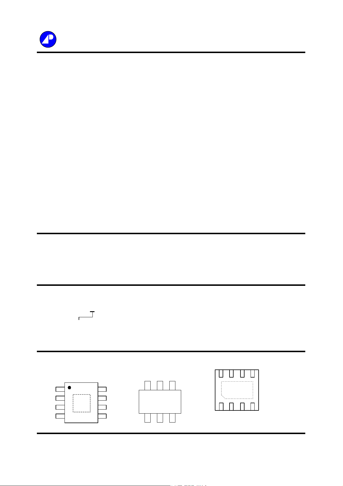
ORDERING INFORMATION
APE8901X
Package Type
MP : ESOP-8
Y : SOT-26
GN2 : DFN 2x2
PACKAGE INFORMATION
POK
VIN
VCNTL
(
1
2
3
4
ESOP-8
Top View
AX5913
GND
)
8
GND
7
FBEN
6
VOUT
5
NC
EN
6
123
FB
VCNTL
VIN
5
( Top View )
SOT-26
GND
4
VOUT
GND
POK
VOUT
78
GND
12 3
EN
DFN 2x2
(TOP VIEW)
VIN
NCFB
56
4
VCNTL
2
Advanced Power
Electronics Corp. APE8901
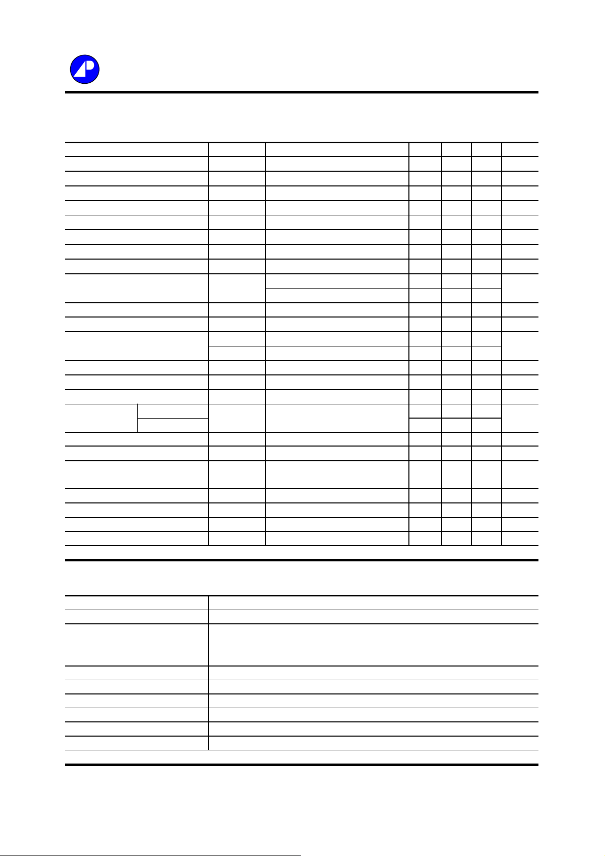
ELECTRICAL SPECIFICATIONS
(V
= 5V, VIN = 1.5V, V
CNTL
= 1.2V, TA=25oC unless otherwise specified)
OUT
Parameter SYM TEST CONDITION MIN TYP MAX
VCNTL POR Threshold V
VCNTL POR Hysteresis V
VIN POR Threshold V
VIN POR Hysteresis V
VCNTL Nominal Supply Current I
VCNTL Shuntdown Current I
Feedback Voltage V
CNTL
CNTL(hys)
IN
IN(hys)
CNTL
SD
FB
Load Regulation I
Dropout Voltage
V
DROP
EN= V
CNTL
EN= 0V - 10 30 uA
V
=3 ~ 6.0V 0.784 0.8 0.816 V
CNTL
=0A ~ 1A - 0.06 0.25 %
OUT
V
<2.0V,I
OUT
2.0V<V
=1A - 200 250
OUT
OUT
<2.8V,I
=1A - 250 300
OUT
2.5 2.7 2.9 V
- 0.4 - V
0.8 0.9 1 V
- 0.5 - V
0.4 1 2 mA
UNITS
mV
VOUT Pull Low Resistance EN=0V - 90 120 Ω
Soft Start Time T
EN Pin Logic High Threshold Voltage
SS
V
ENH
V
ENL
Enable 1.2 - -
Disable - - 0.4
-2-mS
V
EN Hysteresis -50-mV
EN Pin Pull-Up Current I
Current Limit I
V
Ripple Rejection
V
IN
CNTL
PSRR dB
EN
LIM
EN=GND - 10 - uA
125℃ 1.2 - - A
F=120Hz, I
=100mA
OUT
-70-
-65-
Under-Voltage Threshold VFB Falling - 0.4 - V
POK Threshold Voltage for Power OK V
POK Threshold Voltage for Power
Not OK
V
POK
PNOK
VFB Rising 89% 92% 95% VFB
VFB Falling 78%
81% 84% VFB
POK Low Voltage POK sinks 5mA - 0.25 0.4 V
POK Delay Time T
DELAY
0.8 2 10 mS
Thermal Shutdown Temp TSD - 150 - °C
Thermal Shutdown Hysteresis - 40 - °C
PIN DESCRIPTIONS
PIN SYMBOL PIN DESCRIPTION
FB
EN
VIN
POK
VCNTL
NC
VOUT
GND
Feedback Pin
Internal Pull High.
EN=High or Floating → Enable
EN=Low → Shutdown Mode
Input voltage.
Power OK Output Pin
CNTL Pin Input Voltage
No connect
Output Voltage
GND Pin.
3
Advanced Power
purp
Electronics Corp. APE8901
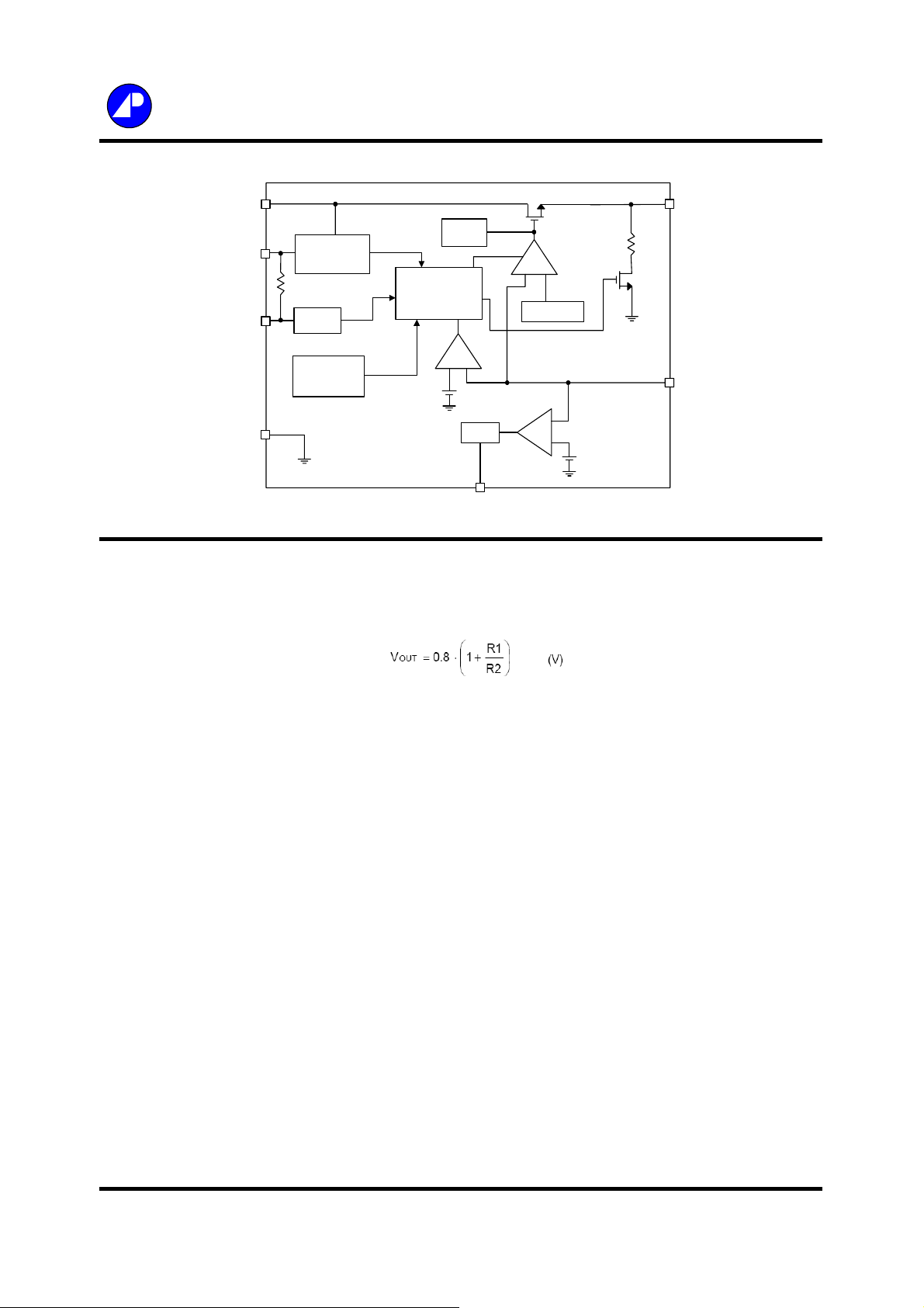
BLOCK DIAGRAM
VIN
VCNTL
EN
GND
PIN DESCRIPTION
FB
Connecting this pin to an external resistor divider receives the feedback voltage of the
regulator. The output voltage set by the resistor divider is determined by:
Power -ON
Reset
Enable
Thermal
Shutdown
Current
Limit
Soft-Start
And
Control Logic
UV
0.4V
-+
Delay
POK
N-MOSFET
-
+
Bandgap
POK
Error
Amp
-+
VOUT
90Ω
FB
90%
Vref
VIN
VCNTL
POK
EN
Where R1 is connected from VOUT to FB with Kelvin sensing and R2 is connected from FB
to GND. A bypass capacitor may be connected with R1in parallel to improve load transient
response. The recommended R2 and R1 are in the range of 1K~100kΩ.
Main supply input pins for power conversions. The voltage at this pin is monitored for
Power-On Reset
ose.
Power input pin of the control circuitry. Connecting this pin to a +5V (recommended) supply
voltage provides the bias for the control circuitry. The voltage at this pin is monitored for Power-On
Reset purpose.
Power-OK signal output pin. This pin is an open-drain output used to indicate status of
output voltage by sensing FB voltage. This pin is pulled low when the rising FB voltage is not
above the VPOK threshold or the falling FB voltage is below the VPOK threshold, indicating the
output is not OK.
Enable control pin. Pulling and holding this pin below 0.4V shuts down the output. When re-
enabled, the IC undergoes a new soft-start cycle. Left this pin open, this pin is internal pulled up to
VCNTL voltage, enabling the regulator.
4

Advanced Power
Electronics Corp. APE8901
PIN DESCRIPTION
VOUT
Output of the regulator. Please connect Pin 6 using wide tracks. It is necessary to connect
an output capacitor with this pin for closed-loop compensation and improving transient responses.
FUNCTION DESCRIPTION
Power-On-Reset
A Power-On-Reset (POR) circuit monitors both input voltages at VCNTL and VIN pins to
prevent wrong logic controls. The POR function initiates a soft-start process after the two supply
voltages exceed their rising POR threshold voltages during powering on. The POR function also
pulls low the POK pin regardless the output voltage when the VCNTL voltage falls below its falling
POR threshold.
Internal Soft-Start
An internal soft-start function controls rise rate of the output voltage to limit the current
surge at start-up. The typical soft-start interval is about 2mS.
Output Voltage Regulation
An error amplifier working with a temperature compensated 0.8V reference and an output
NMOS regulates output to the preset voltage. The error amplifier designed with high bandwidth
and DC gain provides very fast transient response and less load regulation. It compares the
reference with the feedback voltage and amplifies the difference to drive the output NMOS which
provides load current from VIN to VOUT.
Current-Limit
The APE8901 monitors the current via the output NMOS and limits the maximum current to
prevent load and APE8901 from damages during overload or short circuit conditions.
Under-Voltage Protection (UVP)
The APE8901 monitors the voltage on FB pin after soft-start process is finished. Therefore
the UVP is disabling during soft-start. When the voltage on FB pin falls below the under-voltage
threshold, the UVP circuit shuts off the output immediately. After a while, the APE8901 starts a
new soft-start to regulate output.
Thermal Shutdown
A thermal shutdown circuit limits the junction temperature of APE8901. When the junction
temperature exceeds +150°C, a thermal sensor turns off the output NMOS, allowing the device to
cool down. The regulator regulates the output again through initiation of a new soft-start cycle after
the junction temperature cools by 40°C, resulting in a pulsed output during continuous thermal
overload conditions. The thermal shutdown designed
5

Advanced Power
Electronics Corp. APE8901
TYPICAL PERFORMANCE CHARACTERISTICS
3
2.5
2
1.5
1
VCNTL Supply Current (mA)
0.5
0
33.544.555.56
VIN=1 .5V
VOUT=1 .2V
No L oad
VCNTL (V)
VCNTL VS Feedback Voltage
VCNTL Supply Current
0.86
0.84
0.82
0.8
0.78
Feedback Voltage (V)
0.76
0.74
33.544.555.56
VIN=1. 5V
VOUT=1 .2V
Load=100 mA
VCN TL (V)
50
40
30
20
10
VCNTL Shutdown Current (uA)
0
33.544.555.56
VCNTL (V)
Temperature VS VCNTL Supply Current
VCNTL Shutdown Current
4
3.5
3
2.5
2
1.5
1
0.5
VCNTL Supply Current (mA)
0
-40℃ -20℃ 0℃ 25℃ 50℃ 85℃ 105℃ 125℃
VIN=1. 5V
VCNTL= 5V
VOUT=1. 2V
No Lo ad
Temperature (℃)
Load VS Feedback Voltage
0.84
0.83
0.82
0.81
0.8
0.79
Feedback Voltage (V)
0.78
0.77
VIN=1. 5V
VCNTL=5V
VOUT=1 .2V
0.76
33.544.555.56
Load (mA)
600
VCNTL= 5V
500
400
300
200
100
Dropout Voltage (mV)
0
0 200 400 600 800 1000
Load VS Dropout
Load (mA)
VOUT=3 .0V
VOUT=2 .5V
VOUT=1 .8V
VOUT=1 .2V
6

Advanced Power
Electronics Corp. APE8901
TYPICAL PERFORMANCE CHARACTERISTICS
0.85
0.84
0.83
0.82
0.81
0.8
0.79
Feedback Voltage (V)
0.78
0.77
0.76
0.75
Temperature VS Feedback Voltage
-40℃ -20℃ 0℃ 25℃ 50℃ 85℃ 105℃ 125℃
Temp erature (℃ )
VIN=1. 5V
VCNTL =5V
VOUT=1 .2V
Load=10mA
3
2.9
2.8
2.7
2.6
2.5
2.4
VCNTL UVLO (V)
2.3
2.2
2.1
2
Temperatur e VS VCNTL UV LO
Rising
Falling
-40℃ -20℃ 0℃ 25℃ 50℃ 85℃ 105℃ 125℃
Temperature (℃)
Power –ON Load Transient
(VIN=1.5V, VCNTL=5V,VOUT=1.2V,Laod=1A) (VIN=1.5V, VCNTL=5V,VOUT=1.2V,Laod=10m~1A)
V
CNTL
V
OUT
V
OUT
I
IN
Enable –ON
(VIN=1.5V, VCNTL=5V,VOUT=1.2V,Laod=1A)
V
CNTL
V
OUT
I
IN
I
OUT
Enable –OFF
(VIN=1.5V, VCNTL=5V,VOUT=1.2V,No Laod)
V
OUT
7

0
ADVANCED POWER ELECTRONICS CORP.
Package Outline : SOT-26
G
L
A
L
C
D
Millimeters
SYMBOLS
A 2.70 2.90 3.10
B 2.60 2.80 3.00
C 1.40 1.60 1.80
B
D 0.30 0.43 0.55
E 0.00 0.05 0.10
H 1.20REF
G
I
J
L
MIN NOM MAX
1.90REF
0.12REF
0.37REF
0.95REF
H
E
I
1.All Dimension Are In Millimeters.
J
2.Dimension Does Not Include Mold Protrusions.
Part Marking Information & Packing : SOT-26
Part Number : H3
H3SS
Date Code
SS:2004,2008,2012…
:2003,2007,2011…
SS
S
S:2002,2006,2010…
SS
:2001,2005,2009…
Draw No. M1-Y-6-G-v0

ADVANCED POWER ELECTRONICS CORP.
Package Outline : DFN 2x2
SYMBOLS
A
A1
b
C
D
D2
E
E2
e
L
y
Millimeters
MIN NOM MAX
0.77 0.90 1.03
0.00 0.015 0.03
0.18 0.23 0.28
0.203 REF
1.95 2.00 2.05
0.55 0.60 0.65
1.95 2.00 2.05
1.15 1.20 1.25
__ 0.50 __
0.3 0.35 0.4
0 __ 0.03
1.All Dimension Are In Millimeters.
2.Dimension Does Not Include Mold Protrusions.
Part Marking Information & Packing : DFN 2x2
H3
XXX
Part Number
Date Code
Draw No. I1-xx-8-G-v00

ADVANCED POWER ELECTRONICS CORP.
Q
Package Outline : ESOP-8
P
B
A2
Millimeters
SYMBOLS
A 5.80 6.00 6.20
B 4.80 4.90 5.00
C 3.80 3.90 4.00
D 0°4°8°
E 0.40 0.65 0.90
F 0.19 0.22 0.25
M 0.00 0.08 0.15
H
L 1.35 1.55 1.75
J
K
G
P 2.15 2.25 2.35
Q 2.15 2.25 2.35
MIN NOM MAX
0.35 0.42 0.49
0.375 REF.
45°
1.27 TYP.
L
I
J
1.All Dimension Are In Millimeters.
2.Dimension Does Not Include Mold Protrusions.
Part Marking Information & Packing : ESOP-8
8901MP
YWWSSS
Package Code
Date Code (YWWSSS)
Y:Last Digit Of The Year
WW:Week
SSS:Sequence
Draw No. M1-MP-8-G-v01

 Loading...