

T
AP4500GM
Pb Free Plating Product
Advanced Power N AND P-CHANNEL ENHANCEMEN
Electronics Corp. MODE POWER MOSFET
▼
▼ Simple Drive Requirement
▼ ▼
▼
▼ Low On-resistance R
▼ ▼
▼
▼ Fast Switching I
▼ ▼
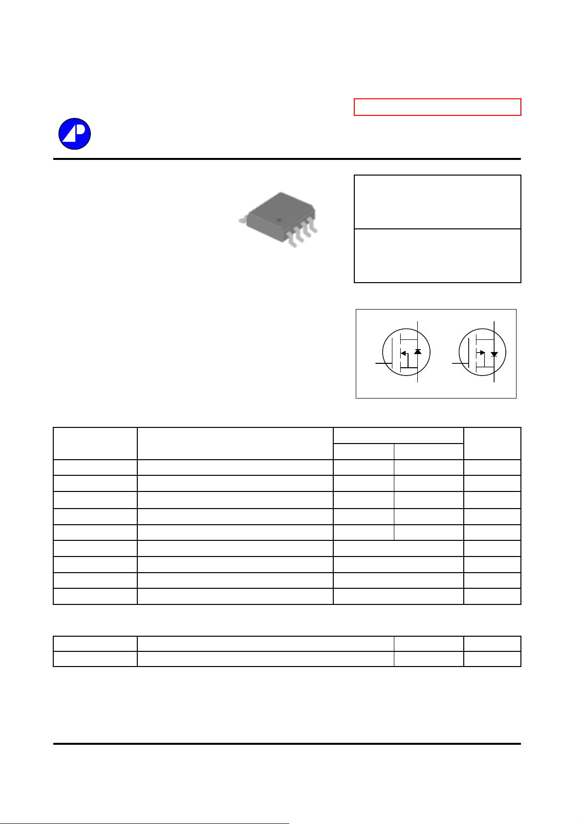
D1
D2
D1
SO-8
D2
G2
S2
G1
S1
Description I
The Advanced Power MOSFETs from APEC provide the
designer with the best combination of fast switching,
ruggedized device design, low on-resistance and costeffectiveness.
N-CH BV
D
P-CH BV
R
D
DSS
DS(ON)
DSS
DS(ON)
D1
20V
30mΩ
6A
-20V
50mΩ
-5A
D2
The SO-8 package is universally preferred for all commercial-
G1
G2
industrial surface mount applications and suited for low voltage
applications such as DC/DC converters.
S1
Absolute Maximum Ratings
Symbol Parameter Rating Units
N-channel P-channel
V
DS
V
GS
I
=25℃ Continuous Drain Current
D@TA
=70℃ Continuous Drain Current
I
D@TA
I
DM
P
=25℃ Total Power Dissipation 2.0 W
D@TA
Drain-Source Voltage -20 V
Gate-Source Voltage ±12 V
Pulsed Drain Current
3
3
1
20
±12
6
4.8
20
-5 A
-4 A
-20 A
Linear Derating Factor 0.016 W/℃
T
STG
T
J
Storage Temperature Range -55 to 150 ℃
Operating Junction Temperature Range -55 to 150 ℃
Thermal Data
Symbol Value Unit
Rthj-a Thermal Resistance Junction-ambient
Parameter
3
Max. 62.5 ℃/W
S2
Data and specifications subject to change without notice
200609031
AP4500GM
N-CH Electrical Characteristics@Tj=25oC(unless otherwise specified)
Symbol Parameter Test Conditions Min. Typ. Max. Units
BV
ΔBV
R
DS(ON)
V
GS(th)
g
fs
I
DSS
I
GSS
Q
g
Q
gs
Q
gd
t
d(on)
t
r
t
d(off)
t
f
C
iss
C
oss
C
rss
DSS
DSS
/ΔT
Drain-Source Breakdown Voltage VGS=0V, ID=250uA 20 - - V
Breakdown Voltage Temperature Coefficient Reference to 25℃, I
j
=1mA - 0.037 -V/℃
D
Static Drain-Source On-Resistance2VGS=4.5V, ID=6A - - 30 mΩ
V
=2.5V, ID=5.2A - - 45 mΩ
GS
Gate Threshold Voltage VDS=VGS, ID=250uA 0.5 - 1.2 V
Forward Transconductance VDS=10V, ID=6A - 18.5 - S
Drain-Source Leakage Current (Tj=25oC)
Drain-Source Leakage Current (Tj=70oC)
VDS=20V, VGS=0V - - 1
VDS=16V, VGS=0V - - 25
Gate-Source Leakage VGS=±12V - Total Gate Charge
2
ID=6A - 9 15
Gate-Source Charge VDS=10V - 1.8 Gate-Drain ("Miller") Charge VGS=4.5V - 4.2 Turn-on Delay Time
2
VDS=10V - 29 Rise Time ID=1A - 65 Turn-off Delay Time RG=6Ω,VGS=4.5V - 60 -
Fall Time RD=10Ω -50Input Capacitance VGS=0V - 300 480
Output Capacitance VDS=8V - 255 Reverse Transfer Capacitance f=1.0MHz - 115 -
±100
uA
uA
nA
nC
nC
nC
ns
ns
ns
ns
pF
pF
pF
Source-Drain Diode
Symbol Parameter Test Conditions Min. Typ. Max. Units
V
SD
t
rr
Q
rr
Forward On Voltage
Reverse Recovery Time IS=6A, VGS=0V, - 26 Reverse Recovery Charge dI/dt=100A/µs - 17 -
2
IS=1.7A, VGS=0V - - 1.2 V
ns
nC
AP4500GM
P-CH Electrical Characteristics@Tj=25oC(unless otherwise specified)
Symbol Parameter Test Conditions Min. Typ. Max. Units
BV
ΔBV
R
DS(ON)
V
GS(th)
g
fs
I
DSS
I
GSS
Q
g
Q
gs
Q
gd
t
d(on)
t
r
t
d(off)
t
f
C
iss
C
oss
C
rss
DSS
DSS
/ΔT
Drain-Source Breakdown Voltage VGS=0V, ID=250uA -20 - - V
Breakdown Voltage Temperature Coefficient Reference to 25℃, I
j
=-1mA - -0.037 -V/℃
D
Static Drain-Source On-Resistance2VGS=-4.5V, ID=-2.2A - - 50 mΩ
V
=-2.5V, ID=-1.8A - - 90 mΩ
GS
Gate Threshold Voltage VDS=VGS, ID=-250uA -0.5 - -1 V
Forward Transconductance VDS=-10V, ID=-2.2A - 2.5 - S
Drain-Source Leakage Current (Tj=25oC)
Drain-Source Leakage Current (Tj=70oC)
Gate-Source Leakage VGS=-Total Gate Charge
2
VDS=-20V, VGS=0V - - -1
VDS=-16V, VGS=0V - - -25
± 12V ±100
ID=-5A - 14 20
Gate-Source Charge VDS=-16V - 2 Gate-Drain ("Miller") Charge VGS=-4.5V - 5.6 Turn-on Delay Time
2
VDS=-10V - 10 Rise Time ID=-2.2A - 11 Turn-off Delay Time RG=6Ω,VGS=-10V - 58 Fall Time RD=4.5Ω -38Input Capacitance VGS=0V - 940 1500
Output Capacitance VDS=-20V - 400 Reverse Transfer Capacitance f=1.0MHz - 160 -
uA
uA
nA
nC
nC
nC
ns
ns
ns
ns
pF
pF
pF
Source-Drain Diode
Symbol Parameter Test Conditions Min. Typ. Max. Units
V
SD
t
rr
Q
rr
Forward On Voltage
Reverse Recovery Time IS=-2.2A, VGS=0V, - 25 Reverse Recovery Charge dI/dt=100A/µs - 21 -
Notes:
1.Pulse width limited by Max. junction temperature.
2.Pulse width <
3.Surface mounted on 1 in
300us , duty cycle <2%.
2
copper pad of FR4 board ; 135℃/W when mounted on Min. copper pad.
2
IS=-1.8A, VGS=0V - - -1.2 V
ns
nC

AP4500GM
N-Channel
25
25
T
=25oC
A
20
4.5V
3.5V
3.0V
2.5V
15
, Drain Current (A)
10
D
I
=2.0V
V
5
0
012345
GS
VDS , Drain-to-Source Voltage (V)
T
=150oC
A
20
15
10
, Drain Current (A)
D
I
5
0
012345
VDS , Drain-to-Source Voltage (V)
4.5V
3.5V
3.0V
2.5V
=2.0V
V
GS
Fig 1. Typical Output Characteristics Fig 2. Typical Output Characteristics
1.8
ID=6A
1.6
V
=4.5V
GS
1.4
DS(ON)
1.2
1.0
Normalized R
0.8
)
Ω
Ω
Ω
Ω
(m
R
DS(ON)
45
40
35
30
25
ID=6A
T
A
=25oC
20
2345
VGS (V)
0.6
-50 0 50 100 150
Tj , Junction Temperature (oC)
Fig 3. On-Resistance v.s. Gate Voltage Fig 4. Normalized On-Resistance
v.s. Junction Temperature
100.00
10.00
1.00
(A)
S
I
0.10
0.01
0.1 0.3 0.5 0.7 0.9 1.1 1.3 1.5
Tj=25oCTj=150oC
VSD (V)
1.5
1
(V)
GS(th)
V
0.5
0
-50 0 50 100 150
Tj ,Junction Temperature ( oC)
Fig 5. Forward Characteristic of Fig 6. Gate Threshold Voltage v.s.
Reverse Diode Junction Temperature

N-Channel
DC
I
f
6
5
4
AP4500GM
1000
=6A
D
V
=10V
DS
=1.0MHz
Ciss
3
2
, Gate to Source Voltage (V)
GS
V
1
0
024681012
QG , Total Gate Charge (nC)
100
C (pF)
10
1 5 91317212529
VDS (V)
Coss
Crss
Fig 7. Gate Charge Characteristics Fig 8. Typical Capacitance Characteristics
100
10
1ms
10ms
1
(A)
D
I
100ms
1s
0.1
TA=25oC
10s
Single Pulse
0.01
0.1 1 10 100
VDS (V)
1
)
Duty Factor = 0.5
thja
0.2
0.1
0.1
0.05
0.02
0.01
0.01
Normalized Thermal Response (R
Single Pulse
0.001
0.0001 0.001 0.01 0.1 1 10 100 1000
P
DM
Duty factor = t/T
Peak Tj = PDM x R
R
=135oC/W
thja
t
T
t , Pulse Width (s)
+ T
thja
a
Fig9. Maximum Safe Operating Area Fig 10. Effective Transient Thermal Impedance
V
DS
90%
10%
V
GS
t
d(on)tr
t
d(off)
t
f
V
4.5V
G
Q
G
Q
Q
GS
GD
Charge
Q
Fig 11. Switching Time Waveform Fig 12. Gate Charge Waveform

AP4500GM
I
P-Channel
25
TA=25oC
20
4.5V
4.0V
3.5V
3.0V
15
10
, Drain Current (A)
D
-I
5
0
012345
V
GS
=2.5V
-VDS , Drain-to-Source Voltage (V)
25
TA=150oC
20
4.5V
4.0V
3.5V
15
10
, Drain Current (A)
D
-I
5
0
012345
3.0V
=2.5V
V
GS
-VDS , Drain-to-Source Voltage (V)
Fig 1. Typical Output Characteristics Fig 2. Typical Output Characteristics
)
Ω
Ω
Ω
Ω
(m
DS(ON)
R
100
=-2.2A
90
80
70
60
50
40
D
T
=25
℃℃℃℃
A
DS(ON)
Normalized R
1.8
1.6
1.4
1.2
1
0.8
I
=-2.2A
D
VGS= -4.5V
30
2345
-VGS (V)
0.6
-50 0 50 100 150
Tj , Junction Temperature (oC)
Fig 3. On-Resistance v.s. Gate Voltage Fig 4. Normalized On-Resistance
v.s. Junction Temperature
100.00
10.00
(A)
1.00
S
-I
0.10
0.01
0.1 0.3 0.5 0.7 0.9 1.1 1.3 1.5
Tj=25oCTj=150oC
-VSD (V)
1
0.8
0.6
(V)
GS(th)
0.4
-V
0.2
0
-50 0 50 100 150
Tj,Junction Temperature ( oC)
Fig 5. Forward Characteristic of Fig 6. Gate Threshold Voltage v.s.
Reverse Diode Junction Temperature

P-Channel
e
Sing
DC
f
6
5
4
ID=-5A
V
DS
=-16V
10000
AP4500GM
=1.0MHz
1000
Ciss
3
2
, Gate to Source Voltage (V)
GS
-V
1
0
048121620
QG , Total Gate Charge (nC)
C (pF)
100
10
1 5 9 13 17 21 25 29
-VDS (V)
Coss
Crss
Fig 7. Gate Charge Characteristics Fig 8. Typical Capacitance Characteristics
100
10
1ms
10ms
1
(A)
D
-I
100ms
1s
0.1
TA=25oC
10s
le Pulse
0.01
0.1 1 10 100
-VDS (V)
1
Duty Factor = 0.5
)
thja
0.2
0.1
0.1
0.05
0.02
0.01
0.01
Single Pulse
Normalized Thermal Response (R
0.001
0.0001 0.001 0.01 0.1 1 10 100 1000
P
DM
Duty factor = t/T
Peak T
= PDM x R
j
R
=135oC/W
thja
t
T
thja
t , Pulse Width (s)
+ T
a
Fig9. Maximum Safe Operating Area Fig 10. Effective Transient Thermal Impedanc
V
DS
90%
10%
V
GS
t
d(on)tr
t
d(off)
t
f
V
G
-4.5V
Q
G
GS
Q
GD
Charge
Q
Q
Fig 11. Switching Time Waveform Fig 12. Gate Charge Waveform

 Loading...