

AP2316GN-HF
Halogen-Free Product
Advanced Power N-CHANNEL ENHANCEMENT MODE
Electronics Corp. POWER MOSFET
▼ Simple Drive Requirement
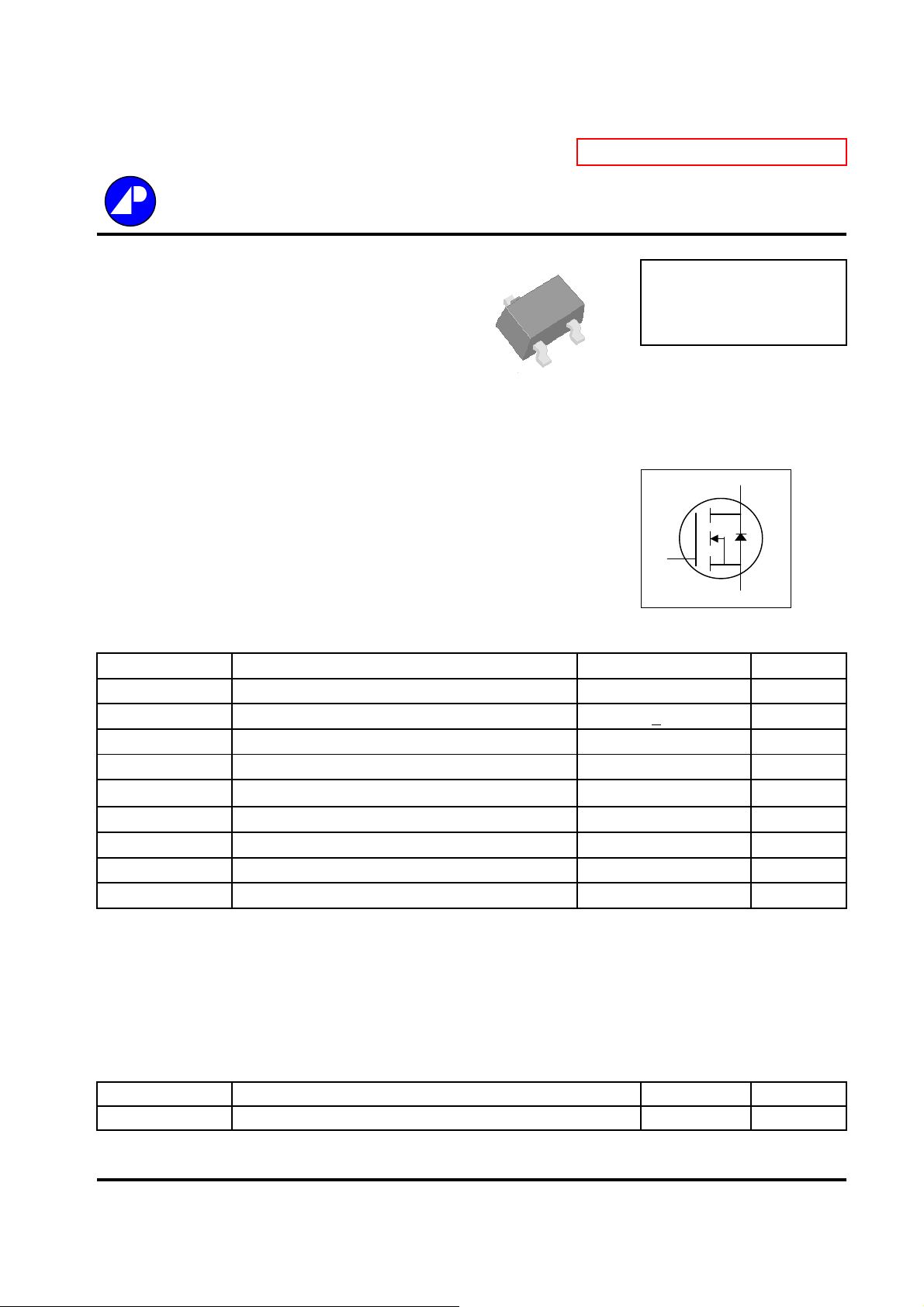
D
▼ Small Package Outline R
▼ Surface Mount Device I
▼ RoHS Compliant & Halogen-Free
SOT-23
S
G
BV
DS(ON)
D
DSS
Description
Advanced Power MOSFETs utilized advanced processing techniques to
achieve the lowest possible on-resistance, extremely efficient and
cost-effectiveness device.
The SOT-23 package is widely used for all commercial-industrial
applications.
G
Absolute Maximum Ratings
Symbol Units
V
DS
V
GS
=25℃ A
I
D@TA
=70℃ A
I
D@TA
I
DM
P
T
T
=25℃ W
D@TA
STG
J
Drain-Source Voltage 30
Gate-Source Voltage +
Continuous Drain Current
Continuous Drain Current
Pulsed Drain Current
Total Power Dissipation 1.38
Linear Derating Factor 0.01
Storage Temperature Range
Operating Junction Temperature Range -55 to 150
Parameter Rating
20
3
3
1
, VGS @ 10V
, VGS @ 10V
4.7
3.7
10
-55 to 150
30V
42mΩ
4.7A
D
S
V
V
A
W/℃
℃
℃
Thermal Data
Symbol Value Unit
Rthj-a Maximum Thermal Resistance, Junction-ambient
Data and specifications subject to change without notice
Parameter
3
90 ℃/W
1
201008182
AP2316GN-HF
Electrical Characteristics@Tj=25oC(unless otherwise specified)
Symbol Parameter Test Conditions Min. Typ. Max. Units
BV
ΔBV
R
DS(ON)
V
GS(th)
g
fs
I
DSS
I
GSS
Q
g
Q
gs
Q
gd
t
d(on)
t
r
t
d(off)
t
f
C
iss
C
oss
C
rss
R
g
DSS
DSS
/ΔT
Drain-Source Breakdown Voltage VGS=0V, ID=250uA 30 - - V
Breakdown Voltage Temperature Coefficient Reference to 25℃, I
j
=1mA - 0.02 - V/℃
D
Static Drain-Source On-Resistance VGS=10V, ID=4A - - 42 mΩ
=4.5V, ID=2A - - 72 mΩ
V
GS
Gate Threshold Voltage VDS=VGS, ID=250uA 1 - 3 V
Forward Transconductance VDS=10V, ID=4A - 5 - S
Drain-Source Leakage Current
Drain-Source Leakage Current (Tj=70oC)
=30V, VGS=0V - - 1
V
DS
VDS=24V ,VGS=0V - - 10
Gate-Source Leakage VGS=+20V - - +100
Total Gate Charge
2
ID=4A - 5 8
Gate-Source Charge VDS=24V - 1 Gate-Drain ("Miller") Charge VGS=4.5V - 3 Turn-on Delay Time
2
VDS=15V - 7 Rise Time ID=1A - 8 Turn-off Delay Time RG=3.3Ω,VGS=10V - 12 -
Fall Time RD=15Ω -3Input Capacitance VGS=0V - 270 430
Output Capacitance VDS=25V - 70 Reverse Transfer Capacitance f=1.0MHz - 60 Gate Resistance f=1.0MHz - 1.4 2.1
uA
uA
nA
nC
nC
nC
ns
ns
ns
ns
pF
pF
pF
Ω
Source-Drain Diode
Symbol Parameter Test Conditions Min. Typ. Max. Units
V
SD
t
rr
Q
rr
Forward On Voltage
Reverse Recovery Time
Reverse Recovery Charge dI/dt=100A/µs - 9 - nC
Notes:
1.Pulse width limited by Max. junction temperature.
2.Pulse width <
3.Surface mounted on 1 in
THIS PRODUCT IS SENSITIVE TO ELECTROSTATIC DISCHARGE, PLEASE HANDLE WITH CAUTION.
USE OF THIS PRODUCT AS A CRITICAL COMPONENT IN LIFE SUPPORT OR OTHER SIMILAR SYSTEMS IS NOT AUTHORIZED.
APEC DOES NOT ASSUME ANY LIABILITY ARISING OUT OF THE APPLICATION OR USE OF ANY PRODUCT OR CIRCUIT DESCRIBED
HEREIN; NEITHER DOES IT CONVEY ANY LICENSE UNDER ITS PATENT RIGHTS, NOR THE RIGHTS OF OTHERS.
APEC RESERVES THE RIGHT TO MAKE CHANGES WITHOUT FURTHER NOTICE TO ANY PRODUCTS HEREIN TO IMPROVE
RELIABILITY, FUNCTION OR DESIGN.
300us , duty cycle <2%.
2
copper pad of FR4 board , t <10sec ; 270 ℃/W when mounted on Min. copper pad.
2
2
IS=1.2A, VGS=0V - - 1.2 V
IS=4A, VGS=0V, - 14 -
ns
2

AP2316GN-HF
12
TA=25oC
10V
7.0V
5.0V
V
=3.0V
G
4.5V
8
, Drain Current (A)
4
D
I
0
01234
VDS , Drain-to-Source Voltage (V)
12
TA=150oC
10 V
7.0V
5.0V
V
=3.0V
G
4.5V
8
, Drain Current (A)
4
D
I
0
01234
VDS , Drain-to-Source Voltage (V)
Fig 1. Typical Output Characteristics Fig 2. Typical Output Characteristics
)
Ω
(m
DS(ON)
R
65
ID=2A
T
=25oC
A
55
45
35
DS(ON)
Normalized R
1.8
ID=4A
V
=10V
G
1.5
1.2
0.9
25
246810
VGS , Gate-to-Source Voltage (V)
0.6
-50 0 50 100 150
Tj , Junction Temperature (oC)
Fig 3. On-Resistance v.s. Gate Voltage Fig 4. Normalized On-Resistance
v.s. Junction Temperature
4.0
3.0
(A)
S
I
2.0
1.0
0.0
0 0.2 0.4 0.6 0.8 1 1.2
Tj=25oCTj=150oC
VSD , Source-to-Drain Voltage (V)
1.8
1.4
(V)
GS(th)
1.0
Normalized V
0.6
0.2
-50 0 50 100 150
Tj , Junction Temperature (oC)
Fig 5. Forward Characteristic of Fig 6. Gate Threshold Voltage v.s.
Reverse Diode Junction Temperature
3

AP2316GN-HF
f
z
10
1000
=1.0MH
ID=4A
8
=15V
V
DS
V
=20V
6
4
, Gate to Source Voltage ( V)
GS
V
2
0
02468
V
DS
=24V
DS
QG , Total Gate Charge (nC)
100
C (pF)
10
1 5 9 13 17 21 25 29
VDS , Drain-to-Source Voltage (V)
C
iss
C
oss
C
rss
Fig 7. Gate Charge Characteristics Fig 8. Typical Capacitance Characteristics
100
10
1
(A)
D
I
0.1
=25oC
T
A
Single Pulse
0.01
0.1 1 10 100
VDS , Drain-to-Source Voltage (V)
100us
1ms
10ms
100ms
1s
DC
1
Duty factor=0.5
)
thja
0.2
0.1
0.1
0.05
P
DM
0.01
0.01
Single Pulse
t
T
Duty factor = t/T
Peak T
= PDM x R
j
R
= 270℃/W
thja
Normalized Thermal Response (R
0.001
0.0001 0.001 0.01 0.1 1 10 100 1000
t , Pulse Width (s)
+ T
thja
a
Fig 9. Maximum Safe Operating Area Fig 10. Effective Transient Thermal Impedance
12
V
4.5V
G
Q
G
Q
GS
Q
GD
Charge
Q
=5V
V
DS
9
Tj=150oCTj=25oC
6
, Drain Current (A)
D
I
3
0
0246
VGS , Gate-to-Source Voltage (V)
Fig 11. Transfer Characteristics Fig 12. Gate Charge Circuit
4

 Loading...