Apec AP2307GN-HF-3 Schematic [ru]

Advanced Power
A
Electronics Corp.
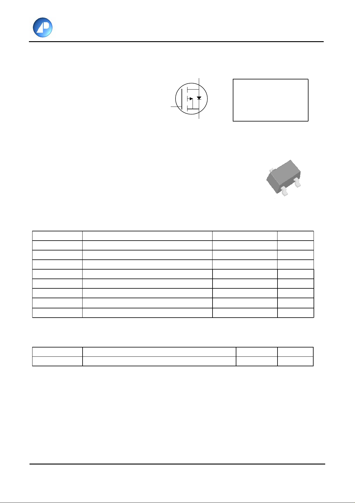
P-channel Enhancement-mode Power MOSFET
AP2307GN-HF-3
Simple Drive Requirement
Low On-resistance
Surface Mount Device R 60mΩ
G
RoHS-compliant, halogen-free I -4A
D
BV -16V
DSS
DS(ON)
S
D
Description
dvanced Power MOSFETs from APEC provide the designer with the best
combination of fast switching, low on-resistance and cost-effectiveness.
The AP2307GN-HF-3 is in the popular SOT-23 small surface-mount package
which is widely used in commercial and industrial applications where a small
board footprint is required.
This device is well suited for use in medium current applications such as
load switches and DC-DC converters.
SOT-23
D
G
Absolute Maximum Ratings
Symbol Units
V
DS
V
GS
at T =25°C -4 A
I Continuous Drain Current
D A
I
at T = 70°C -3.3 A
D A
I
DM
at TA=25°C
P Total Power Dissipation 1.38 W
D
T
STG
T Operating Junction Temperature Range -55 to 1
J
Drain-Source Voltage -16 V
Gate-Source Voltage
Continuous Drain Current
Pulsed Drain Current
Storage Temperature Range
Parameter Rating
±8 V
3
3
1
-12 A
-55 to 150 °C
50 °C
S
Thermal Data
Symbol Value Unit
Rthj-a Maximum Thermal Resistance, Junction-ambient
Parameter
90 °C/W
Ordering Information
AP2307GN-HF-3TR : RoHS-compliant halogen-free SOT-23, shipped on tape and reel, 3000pcs/ reel
©2011 Advanced Power Electronics Corp. USA 201003154-3
www.a-powerusa.com
1/5

Advanced Power
Electronics Corp.
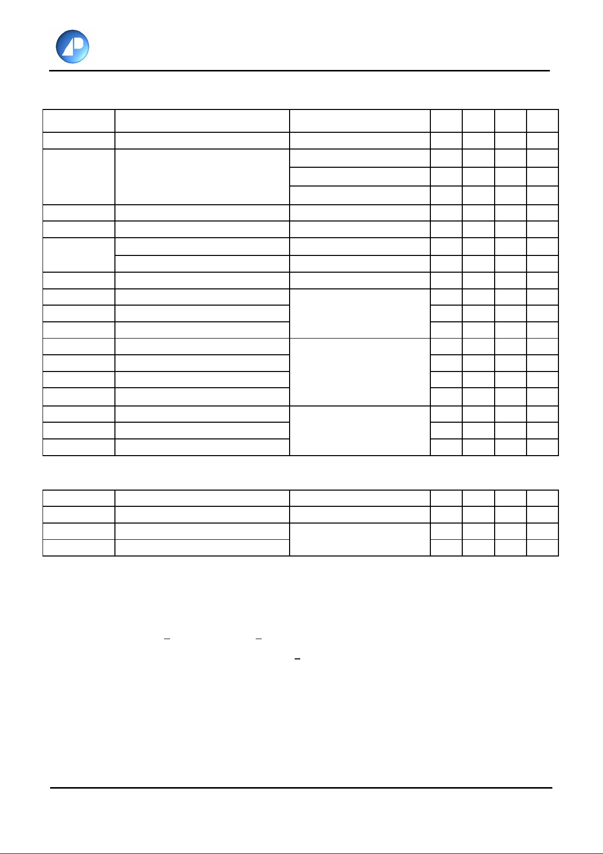
Electrical Specifications
at T
=25°C (unless otherwise specified)
j
AP2307GN-HF-3
Symbol Parameter Test Conditions
BV
DSS
R
DS(ON)
V
GS(th)
g
fs
I
DSS
I
GSS
Q
g
Q
gs
Q
gd
t
d(on)
t
r
t
d(off)
t
f
C
iss
C
oss
C
rss
Drain-Source Breakdown Voltage VGS=0V, ID=-250uA -16 - - V
V
=-4.5V, ID=-4A - - 60 mΩ
GS
Static Drain-Source On-Resistance
2
V
=-2.5V, ID=-3.0A - - 70 mΩ
GS
V
=-1.8V, ID=-2.0A - - 90 mΩ
GS
Gate Threshold Voltage VDS=VGS, ID=-250uA - - -1.0 V
Forward Transconductance VDS=-5V, ID=-4A - 12 - S
Drain-Source Leakage Current
Drain-Source Leakage Current (Tj=70oC)
V
=-16V, VGS=0V - - -1
DS
VDS=-12V, VGS=0V - - -25
Gate-Source Leakage VGS= ±8V, VDS=0V - - ±100
Total Gate Charge
2
ID=-4A - 15 24
Gate-Source Charge VDS=-12V - 1.3 Gate-Drain ("Miller") Charge VGS=-4.5V - 4 Turn-on Delay Time
2
VDS=-10V - 8 Rise Time ID=-1A - 11 Turn-off Delay Time RG=3.3Ω,VGS=-10V - 54 -
Fall Time RD=10Ω -36Input Capacitance VGS=0V - 985 1580
Output Capacitance VDS=-15V - 180 Reverse Transfer Capacitance f=1.0MHz - 160 -
Min. Typ. Max. Units
uA
uA
nA
nC
nC
nC
ns
ns
ns
ns
pF
pF
pF
Source-Drain Diode
Symbol Parameter Test Conditions Min. Typ. Max. Units
V
SD
t
rr
Q
rr
Forward On Voltage
Reverse Recovery Time
Reverse Recovery Charge dI/dt=100A/µs - 26 -
Notes:
1. Pulse width limited by maximum junction temperature.
2. Pulse test - pulse width < 300µs , duty cycle < 2%
2
3. Surface mounted on 1in
THIS PRODUCT IS SENSITIVE TO ELECTROSTATIC DISCHARGE, PLEASE HANDLE WITH CAUTION.
USE OF THIS PRODUCT AS A CRITICAL COMPONENT IN LIFE SUPPORT OR OTHER SIMILAR SYSTEMS IS NOT AUTHORIZED.
APEC DOES NOT ASSUME ANY LIABILITY ARISING OUT OF THE APPLICATION OR USE OF ANY PRODUCT OR CIRCUIT DESCRIBED
HEREIN; NEITHER DOES IT CONVEY ANY LICENSE UNDER ITS PATENT RIGHTS, NOR THE RIGHTS OF OTHERS.
APEC RESERVES THE RIGHT TO MAKE CHANGES WITHOUT FURTHER NOTICE TO ANY PRODUCTS HEREIN TO IMPROVE
RELIABILITY, FUNCTION OR DESIGN.
copper pad of FR4 board, t <10sec; 270°C/W when mounted on minimum copper pad.
2
2
IS=-1.2A, VGS=0V - - -1.2 V
IS=-4A, VGS=0V, - 39 -
ns
nC
©2011 Advanced Power Electronics Corp. USA
www.a-powerusa.com
2/5
 Loading...