

Page 1

Chapter 2
Hardware Installation
This chapter gives you a step-by-step procedure on how to install your system.
Follow each section accordingly.
Caution: Electrostatic discharge (ESD) can
damage your processor, disk drives, expansion
boards, and other components. Always
observe the following precautions before you
install a system component.
1. Do not remove a component from its
protective packaging until you are ready
to install it.
2. Wear a wrist ground strap and attach it to
a metal part of the system unit before
handling a component. If a wrist strap is
not available, maintain contact with the
system unit throughout any procedure
requiring ESD protection.
2-1
Page 2
Hardware Installation
COM1
PRINTER
JP14
VGA
JP28
JP23
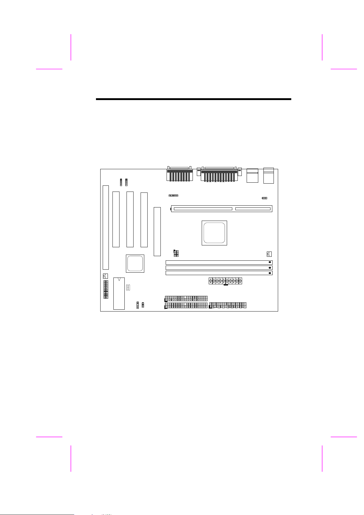
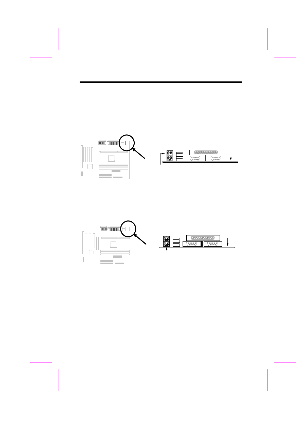
2.1 Jumper and Connector Locations
The following figure shows the locations of the jumpers and connectors on the
system board:
MODEM-CN CD-IN
USB
I
S
A
1
PANEL
FAN1
P
C
I
3
BIOS
WOL
WOM
P
P
C
C
I
I
2
1
A
G
P
IDE2
IDE1
IrDA
DIMM1
DIMM2
DIMM3
PWR2
FDC
KB2
PS/2 MS
CPUFAN1
2-2
Page 3

Hardware Installation
Jumpers:
JP14: Clear CMOS
JP23: AGP Ratio
JP28: Enable/Disable KB/MS Wake Up
Connectors:
PS2: PS/2 mouse connector
KB: PS/2 keyboard connector
COM1: COM1 connector
COM2: COM2 connector
PRINTER: Printer connector
PWR2: ATX power connector
USB: USB connector
FDC: Floppy drive connector
IDE1: IDE1 primary channel
IDE2: IDE2 secondary channel
CPUFAN1: CPU fan connector
FAN1: Housing fan connector
IrDA: IrDA (Infrared) connector
PANEL: Front panel (Multifunction) connector
CD-IN: CD-audio connector
MODEM-CN: Mono in (Pin 1-2) and Mic out (Pin 3-4)
WOM: Wake On Modem connector
WOL: Wake On LAN connector
2-3
Page 4
Hardware Installation
2.2 Jumpers
With the help of Pentium II / Pentium III / Celeron VID signal and SMbus, this
motherboard is jumper-less design.
2.2.1 Selecting the CPU Frequency
Celeron PPGA VID signal and SMbus clock generator provide CPU voltage
auto-detection and allow user to set CPU frequency through CMOS setup, no
jumper or switch is needed. The correct CPU information is saved into
EEPROM, with these technologies, the disadvantages of Pentium base jumperless design are eliminated. There will be no worry of wrong CPU voltage
detection and no need to re-open the housing if CMOS battery loss.
The CPU frequency selection is set by going into:
BOIS Setup à Chipset Features Setup à CPU Clock Frequency
(The possible setting is 66.8, 75, 83.3, 100, 103, 112, 124/31, 124/41, 133/33,
133/44, , 138, 143, 148 and 153 MHz)
BOIS Setup à Chipset Features Setup à CPU Clock Ratio
(The possible setting is 1.5x, 2x, 2.5x, 3x, 3.5x, 4x, 4.5x, 5x, 5.5x, 6x, 6.5x, 7x,
7.5x, and 8x)
Core frequency = CPU Ratio * CPU FSB
Intel Pentium II
/Pentium III
Pentium II - 233 233MHz = 3.5x 66MHz
Pentium II - 266 266MHz = 4x 66MHz
Pentium II - 300 300MHz = 4.5x 66MHz
Pentium II - 333 333MHz = 5x 66MHz
Pentium II - 350 350MHz= 3.5x 100MHz
Pentium II - 400 400MHz= 4x 100MHz
Pentium II - 450 450MHz= 4.5x 100MHz
Pentium III - 450 450MHz = 4.5x 100MHz
Pentium III - 500 500MHz = 5x 100MHz
Pentium III - 550 550MHz = 5.5x 100MHz
CPU Core Frequency Ratio External Bus Clock
INTEL Celeron CPU Core Frequency Ratio External Bus Clock
2-4
Page 5
Hardware Installation
3
3
INTEL Celeron CPU Core Frequency Ratio External Bus Clock
Celeron 266 266MHz = 4x 66MHz
Celeron 300 300MHz = 4.5x 66MHz
Celeron 300A 300MHz = 4.5x 66MHz
Celeron 333 333MHz = 5x 66MHz
Celeron 366 366MHz = 5.5x 66MHz
Celeron 400 400MHz = 6x 66MHz
Celeron 433 433MHz = 6.5x 66MHz
Celeron 466 466MHz = 7x 66MHz
Warning: INTEL 440ZX/BX chipset supports a maximum of
100MHz FSB, the higher clock settings are for internal test only.
These settings exceed the specification of ZX/BX chipset,
which may cause serious system damage.
2.2.2 Setting the CPU Voltage
This motherboard supports Pentium II \ Pentium III \ Celeron VID function, the
CPU core voltage is automatically detected, the range is from 1.3V to 3.5V.
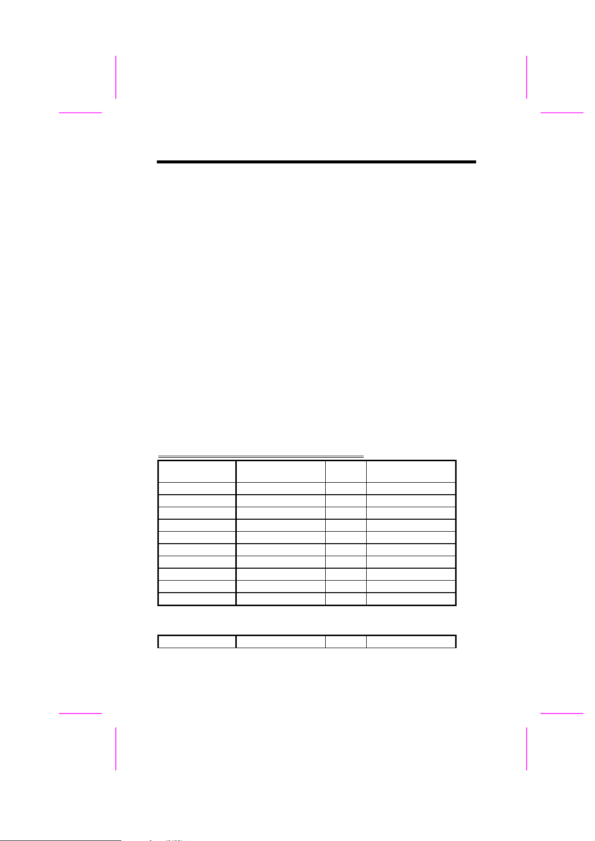
2.2.3 Clearing the CMOS
JP14
1-2
2-3
Clear CMOS
Normal operation
(default)
Clear CMOS
You need to clear the CMOS if you forget your
system password. To clear the CMOS, follow
the procedures as below:
JP14
1
2
Normal Operation
JP14
1
2
Clear CMOS
(default)
2-5
Page 6
Hardware Installation
1 2 3
The procedure to clear CMOS:
1. Turn off the system and unplug the AC power.
2. Remove ATX power cable from connector PWR2.
3. Locate JP14 and short pins 2-3 for a few seconds.
4. Return JP14 to its normal setting by shorting pins 1-2.
5. Connect ATX power cable back to connector PWR2.
6. Turn on the system power.
7. Press during bootup to enter the BIOS Setup Utility and specify a new
password, if needed.
Tip: If your system hangs or fails to boot because of over-clocking,
please clear CMOS and the system will go back to the default
setting (233MHz or 350MHz).
Tip: If your system hangs or fails to boot because of over-clocking,
simply use <Home> key to restore to the default setting. By this
smart design, it would be more convenient to clear CPU frequency
setting. For using this function, you just need to press <Home> key
first and then press Power button at the same time. Note that do
not release <Home> key until POST screen appearing.
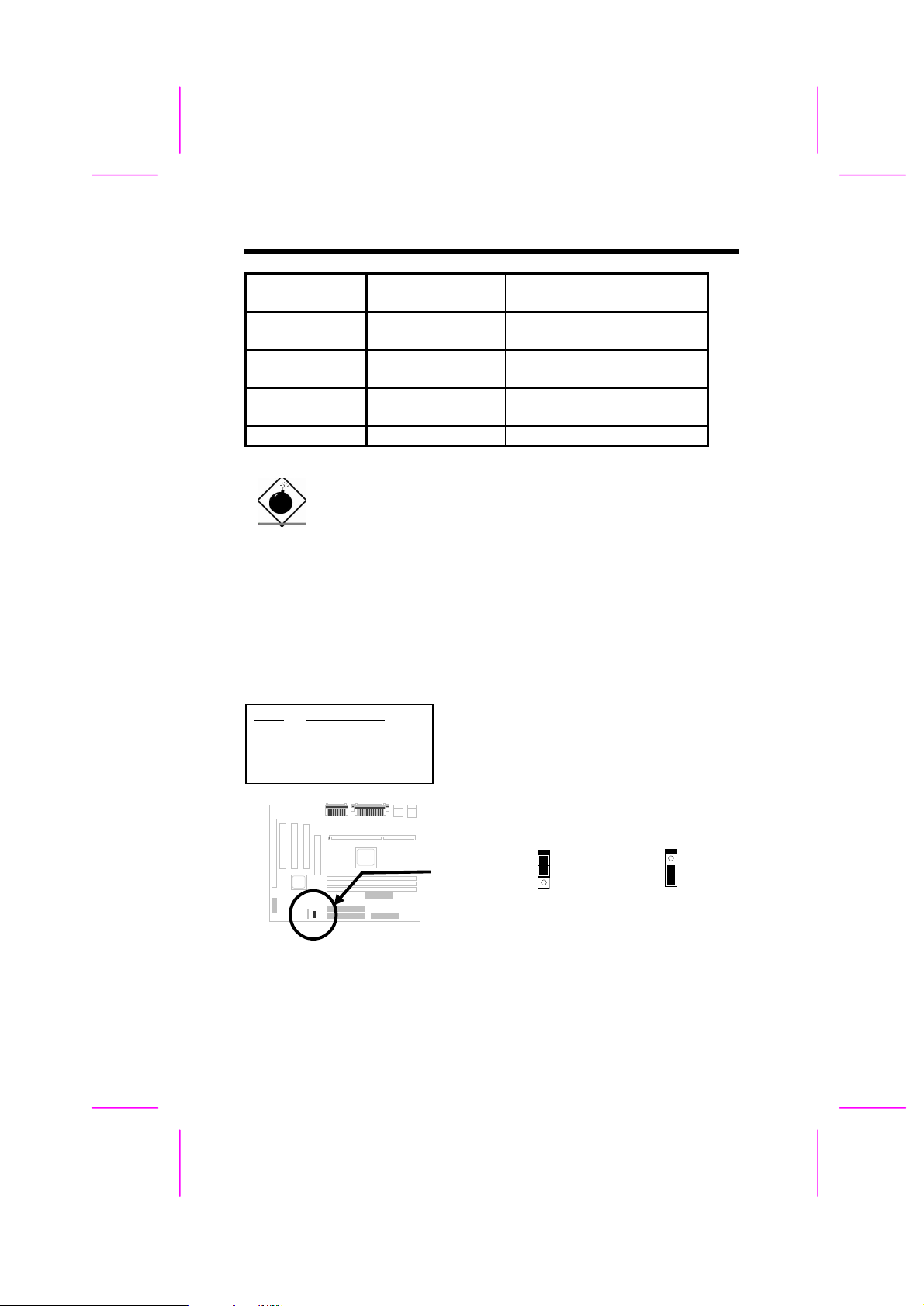
2.2.4 KB/MS Wakeup
JP28
1-2
2-3
2-6
KB/MS Wakeup
Disabled
Enabled
This jumper is used to enable or disable
Keyboard/Mouse Power ON function. If you
select Enabled, you may decide the wakeup
mode from BIOS Setup. To implement this
function, the 5V Stand By current must be
greater than 800mA.
Note that only PS/2 mouse supports Wake On
Mouse function.
JP28
1 2 3
Disabled
JP28
Enabled
Page 7

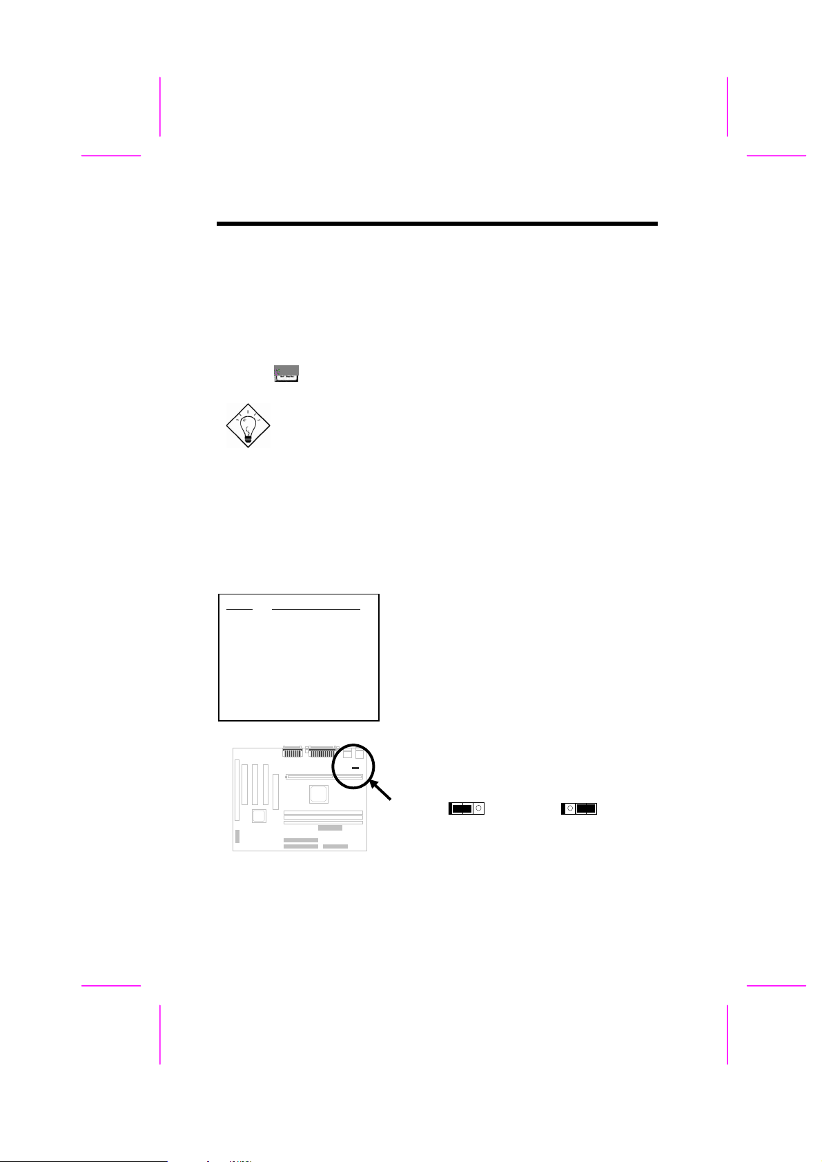
2.2.5 AGP Ratio
5
6
5
6
5
6
Hardware Installation
JP23
1-2
3-4
5-6
DC/Host Ratio
Auto (default)
2/3
1/1
To improve system performance, this motherboard
has implemented this jumper for setting the ratio of
the display cache and CPU external frequency.
JP23
1
3
JP23
2
4
1
3
JP23
2
4
1
2
3
4
Auto
2/3
1/1
(Default)
There is a "66/100" signal pin from CPU for ZX/BX chipset to automatically
identify AGP clock, this is important for jumperless design. When a 66MHz
Pentium II CPU is used, the north bridge will synchronize the CPU external
frequency and the AGP bus frequency. Therefore, when you set the CPU
external frequency to 100MHz, the AGP bus will also runs at 100MHz.
With 100MHz Pentium II CPU, the north bridge automatically set AGP frequency
to 2/3 AGP frequency. In other words, the AGP card will still runs at 66MHz while
the CPU is running at 100MHz external frequency.
Except Auto setting, you may also set this jumper to 2/3 or 1/1. Below is a table
for better understanding:
CPU Type 66/100 signal Bus clock AGP clock JP23
66MHz Low 66MHz 66MHz 1-2
66MHz Low 100MHz 100MHz 1-2
66MHz Low 100MHz 66MHz 3-4
100MHz High 100MHz 66MHz 1-2
100MHz High 100MHz 66MHz 3-4
100MHz High 100MHz 100MHz 5-6
100MHz High 133MHz 88.6MHz 1-2
100MHz High 133MHz 88.6MHz 3-4
100MHz High 133MHz 133MHz 5-6
Warning: The specification of AGP has a maximum of
100Mhz clock. A higher setting may cause the system
damage.
2-7
Page 8

Hardware Installation
5V SB
GND
2.3 Connectors
2.3.1 Power Cable
The ATX power supply uses 20-pin connector shown below. Make sure you
plug in the right direction.
Caution: Make sure that the power supply is off
before connecting or disconnecting the power cable.
+5V
3.3V
3.3V
+5V
PWR2
2.3.2 Fan
Plug in the fan cable to the 3-pin fan connector onboard. The fan connector is
marked CPUFAN1 and FAN1 on the system board.
+12V
SENSE
CPUFAN1
FAN1
2-8
Page 9
Hardware Installation
PS/2 Mouse
PS/2 KB
2.3.3 PS/2 Mouse
The onboard PS/2 mouse connector is a 6-pin Mini-Din connector marked
PS2. The view angle of drawing shown here is from back panel of the
housing.
PCB
2.3.4 Keyboard
The onboard PS/2 keyboard connector is a 6-pin Mini-Din connector marked
KB2. The view angle of drawing shown here is from back panel of the
housing.
PCB
2-9
Page 10

Hardware Installation
COM1
COM2
PRINTER
2.3.5 Serial Devices
The onboard serial connectors COM1 and COM2 are 9-pin D-type connectors
on the back panel of mainboard.
PCB
2.3.6 Printer
The onboard printer connector is a 25-pin D-type connector marked PRINTER.
The view angle of drawing shown here is from back panel of the housing.
2-10
PCB
Page 11

Hardware Installation
USB
34
33
2.3.7 USB Device
You can attach USB devices to the USB connector. The motherboard
contains two USB connectors, which are marked as USB.
PCB
2.3.8 Floppy Drive
Connect the 34-pin floppy drive cable to the floppy drive connector marked as
FDC on the system board.
2
1
FDC
2.3.9 IDE Hard Disk and CD ROM
This mainboard supports two 40 pin IDE connectors marked as IDE1 and
IDE2. IDE1 is also known as primary channel and IDE2 as secondary channel,
each channel supports two IDE devices that make total of four devices.
In order to work together, the two devices on each channel must be set
differently to master and slave mode, either one can be hard disk or CDROM.
The setting as master or slave mode depends on the jumper on your IDE
device, please refer to your hard disk and CDROM manual accordingly.
Connect your first IDE hard disk to master mode of the primary channel. If you
have second IDE device to install in your system, connect it as slave mode on
2-11
Page 12

Hardware Installation
1
40
2
39
1
40
2
39
(1st)
(2nd)
the same channel, and the third and fourth device can be connected on
secondary channel as master and slave mode respectively.
IDE2
IDE1
Caution: The specification of IDE cable is
maximum 46cm (18 inches), make sure your
cable does not excess this length.
Caution: For better signal quality, it is
recommended to set far end side device to
master mode and follow the suggested
sequence to install your new device. Please
refer to the following figure.
IDE1 (Primary Channel)
2-12
Slave
IDE2 (Second Channel)
Slave
(4th)
Master
Master
(3rd)
Page 13
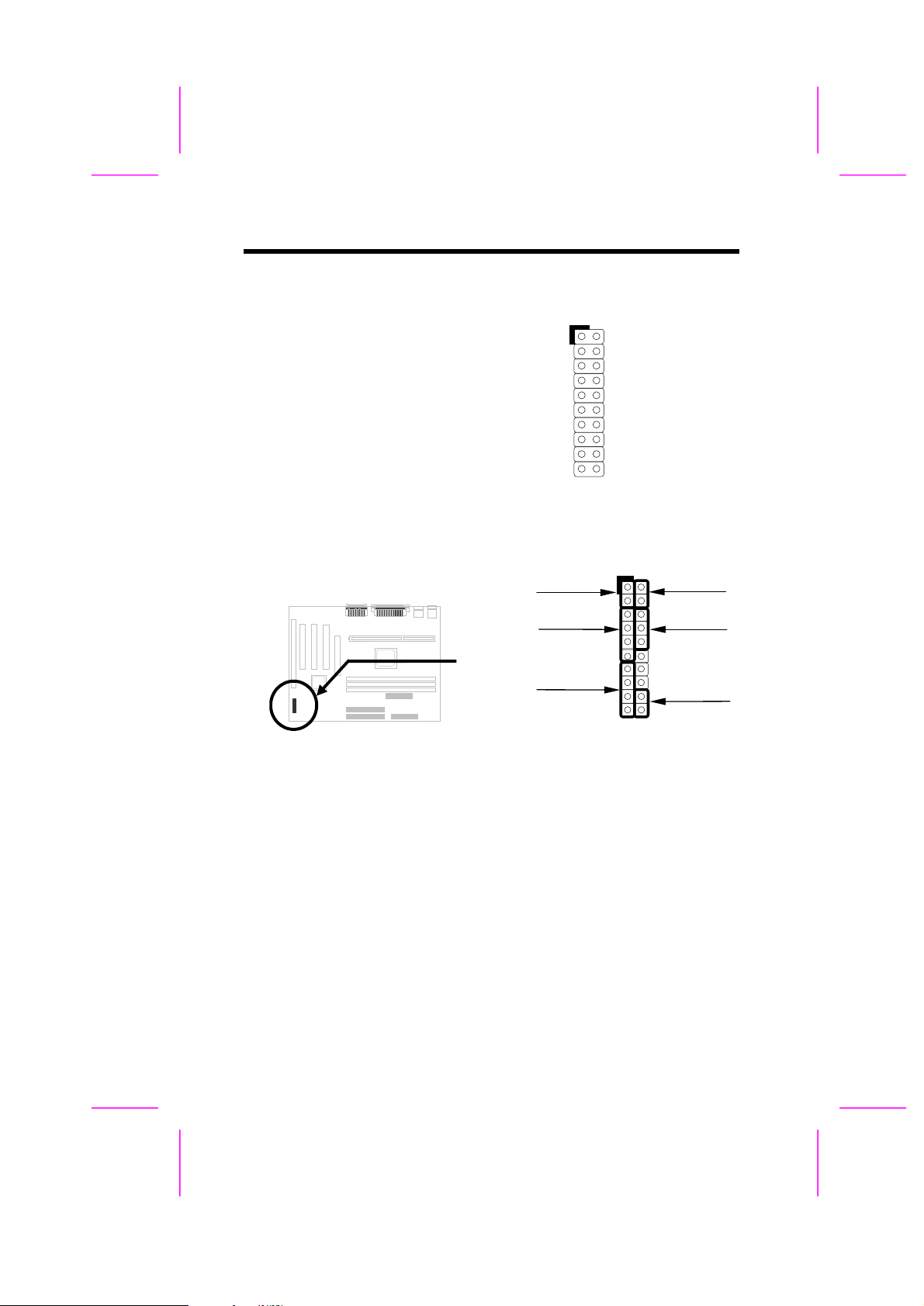
2.3.10 Panel Connector
1
11
10
20
+++
+
+
+
Hardware Installation
The Panel (multifunction) connector is
a 20-pin connector marked as PANEL
on the board. Attach the power LED,
keylock, speaker, SPWR, IDE LED
and reset switch to the corresponding
pins as shown in the figure.
If your ATX housing supports ACPI
specification, the ACPI & Power LED
will keep flashing if you have enabled
“suspend mode” item in the BIOS
Setup.
1
11
GND
KEYLOCK
+5V
IDE LED
IDE LED
+5V
+5V
GND
NC
SPEAKER
10 20
PANEL
Keylock
IDE LED
Speaker
PANEL
SPWR
GND
ACPI & POWER LED
GND
+5V
NC
NC
GND
RESET
GND
SPWR
ACPI &
Power LED
Reset
2-13
Page 14

Hardware Installation
1
2
3
4
5
6
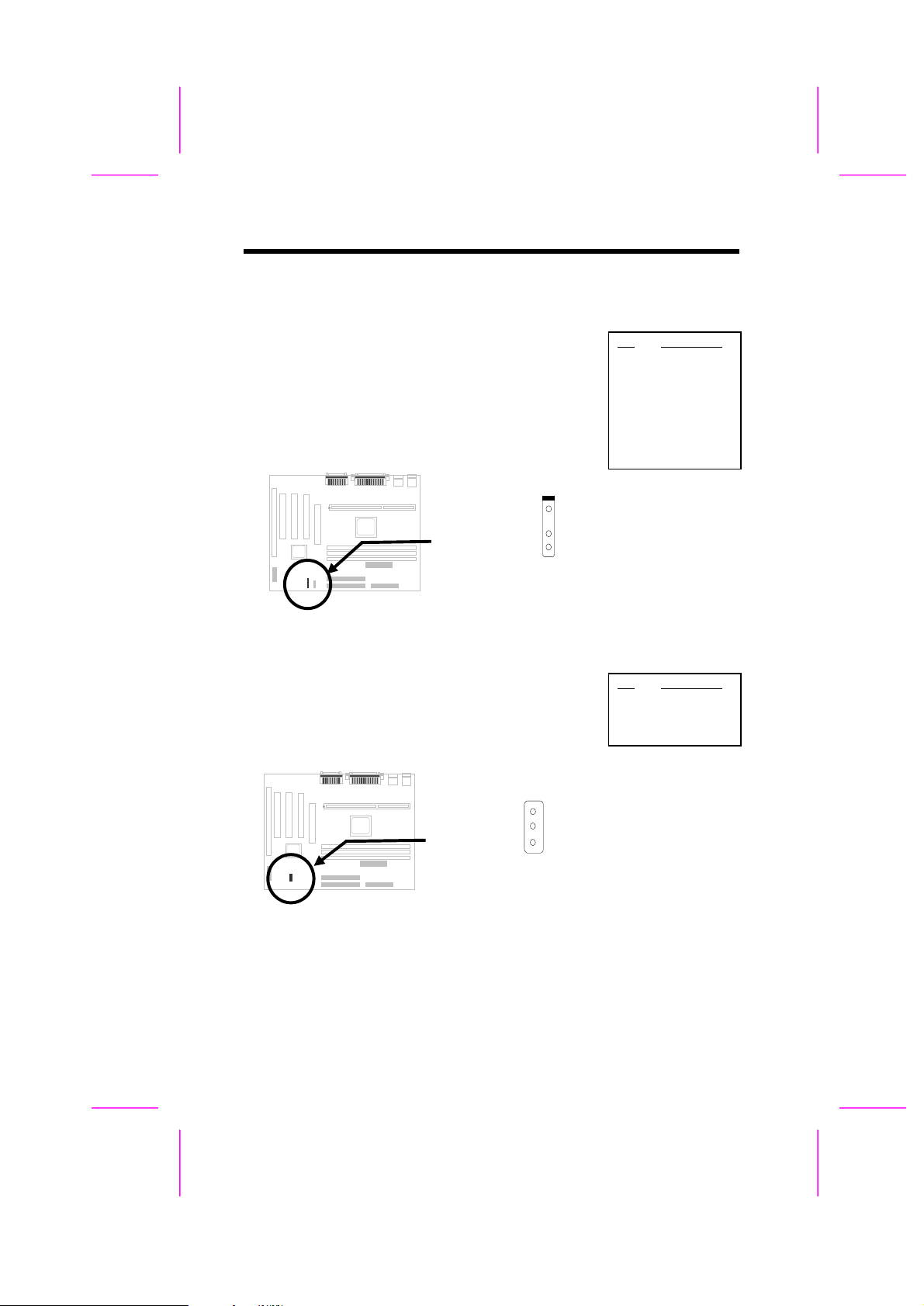
2.3.11 IrDA Connector
The IrDA connector can be configured to support wireless infrared module,
with this module and application software such as Laplink or Win95 Direct
Cable Connection, the user can transfer files to or from laptops, notebooks,
PDA devices and printers. This connector supports HPSIR (115.2Kbps, 2
meters) and ASK-IR (56Kbps).
Install the infrared module onto the IrDA
connector and enable the infrared
function from the BIOS setup, make sure
to have the correct orientation when you
plug in the IrDA connector.
Pin
1
2
3
4
5
6
Description
+5V
NC
IRRX
GND
IRTX
NC
IrDA
2-14
Page 15
Hardware Installation
2.3.12 Wake On Modem Connector
This motherboard implements special circuit to support
Wake On Modem, both Internal Modem Card (AOpen
MP56) and external box Modem are supported. Since
Internal Modem card consumes no power when system
power is off, it is recommended to use Internal Modem.
To use AOpen MP56, connect 4-pin cable from RING
connector of MP56 to WOM connector on the
mainboard.
1
2
3
4
WOM
2.3.13 Wake On LAN Connector
This mainboard implements a WOL connector. To use
Wake On LAN function, you need a network card that
supports this feature. In addition, you also need to
install a network management software.
Pin
1
2
3
4
Pin
1
2
3
Description
+5V SB
NC
RING
GND
Description
+5V SB
GND
LID
1
2
3
WOL
2-15
Page 16

Hardware Installation
2.3.14 CD Audio Connector
This connector is used to connect CD audio cable.
1
2
3
4
CD-IN
2.3.15 Mono In/Mic Out Connector
This connector is used to connect Mono In/Mic Out
connector of an internal modem card. The pin 1-2 is
Mono In, and the pin 3-4 is Mic Out. Please note
that there is no standard for this kind of connector
yet, only some internal modem cards implement this
connector.
Please see the pin definitions to connect the cable.
Pin
1
2
3
4
Pin
1
2
3
4
Description
L
GND
GND
R
Description
Mono In
GND
GND
Mic Out
2-16
1
2
3
4
MODEM-CN
Page 17

Hardware Installation
SPK
MIC
LINE-IN
Tape Deck,
Speakers
Microphone
Headphones
CD Player
2.3.16 Audio Connector
This motherboard comes with an onboard 16-bit audio processor (ESS Solo-1).
Game Port
PCB
To fully utilize the audio functions, you may connect various peripheral devices
that the audio chip supports. The following figure shows the different devices
that you can connect.
Stereo
Amplifier
SPK
Line-in
Mic
Synthesizer,
etc.
The audio drivers and applications are included in the AOpen Bonus Pack CD
disc.
2-17
Page 18

Hardware Installation
168
2.4 Configuring the System Memory
The DIMM types supported are
SDRAM (Synchronous DRAM) only.
This motherboard has three 168 pin
DIMM sockets (Dual-in-line Memory
Module) that allow you to install system
PIN1
Warning: This motherboard does not support Registered
SDRAMs and EDO DRAMs.
Warning: If you install two double-side SDRAMs, the possible
combinations are DIMM1&DIMM2 or DIMM1&DIMM3.
Warning: The maximum of 512MB can be implemented by
installing two 256MB SDRAM modules.
memory up to 512MB.
In case you install SDRAMs on
DIMM2 and DIMM3 at the same time,
it is crucial to identify single/double
side. For this configuration, only
single-side SDRAMs are acceptable.
I. Size: single side, 1Mx64 (8MB), 2Mx64 (16MB), 4Mx64 (32MB), 8Mx64
(64MB), 16Mx64 (128MB), and double side, 1Mx64x2 (16MB), 2Mx64x2
(32MB), 4Mx64x2 (64MB), 8Mx64x2 (128MB).
Tip: Here is a trick to check if your DIMM is single-side or
double-side -- if there are traces connected to golden finger
pin 114 and pin 129 of the DIMM, the DIMM is probably
double-side; otherwise, it is single-side. The following figure
is for your reference.
Pin 129
2-18
Pin 114
Page 19

Hardware Installation
II. Speed: Normally marked as -12, which means the clock cycle time is 12ns
and the maximum clock of this SDRAM is 83MHz. Sometimes you can also
find the SDRAM marked as -67, which means maximum clock is 67MHz.
Caution: Some SDRAMs marked as -10 may
work fine with 100 MHz CPU clock, but not all
of these kinds of modules can work properly
under 100MHz external clock. We suggest you
choose and install SDRAMs that match PC 100
specification if 100MHz or above CPU clock is
selected.
III. Buffered and non-buffered: This motherboard supports non-buffered
DIMMs only. You can identify non-buffered DIMMs and buffered DIMMs
according to the position of the notch. The following figure is for your
reference:
Reserved
non-buffered
buffered
Because the positions are different, only non-buffered DIMMs can be inserted
into the DIMM sockets on this motherboard. Although most DIMMs available in
the current market are non-buffered, we still recommend you ask your dealer
for the correct type.
IV. 2-clock and 4-clock signals: Although both 2-clock and 4-clock signals
are supported by this motherboard, we strongly recommend choosing 4clock SDRAM for its reliability.
Tip: To identify 2-clock and 4-clock SDRAM, you
may check if there are traces connected to the
golden finger pins 79 and 163 of the SDRAM. If
there are traces, the SDRAM is probably 4-clock;
Otherwise, it is 2-clock.
V. Parity: This motherboard supports standard 64 bit wide (without parity)
DIMM modules.
VI. SPD support: The BIOS will automatically detect DIMMs with SPD, and set
to the appropriate timing. DIMMs without SPD are still able to work fine on
this board, but the BIOS POST screen will give you a warning message that
you use a DIMM without SPD.
2-19
Page 20

Hardware Installation
There is no jumper setting required for the memory size or type. It is
automatically detected by the system BIOS, and the total memory size is all of
them added together.
Total Memory Size = Size of DIMM1 + Size of DIMM2 + Size of DIMM3
The following table lists the recommended SDRAM combinations of DIMM:
DIMM
Data chip
1M by 16 1Mx64 x1 4 8MB Yes
1M by 16 1Mx64 x2 8 16MB Yes
2M by 8 2Mx64 x1 8 16MB Yes
2M by 8 2Mx64 x2 16 32MB Yes
4M by 16 4Mx64 x1 4 32MB Yes
4M by 16 4Mx64 x2 8 64MB Yes
8M by 8 8Mx64 x1 8 64MB Yes.
8M by 8 8Mx64 x2 16 128MB Yes.
DIMM
Data chip
2M by 32 2Mx64 x1 2 16MB Yes, but not tested.
2M by 32 2Mx64 x2 4 32MB Yes, but not tested.
Bit size
per side
Bit size
per side
Single/
Double side
Single/
Double side
Chip
count
Chip
count
DIMM size Recommended
DIMM size Recommended
The following table lists possible SDRAM combinations that is NOT
recommended:
DIMM
Data chip
4M by 4 4Mx64 x1 16 32MB No
4M by 4 4Mx64 x2 32 64MB No
16M by 4 16Mx64 x1 16 128MB No
Bit size
per side
Single/
Double side
Chip
count
DIMM size Recommended
2-20
 Loading...