

Page 1

l
l
MMXX4466LLSS--VV // MMXX4466LLSS--553333VV OOnnlliinnee MMaannuua
MX46LS-V / MX46LS-533V
DOC. NO.: MX46LSV-OL-E0301B
a
Overview
Installation
Hardware
Drivers &
Utilities
BIOS Setup
AWARD
Glossary
Troubleshooting &
Technical Support
1
Page 2

l
l
MMXX4466LLSS--VV // MMXX4466LLSS--553333VV OOnnlliinnee MMaannuua
a
WWhhaatt’’ss iinn tthhiiss mmaannuuaall
MX46LS-V / MX46LS-533V............................................................................................................................. 1
What’s in this manual................................................................................................................................................................ 2
You Must Notice........................................................................................................................................................................ 8
Before You Start........................................................................................................................................................................9
Overview................................................................................................................................................................................. 10
Feature Highlight .....................................................................................................................................................................11
Quick Installation Procedure ................................................................................................................................................... 15
Motherboard Map ................................................................................................................................................................... 16
Block Diagram ........................................................................................................................................................................ 17
Hardware Installation ............................................................................................................................18
About “User Upgrade Optional” and “Manufacture Upgrade Optional”… ................................................................................. 19
CPU Installation ...................................................................................................................................................................... 20
Enlarged Aluminum Heatsink.................................................................................................................................................. 23
Full-range Adjustable CPU Core Voltage................................................................................................................................. 24
CPU and System Fan Connectors (with H/W Monitoring) ..................................................................................................... 26
DIMM Sockets ........................................................................................................................................................................ 27
Front Panel Connector............................................................................................................................................................ 29
ATX Power Connector............................................................................................................................................................. 30
2
Page 3

l
l
MMXX4466LLSS--VV // MMXX4466LLSS--553333VV OOnnlliinnee MMaannuua
AC Power Auto Recovery........................................................................................................................................................ 30
IDE and Floppy Connector...................................................................................................................................................... 31
ATA133 Supported.................................................................................................................................................................. 33
IrDA Connector....................................................................................................................................................................... 34
AGP (Accelerated Graphic Port) Expansion Slot..................................................................................................................... 35
WOL (Wake on LAN) .............................................................................................................................................................. 36
Support 10/100 Mbps LAN onboard ........................................................................................................................................ 38
CNR (Communication and Network Riser) Expansion Slot...................................................................................................... 39
Support Three USB2.0 Channels (Six Ports)........................................................................................................................... 40
Color Coded Back Panel......................................................................................................................................................... 41
Chassis Intrusion Connector................................................................................................................................................... 42
CD Audio Connector............................................................................................................................................................... 43
MODEM-IN Connector............................................................................................................................................................ 44
COM2 Connector.................................................................................................................................................................... 45
Front Audio Connector............................................................................................................................................................ 46
S/PDIF (Sony/Philips Digital Interface) Connector................................................................................................................... 47
JP14 Clear CMOS Data.......................................................................................................................................................... 48
JP28 USB Keyboard/Mouse Wake-up Enable/Disable Jumper ............................................................................................... 49
Battery-less and Long Life Design .......................................................................................................................................... 51
a
3
Page 4

l
l
MMXX4466LLSS--VV // MMXX4466LLSS--553333VV OOnnlliinnee MMaannuua
Over-current Protection........................................................................................................................................................... 52
Resetable Fuse....................................................................................................................................................................... 53
Low ESR Capacitor................................................................................................................................................................. 54
Phoenix-AWARD BIOS ............................................................................................................................56
About BIOS Function Description… ........................................................................................................................................ 57
How To Use Phoenix-Award™ BIOS Setup Program .............................................................................................................. 58
How To Enter BIOS Setup....................................................................................................................................................... 60
BIOS Upgrade under Windows environment ........................................................................................................................... 61
Driver and Utility.................................................................................................................................... 63
Auto-run Menu from Bonus CD............................................................................................................................................... 63
Install IDE Driver..................................................................................................................................................................... 64
Installing AGP Driver............................................................................................................................................................... 65
Installing VGA Driver............................................................................................................................................................... 66
Install USB2.0 Driver............................................................................................................................................................... 67
Installing LAN Driver ............................................................................................................................................................... 68
Installing Onboard Sound Driver ............................................................................................................................................. 69
AOConfig Utility ...................................................................................................................................................................... 70
Installing Hardware Monitoring Utility ...................................................................................................................................... 72
Glossary .................................................................................................................................................73
a
4
Page 5

l
l
MMXX4466LLSS--VV // MMXX4466LLSS--553333VV OOnnlliinnee MMaannuua
AC97 CODEC......................................................................................................................................................................... 73
ACPI (Advanced Configuration & Power Interface) ................................................................................................................. 73
ACR (Advanced Communication Riser) .................................................................................................................................. 73
AGP (Accelerated Graphic Port) ............................................................................................................................................. 74
AMR (Audio/Modem Riser) ..................................................................................................................................................... 74
ATA (AT Attachment)............................................................................................................................................................... 74
BIOS (Basic Input/Output System).......................................................................................................................................... 75
Bluetooth ................................................................................................................................................................................ 75
CNR (Communication and Networking Riser) ......................................................................................................................... 76
DDR (Double Data Rate) RAM................................................................................................................................................ 76
ECC (Error Checking and Correction)..................................................................................................................................... 76
EEPROM (Electronic Erasable Programmable ROM) ............................................................................................................. 77
EPROM (Erasable Programmable ROM)................................................................................................................................ 77
EV6 Bus.................................................................................................................................................................................. 77
FCC DoC (Declaration of Conformity) ..................................................................................................................................... 77
FC-PGA (Flip Chip-Pin Grid Array).......................................................................................................................................... 78
FC-PGA2 (Flip Chip-Pin Grid Array)........................................................................................................................................ 78
Flash ROM ............................................................................................................................................................................. 78
Hyper Threading..................................................................................................................................................................... 78
a
5
Page 6

l
l
MMXX4466LLSS--VV // MMXX4466LLSS--553333VV OOnnlliinnee MMaannuua
IEEE 1394 .............................................................................................................................................................................. 79
Parity Bit................................................................................................................................................................................. 79
PCI (Peripheral Component Interface) Bus ............................................................................................................................. 80
PDF Format............................................................................................................................................................................ 80
PnP (Plug and Play)................................................................................................................................................................ 80
POST (Power-On Self Test) .................................................................................................................................................... 80
PSB (Processor System Bus) Clock........................................................................................................................................ 81
RDRAM (Rambus Dynamic Random Access Memory) ........................................................................................................... 81
RIMM (Rambus Inline Memory Module).................................................................................................................................. 81
SDRAM (Synchronous DRAM) ............................................................................................................................................... 81
SATA (Serial ATA) ................................................................................................................................................................... 82
SMBus (System Management Bus) ........................................................................................................................................ 82
SPD (Serial Presence Detect)................................................................................................................................................. 82
USB 2.0 (Universal Serial Bus) ............................................................................................................................................... 82
VCM (Virtual Channel Memory) .............................................................................................................................................. 83
Wireless LAN – 802.11b.......................................................................................................................................................... 83
ZIP file .................................................................................................................................................................................... 83
Troubleshooting .....................................................................................................................................84
Technical Support ..................................................................................................................................88
a
6
Page 7

l
l
MMXX4466LLSS--VV // MMXX4466LLSS--553333VV OOnnlliinnee MMaannuua
Product Registration.............................................................................................................................. 91
How to Contact Us................................................................................................................................. 92
a
7
Page 8

l
l
MMXX4466LLSS--VV // MMXX4466LLSS--553333VV OOnnlliinnee MMaannuua
a
YYoouu MMuusstt NNoottiiccee
Adobe, the Adobe logo, Acrobat is trademarks of Adobe Systems Incorporated.
AMD, the AMD logo, Athlon and Duron are trademarks of Advanced Micro Devices, Inc.
Intel, the Intel logo, Intel Celeron, Pentium II, Pentium III and Pentium 4 are trademarks of Intel Corporation.
Microsoft, Windows, and Windows logo are either registered trademarks or trademarks of Microsoft Corporation in the United States and/or
other countries.
All product and brand names used on this manual are used for identification purposes only and may be the registered trademarks of their
respective owners.
All of the specifications and information contained in this manual are subject to change without notice. AOpen reserves the right to revise
this publication and to make reasonable changes. AOpen assumes no responsibility for any errors or inaccuracies that may appear in this
manual, including the products and software described in it.
This documentation is protected by copyright law. All rights are reserved.
No part of this document may be used or reproduced in any form or by any means, or stored in a database or retrieval system
without prior written permission from AOpen Corporation.
Copyright
©
1996-2003, AOpen Inc. All Rights Reserved.
8
Page 9

l
l
MMXX4466LLSS--VV // MMXX4466LLSS--553333VV OOnnlliinnee MMaannuua
a
BBeeffoorree YYoouu SSttaarrtt
This Online Manual will introduce to the user how this product is installed. All useful information will be described in later chapters. Please
keep this manual carefully for future upgrades or system configuration changes. This Online Manual is saved in PDF format
recommend using Adobe Acrobat Reader 4.0 for online viewing, it is included in Bonus CD
site.
Although this Online Manual is optimized for screen viewing, it is still capable for hardcopy printing, you can print it by A4 paper size and set
2 pages per A4 sheet on your printer. To do so, choose File > Page Setup and follow the instruction of your printer driver.
Thanks for the help of saving our earth.
, we
or you can get free download from Adobe web
9
Page 10

l
l
MMXX4466LLSS--VV // MMXX4466LLSS--553333VV OOnnlliinnee MMaannuua
a
OOvveerrvviieeww
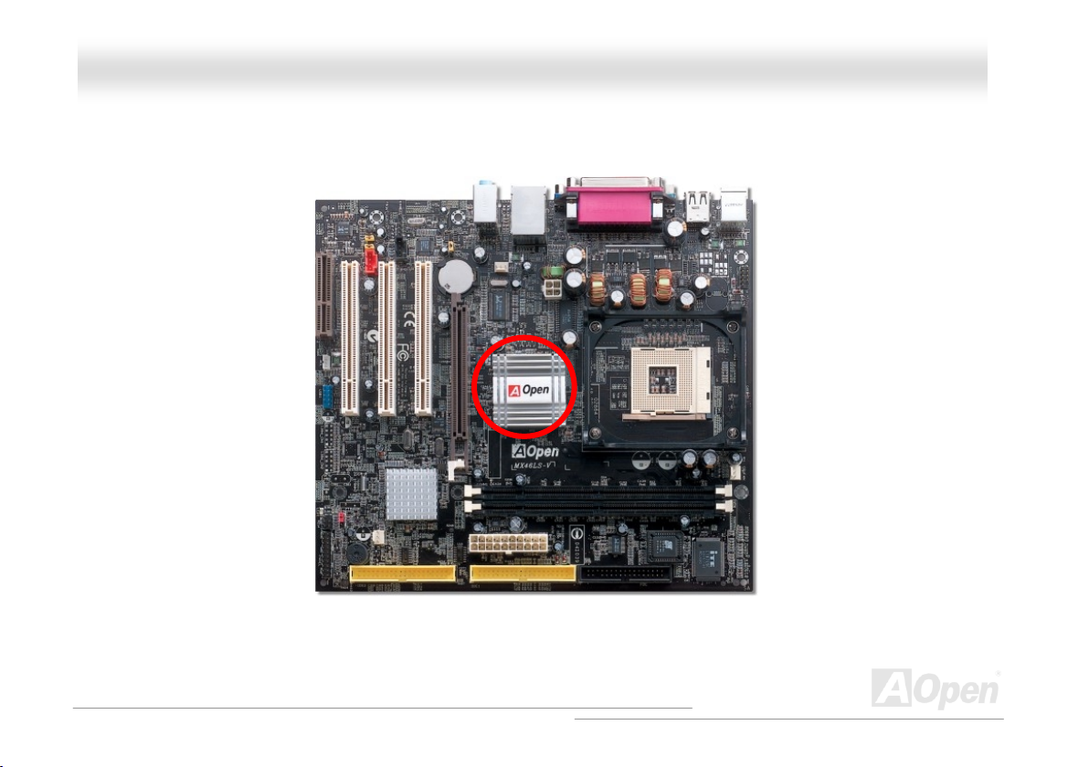
Thank you for choosing AOpen MX46LS-V / MX46LS-533V motherboard. MX46LS-V / MX46LS-533V is Intel® Socket 478 motherboard
(M/B) based on the micro-ATX form factor featuring the SIS 650GX chipset
chipset built in the M/B, MX46LS-V supports Intel
clock. MX46LS-533V supports Intel
the AGP performance, it has one AGP slot and supports AGP
According to different customer’s requirements, MX46LS-V / MX46LS-533V supports PC100/PC133 SDRAM up to 1GB maximum. The
onboard IDE controller supports Ultra DMA
Realtek PHY on board, which is a highly integrated Platform LAN Connect device, it provides 10/100M bps Ethernet for office and home
use. Six USB 2.0
chipset onboard providing high performance and magic surround stereo sound to let people enjoy working with
it. Now, let’s enjoy all features from AOpen MX46LS-V / MX46LS-533V motherboard.
®
®
Socket 478 Pentium® 4 (Willamette / Northwood) and 400MHz/533MHz Front Side Bus (FSB) clock. In
ports are supported with a fancy speed of up to 480Mbps. Besides, MX46LS-V / MX46LS-533V has an AC97 CODEC
Socket 478 Pentium® 4 (Willamette / Northwood) and 400MHz Front Side Bus (FSB)
4X mode and pipelined spilt-transaction long burst transfer up to 1056MB/sec.
33/66/100/133 mode. More than that, on the strength of integrated SiS LAN controller with
(MX46LS-V) and the SIS 651 chipset. As high performance
10
Page 11

l
l
MMXX4466LLSS--VV // MMXX4466LLSS--553333VV OOnnlliinnee MMaannuua
a
FFeeaattuurree HHiigghhlliigghhtt
CPU
MX46LS-V supports Intel® Socket 478 Pentium® 4 (Willamette / Northwood) 1.4GHz~2.8GHz+ with 400MHz Front Side Bus (FSB) designed
for Socket 478 technology and MX46LV-533V with 400MHz/533MHz Front Side Bus (FSB).
Chipset
MX46LS-V
This motherboard is equipped with SIS 650GX chipset. SiS 650GX chipset consists of host interface Controller and integrated high
performance SDRAM
with SiS 650GX, the SIS 962L chipset is integrated fast Ethernet/Home networking controller, Audio/Modem Controller with AC’97 interface
and advanced power management, which can strongly enhance the system performance.
MX46LS-533V
This motherboard is equipped with SIS 651 chipset. SIS 651 IGUI Host Memory Controller integrates a high performance host interface for
Intel Pentium 4 processor, a high performance 2D/3D Graphic Engine, a high performance memory controller and an AGP 4X interface.
SiS651 Host Interface features the AGTL & AGTL+ compliant bus driver technology with integrated on-die termination to support Intel
Pentium 4 series processors with FSB 100MHz and over clocking up to 133MHz. SiS651 also can support external AGP slot with AGP
1X/2X/4X capability and Fast Write Transactions.
The South Bridge SIS 962L MuTIOL Media I/O integrates one Universal Serial Bus 2.0 Host Controllers, the Audio Controller with AC97
Interface, three Universal Serial Bus 1.1 Host Controllers and the IDE Master/Slave controllers. The PCI to LPC bridge, I/O Advanced
Host system controller, which provides superior performance among CPU, SDRAM, and AGP buses. In coordination
11
Page 12

l
l
MMXX4466LLSS--VV // MMXX4466LLSS--553333VV OOnnlliinnee MMaannuua
Programmable Interrupt Controller, legacy system I/O and legacy power management functionalities are integrated as well. The SIS 961B
chipset integrated fast Ethernet/Home networking controller, Audio/Modem Controller with AC’97 interface and advanced power
management, which can strongly enhance the system performance.
a
Expansion Slots
Including three 32-bit/33MHz PCI, one AGP 1X/2X/4X slots. The PCI local bus throughput can be up to 132MB/s. The Accelerated Graphics
Port (AGP) specification provides a new level of video display sophistication and speed. The AGP video cards support data transfer rate up
to 1056MB/s. MX46LS-V / MX46LS-533V motherboard includes one AGP expansion slot for a bus mastering AGP graphic card. For AD
and SBA signaling, MX46LS-V / MX46LS-533V motherboard can support 4X mode. Of three PCI slots provided, all of them are master PCI
slots with arbitration and decoding for all integrated functions and LPC bus.
Memory
MX46LS-V / MX46LS-533V provides two 168-pin SDRAM SIMM sockets that support up to 1GB of PC100/PC133 compliant SDRAM
(Synchronous Dynamic Random Access Memory).
Watch Dog Timer
Includes AOpen “Watch Dog Timer” function that can auto-reset system in 4.8 seconds when you fail to system overclocking.
1MHz Stepping CPU Frequency Adjustment
Provides “1MHz Stepping CPU Frequency Adjustment” function in the BIOS. This magic function allows you to adjust CPU FSB frequency
from 100~248MHz by 1MHz stepping adjustment, and helps your system get maximum performance.
12
Page 13

l
l
MMXX4466LLSS--VV // MMXX4466LLSS--553333VV OOnnlliinnee MMaannuua
a
LAN Port
On the strength of integrated SiS LAN controller with Realtek PHY on board, which is a highly integrated Platform LAN Connect device, it
provides 10/100 Mbps Ethernet for office and home use.
Ultra DMA 33/66/100/133 Bus Mater IDE
Comes with an on-board PCI Bus Master IDE controller with two connectors that support four IDE devices in two channels, supports Ultra
DMA 33/66/100/133, PIO Modes 3 and 4 and Bus Master IDE DMA Mode 6, and supports Enhanced IDE devices.
On-board AC’97 Sound
MX46LS-V / MX46LS-533V uses RealTek AC97 sound chip. This on-board audio includes a complete audio recording and playback
system.
3 USB2.0 Channels (6 Ports)
Provides 3 USB2.0 channels (6 ports) for USB interface devices, such as mouse, keyboard, modem, scanner, etc.
S/PDIF Connectors
S/PDIF (Sony/Philips Digital Interface) is the newest audio transfer file format, which provides impressive quality through optical fiber and
allows you to enjoy digital audio instead of analog audio.
13
Page 14

l
l
MMXX4466LLSS--VV // MMXX4466LLSS--553333VV OOnnlliinnee MMaannuua
Power Management/Plug and Play
Supports the power management function that confirms to the power-saving standards of the U.S. Environmental Protection Agency (EPA)
Energy Star program. It also offers Plug-and-Play
user-friendlier.
Hardware Monitoring Management
Supports CPU or system fans status, temperature and voltage monitoring and alert, through the on-board hardware monitor module.
Enhanced ACPI
Fully implement the ACPI standard for Windows® 98/ME/2000 series compatibility, and supports Soft-Off, STR (Suspend to RAM, S3), STD
(Suspend to Disk, S4) features.
Super Multi-I/O
Provides two high-speed UART compatible serial ports and one parallel port with EPP and ECP capabilities. UART can also be directed
from COM1 to the Infrared Module for the wireless connections.
, which helps save users from configuration problems, thus making the system much
a
14
Page 15

l
l
MMXX4466LLSS--VV // MMXX4466LLSS--553333VV OOnnlliinnee MMaannuua
a
QQuuiicckk IInnssttaallllaattiioonn PPrroocceedduurree
This page gives you a quick procedure on how to install your system. Follow each step accordingly.
1. Installing CPU and Fan
2. Installing System Memory (DIMM)
3. Connecting Front Panel Cable
4. Connecting IDE and Floppy Cable
5. Connecting ATX Power Cable
6. Connecting Back Panel Cable
7. Power-on and Load BIOS Setup Default
8. Setting CPU Frequency
9. Reboot
10. Installing Operating System (such as Windows 98)
11. Installing Driver and Utility
15
Page 16
l
l
r
r
Y
r
r
r
r
r
A
r
A
A
r
r
r
r
r
r
A
r
t
MMXX4466LLSS--VV // MMXX4466LLSS--553333VV OOnnlliinnee MMaannuua
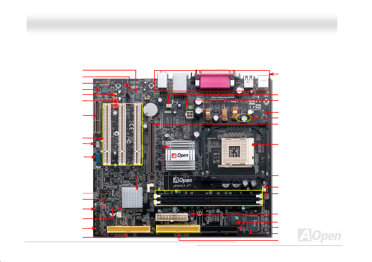
Motherboard Map
Realtek Ethernet PH
CD-IN Connecto
S/PDIF Connecto
AC’97 CODEC
Front Audio Connecto
MODEM-IN Connecto
CNR Slo
32-bit PCI Expansion Slot x3
WOL Connecto
rd
USB2.0 channels
3
SYSFAN2 Connecto
JP14 CMOS Clear Jumpe
TA 100/133 IDE1 Connecto
IrDA Connecto
Case Open Connecto
Front Panel Connecto
16
PC99 Colored Back Panel
SYSFAN3 Connecto
4-pin 12V. ATX Power Connector
COM2 Connecto
Low ESR Capacitors
GP 4x Expansion Slot
478-pin CPU socket (Willamette/
Northwood) with Voltage and
Frequency Auto-detection that
supports Intel
1.4~2.8GHz+ CPU
SIS 650GX/962L Chipset (MX46LS-V)
SIS 651/962L Chipset (MX46LS-533V)
CPUFAN1 connecto
168-pin SIMMx2 supports
PC100/133 SDRAM maximum
up to 1GB
TX Power Connector
Flash ROM BIOS
FDD Connector
ITE IT8705
TA 100/133 IDE2 Connecto
a
®
Pentium® 4
Page 17
l
l
MMXX4466LLSS--VV // MMXX4466LLSS--553333VV OOnnlliinnee MMaannuua
a
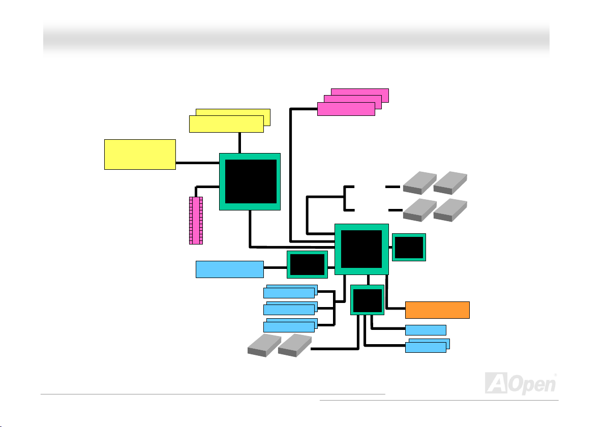
BBlloocckk DDiiaaggrraamm
Socket 478
Intel Pentium 4
CPU(Willamette
/Northwood)
PC100/PC133 SDRAM
SIMM Socket x2
MX46LS-V: 400MHz
System Bus
MX46LS-533V: 400/533MHz
System Bus
AGP 4X Slot
LAN connect Component
Floppy Disk Drive x2
Up to 1GB
MX46LS-V: SIS
650GX
MX46LS-533V:
SIS 651
USB2.0
port x6
PCI Bus
Realtek
LAN PHY
1stUSB Channel
2ndUSB Channel
rd
3
USB Channel
32-bit PCI Slot x3
ATA
66/100/133
Primar y
Channel
Secondary
Channel
SIS 962L
ITE
IT8705F
RealTek
AC97
CODEC
2Mbit Flash EEPROM
Parallel Port
Serial Port x2
IDE Drive x4
17
Page 18

l
l
MMXX4466LLSS--VV // MMXX4466LLSS--553333VV OOnnlliinnee MMaannuua
a
HHaarrddwwaarree IInnssttaallllaattiioonn
This chapter describes jumpers, connectors and hardware devices of this motherboard.
Note: Electrostatic discharge (ESD) can damage your processor, disk drives, expansion boards, and other
components. Always observe the following precautions before you install a system component.
1. Do not remove a component from its protective packaging until you are ready to install it.
2. Wear a wrist ground strap and attach it to a metal part of the system unit before handling a component. If
a wrist strap is not available, maintain contact with the system unit throughout any procedure requiring
ESD protection.
18
Page 19

l
l
MMXX4466LLSS--VV // MMXX4466LLSS--553333VV OOnnlliinnee MMaannuua
a
AAbboouutt ““UUsseerr UUppggrraaddee OOppttiioonnaall”” aanndd ““MMaannuuffaaccttuurree UUppggrraaddee OOppttiioonnaall””……
When you read this online manual and start to assemble your computer system, you may notice that some of the functions are marked as
“User Upgrade Optional” or “Manufacture Upgrade Optional”. Although all of AOpen’s motherboards have included many amazing and
powerful features, sometimes not every user is familiar with these powerful features. As a result of this we define features that can be
upgraded by users as “User Upgrade Optional”. You can upgrade these functions by purchasing additional devices. As for functions that
cannot be upgraded by users, we define them as “Manufacture Upgrade Optional”. If need be, you can contact our local distributors or
resellers to purchase “Manufacture Upgrade Optional” components, and again you are also welcome to visit our official website at
HTTP://english.aopen.com.tw
for detail information.
19
Page 20
l
l
MMXX4466LLSS--VV // MMXX4466LLSS--553333VV OOnnlliinnee MMaannuua
a
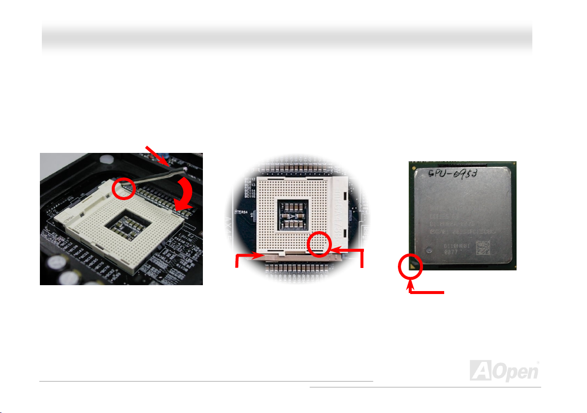
CCPPUU IInnssttaallllaattiioonn
This motherboard supports Intel® Pentium 4 Socket 478 series CPU (Willamette / Northwood). Be careful of CPU orientation when you plug
it into CPU socket.
1. Pull up the CPU socket lever and
up to 90-degree angle.
2. Locate Pin 1 in the socket and look for mark on the CPU upper interface.
Match Pin 1 and cut edge, then insert the CPU into the socket.
Note: Those pictures are for example only; they may not look the same with the motherboard you purchased.
CPU socket
Lever
CPU pin 1 and
cut edge
CPU cut edge
20
Page 21
l
l
y
MMXX4466LLSS--VV // MMXX4466LLSS--553333VV OOnnlliinnee MMaannuua
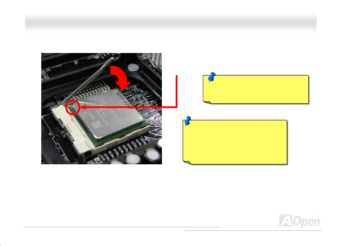
3. Press down the CPU socket lever and finish CPU
installation.
Note: This picture is for example only; it may not look the same with the motherboard you purchased.
CPU cut edge
Note: If you do not match the CPU
socket Pin 1 and CPU cut edge well, you
ma
damage the CPU.
Note: This socket supports
Micro-FC-PGA2 package CPU, which is
the latest CPU package developed by
Intel. Other forms of CPU package are
impossible to be fitted in.
a
21
Page 22
l
l
y
MMXX4466LLSS--VV // MMXX4466LLSS--553333VV OOnnlliinnee MMaannuua
a
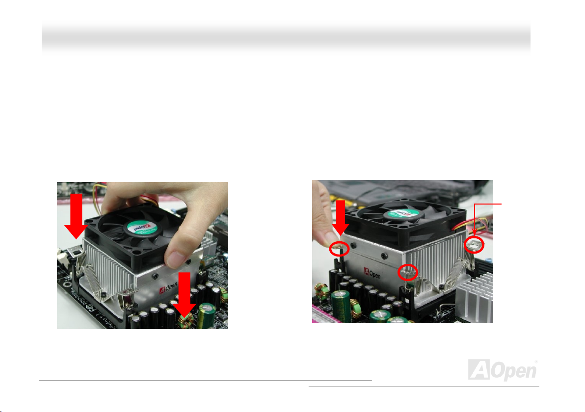
CCPPUU FFaann IInnssttaallllaattiioonn
This motherboard comes with a retention module attached on the CPU socket when shipped, we strongly recommend you to install AOpen
special designed CPU Fan as shown below on the retention module for better heat dissipation. Please install the CPU Fan correctly as the
following pictures shown.
1. Gently put the CPU Fan down on the
retention module with clips aligning correctl
to the four corners.
2. Pressing down the four clips with force one by one
on the retention module.
Clip
22
Page 23
l
l
MMXX4466LLSS--VV // MMXX4466LLSS--553333VV OOnnlliinnee MMaannuua
a
EEnnllaarrggeedd AAlluummiinnuumm HHeeaattssiinnkk
Cool down CPU and Chipset are important for system reliability. Enlarged aluminum heat sink provides better heat consumption especially
when you are trying to over-clock the CPU.
23
Page 24
l
l
MMXX4466LLSS--VV // MMXX4466LLSS--553333VV OOnnlliinnee MMaannuua
a
FFuullll--rraannggee AAddjjuussttaabbllee CCPPUU CCoorree VVoollttaaggee
This function is dedicated to overclockers and supports Adjustable CPU Core Voltage from 1.10V to 1.85V. However, this motherboard can
also automatically detect CPU VID signal and generates proper CPU core voltage.
SSeettttiinngg CCPPUU FFrreeqquueennccyy
BIOS Setup > Frequency/Voltage Control > CPU Clock Setting
This motherboard is CPU jumper-less design, you can set CPU frequency through the BIOS setup, and no jumpers or switches are needed.
The default setting is "table select mode". You can adjust the FSB from "CPU Host/SDRAM/PCI Clock" for overclocking.
Core Frequency = CPU FSB Clock * CPU Ratio
PCI Clock = CPU FSB Clock / Clock Ratio
AGP Clock = PCI Clock x 2
CPU Ratio
CPU FSB (By BIOS table)
8x, 10x… 21x, 22x, 23x, 24x
100 MHz
24
Page 25
l
l
A
MMXX4466LLSS--VV // MMXX4466LLSS--553333VV OOnnlliinnee MMaannuua
a
Northwood CPU
Pentium 4 1.6G 1600MHz 100MHz 400MHz 16x
Pentium 4 1.6G 1600MHz 133MHz 533MHz 12x
Pentium 4 1.7G 1700MHz 133MHz 533MHz 13x
Pentium 4 1.8G 1800MHz 100MHz 400MHz 18x
Pentium 4 2.0G 2000MHz 100MHz 400MHz 20x
Pentium 4 2.2G 2200MHz 100MHz 400MHz 22x
Pentium 4 2.26G 2260MHz 133MHz 533MHz 17x
Pentium 4 2.4G 2400MHz 100MHz 400MHz 24x
Pentium 4 2.4G 2400MHz 133MHz 533MHz 18x
Pentium 4 2.53G 2530MHz 133MHz 533MHz 19x
Pentium 4 2.66G 2660MHz 133MHz 533MHz 20x
Pentium 4 2.8G 2800MHz 133MHz 533MHz 21x
CPU Core
Frequency
FSB
Clock
System
Bus
Ratio
Warning: SIS 650GX / SIS 651 chipsets support
maximum 400MHz (100MHz*4) system bus and 66MHz
GP clock; higher clock setting may cause serious
system damage.
Willamette
CPU
Pentium 4
1.5G
Pentium 4
1.6G
Pentium 4
1.7G
Pentium 4
1.8G
Pentium 4
1.9G
Pentium 4
2.0G
Celeron
CPU
Celeron
1.7G
Celeron
1.8G
CPU Core
Frequency
1500MHz 100MHz 400MHz 15x
1600MHz 100MHz 400MHz 16x
1700MHz 100MHz 400MHz 17x
1800MHz 100MHz 400MHz 18x
1900MHz 100MHz 400MHz 19x
2000MHz 100MHz 400MHz 20x
CPU Core
Frequency
1700MHz 100MHz 400MHz 17x
1800MHz 100MHz 400MHz 18x
Note: Since the latest processor, Northwood,
would detect the clock ratio automatically,
you may not be able to adjust the clock ratio
in BIOS manually.
FSB
Clock
FSB
Clock
System
Bus
System
Bus
Ratio
Ratio
25
Page 26
l
l
MMXX4466LLSS--VV // MMXX4466LLSS--553333VV OOnnlliinnee MMaannuua
a
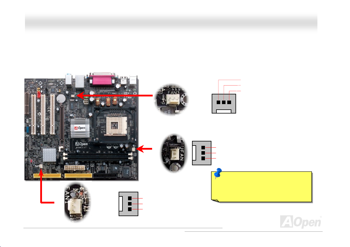
CCPPUU aanndd SSyysstteemm FFaann CCoonnnneeccttoorrss ((wwiitthh HH//WW MMoonniittoorriinngg))
Plug in the CPU fan cable to the 3-pin CPUFAN1 connector. If you have chassis fan, you can also plug it on SYSFAN2 or SYSFAN3
connector.
SYSFAN3 Connector
CPUFAN1 Connector
GND
+12V
SENSOR
Note: Some CPU fans do not have
sensor pin, so that they cannot support
hardware monitoring function.
GND
+12V
SENSOR
GND
+12V
NC
SYSFAN2 Connector
26
Page 27
l
l
MMXX4466LLSS--VV // MMXX4466LLSS--553333VV OOnnlliinnee MMaannuua
a
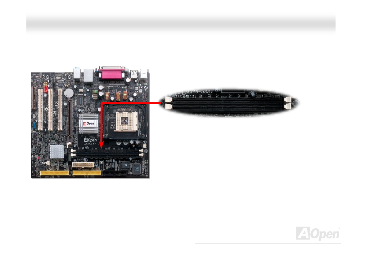
DDIIMMMM SSoocckkeettss
This model has two 168-pin DIMM sockets that allow you to install PC100/PC133 memory up to 1GB.
DIMM1
DIMM2
27
Page 28
l
l
MMXX4466LLSS--VV // MMXX4466LLSS--553333VV OOnnlliinnee MMaannuua
a
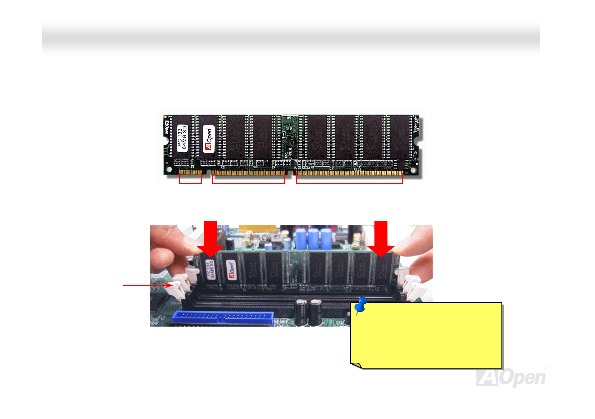
HHooww ttoo IInnssttaallll MMeemmoorryy MMoodduulleess
Please follow the procedure as shown below to finish memory installation.
1. Make sure the SIMM module’s pin face down and match the socket’s size as depicted below.
2. Insert the module straight down to the SIMM slot with both hands and press down firmly until the SIMM module is securely in place.
3. Repeat step 2 to finish additional SIMM modules installation.
Ta b
20 pins 60 pins 88 pins
Note: The tabs of the SIMM slot
will close-up to hold the SIMM in
place when the SIMM touches the
slot’s bottom.
28
Page 29

l
l
e
&
r
r
A
A
MMXX4466LLSS--VV // MMXX4466LLSS--553333VV OOnnlliinnee MMaannuua
a
FFrroonntt PPaanneell CCoonnnneeccttoorr
Pin1
Attach the power LED, Keylock, speaker, power and reset switch connectors to th
corresponding pins. If you enable “Suspend Mode” item in BIOS Setup, the ACPI
Power LED will keep flashing while the system is in suspend mode.
Locate the power switch cable from your ATX housing. It is 2-pin female connecto
from the housing front panel. Plug this connector to the soft-power switch connecto
marked SPWR.
Suspend Type ACPI LED
Power on Suspend (S2) or Suspend to RAM (S3) Flashing for every second
Suspend to Disk (S4) The LED will be turned off
IDE LED
Speaker
1
SPWR
CPI & PWR
LED
CPI LED (BLUE)
Reset
SPEAKER
NC
NC
+5V
IDE LED
IDE LED
+5V
+5V
GND
NC
1
SPWR
GND
ACPI LED GND
ACPILED
NC
ACPI_B
GND
RESET
GND
29
Page 30

l
l
MMXX4466LLSS--VV // MMXX4466LLSS--553333VV OOnnlliinnee MMaannuua
a
AATTXX PPoowweerr CCoonnnneeccttoorr
This motherboard comes with a 20-pin and 4-pin ATX power connector. Make sure you plug in the right direction. We strongly recommend
you to connect the 4-pin 12V ATX connector before connecting the 20-pin ATX power connector and use standard power supply specially
designed for Pentium 4 system.
AACC PPoowweerr AAuuttoo RReeccoovveerryy
A traditional ATX system should remain at power off stage when AC power resumes from power failure. This design is inconvenient for a
network server or workstation, without an UPS, that needs to keep power-on. This motherboard implements an AC Power Auto Recovery
function to solve this problem.
Ground
Ground
12V
12v
30
Page 31

l
l
MMXX4466LLSS--VV // MMXX4466LLSS--553333VV OOnnlliinnee MMaannuua
a
IIDDEE aanndd FFllooppppyy CCoonnnneeccttoorr
Connect 34-pin floppy cable and 40-pin IDE cable to floppy connector FDD and IDE connector. Be careful of the pin1 orientation. Wrong
orientation may cause system damage.
IDE 2 (Secondary)
ATA 66/100/133
IDE Connector
IDE 1 (Primary)
Pin 1
ATA 66/100/133
IDE Connector
FDD Connector
31
Page 32

l
l
MMXX4466LLSS--VV // MMXX4466LLSS--553333VV OOnnlliinnee MMaannuua
IDE1 is also known as the primary channel and IDE2 as the secondary channel. Each channel supports two IDE devices that make a total
of four devices. In order to work together, the two devices on each channel must be set differently to Master and Slave mode. Either one
can be the hard disk or the CDROM. The setting as master or slave mode depends on the jumper on your IDE device, so please refer to
your hard disk and CDROM manual accordingly.
Tip:
1. For better signal quality, it is recommended to set the far end side device to
master mode and follow the suggested sequence to install your new device.
Please refer to above diagram
2. To achieve the best performance of ATA133 hard disks, a special 80-wires IDE
Warning: The specification of the IDE cable is a maximum of 46cm (18 inches);
make sure your cable does not exceed this length.
a
32
Page 33

l
l
MMXX4466LLSS--VV // MMXX4466LLSS--553333VV OOnnlliinnee MMaannuua
a
AATTAA113333 SSuuppppoorrtteedd
This motherboard supports ATA66 , ATA100 or ATA133 IDE devices. Following table lists the transfer rate of IDE PIO and DMA modes. The
IDE bus is 16-bit, which means every transfer is two bytes. As the hard drive industry introduces faster and higher capacity hard drives,
the current Ultra ATA/100 interface causes a data bottleneck between the drive and the host computer. To avoid this problem, hard disk
manufactures have introduced the new Ultra ATA-133 interface technology.
percent increase in interface speed with transfer rate of 133MB/s. ATA/133 performance is ideal for new operating systems, such as
Window XP, that demand more storage space and faster data transfer rates from more responsive computing experiences.
To make good use of this new technology and enjoy its best performance, we recommend you to pair your system with a hard disk
equipped with ATA/133 technology so that your system's need for speed on this motherboard can be satisfied.
Compared to traditional ATA/100, ATA/133 has up to 33
Mode Clock Period Clock Count Cycle Time Data Transfer Rate
PIO mode 0 30ns 20 600ns (1/600ns) x 2byte = 3.3MB/s
PIO mode 1 30ns 13 383ns (1/383ns) x 2byte = 5.2MB/s
PIO mode 2 30ns 8 240ns (1/240ns) x 2byte = 8.3MB/s
PIO mode 3 30ns 6 180ns (1/180ns) x 2byte = 11.1MB/s
PIO mode 4 30ns 4 120ns (1/120ns) x 2byte = 16.6MB/s
DMA mode 0 30ns 16 480ns (1/480ns) x 2byte = 4.16MB/s
DMA mode 1 30ns 5 150ns (1/150ns) x 2byte = 13.3MB/s
DMA mode 2 30ns 4 120ns (1/120ns) x 2byte = 16.6MB/s
ATA 66 30ns 2 60ns (1/60ns) x 2byte x2 = 66MB/s
ATA 100 20ns 2 40ns (1/40ns) x 2byte x2 = 100MB/s
ATA 133 15ns 2 30ns (1/30ns) x 2byte x2= 133MB/s
33
Page 34

l
l
MMXX4466LLSS--VV // MMXX4466LLSS--553333VV OOnnlliinnee MMaannuua
a
IIrrDDAA CCoonnnneeccttoorr
The IrDA connector can be configured to support wireless infrared module, with this module and application software such as Laplink or
Windows 95 Direct Cable Connection, the user can transfer files to or from laptops, notebooks, PDA devices and printers. This connector
supports HPSIR (115.2Kbps, 2 meters) and ASK-IR (56Kbps).
Install the infrared module onto the IrDA connector and enable the infrared function from BIOS Setup, UART Mode, make sure to have the
correct orientation when you plug in the IrDA connector.
NC
+5V
IR_TX
IIrrDDAA CCoonnnneeccttoorr
KEY
GND
IR_RX
Pin 1
34
Page 35

l
l
MMXX4466LLSS--VV // MMXX4466LLSS--553333VV OOnnlliinnee MMaannuua
a
AAGGPP ((AAcccceelleerraatteedd GGrraapphhiicc PPoorrtt)) EExxppaannssiioonn SSlloott
MX46LS-V / MX46LS-533V provides an AGP 4x slot. The AGP 4x is a bus interface targeted for high-performance 3D graphic. AGP
supports only memory read/write operation and single-master single-slave one-to-one only. AGP uses both rising and falling edge of the
66MHz clock, for 2X AGP, the data transfer rate is 66MHz x 4bytes x 2 = 528MB/s. AGP is now moving to AGP 4x mode, 66MHz x 4bytes x
4 = 1056MB/s.
35
Page 36

l
l
MMXX4466LLSS--VV // MMXX4466LLSS--553333VV OOnnlliinnee MMaannuua
a
WWOOLL ((WWaakkee oonn LLAANN))
To use Wake On LAN function, you must have a network card with chipset that supports this feature, and connect a cable from LAN card to
motherboard WOL connector. The system identification information (probably IP address) is stored on network card and because there is a
lot of traffic on the Ethernet, you need to install network management software, such as ADM, for the checking of how to wake up the
system. Note that, at least 600mA ATX standby current is required to support the LAN card for this function.
WOL connector
LID
GND
+5VSB
36
Page 37

l
l
MMXX4466LLSS--VV // MMXX4466LLSS--553333VV OOnnlliinnee MMaannuua
WOL Connector
(Motherboard Side)
Note: This picture is for example only; it may not exactly look the same with the motherboard you purchased.
WOL Connector
(Ethernet Card Side)
a
37
Page 38

l
l
MMXX4466LLSS--VV // MMXX4466LLSS--553333VV OOnnlliinnee MMaannuua
a
SSuuppppoorrtt 1100//110000 MMbbppss LLAANN oonnbbooaarrdd
On the strength of integrated SiS LAN controller with Realtek PHY on board, which is a highly-integrated Platform LAN Connect device, it
provides 10/100M bps Ethernet for office and home use, the Ethernet RJ45 connector is located on top of USB connectors. The green LED
indicates the link mode, it lights when linking to network and blinking when transferring data. The orange LED indicates the transfer mode
and it lights when data is transferring in 100Mbps mode. To enable or disable this function, you may simply adjust it through BIOS.
Green/10M ACT/LNK
Orange/100M ACT/LNK
38
Page 39

l
l
MMXX4466LLSS--VV // MMXX4466LLSS--553333VV OOnnlliinnee MMaannuua
a
CCNNRR ((CCoommmmuunniiccaattiioonn aanndd NNeettwwoorrkk RRiisseerr)) EExxppaannssiioonn SSlloott
CNR is a riser card specification to replace the AMR (Audio/Modem Riser) that supports V.90 analog modem, multi-channel audio, and
phone-line based networking. Owing to CPU computing power getting stronger, the digital processing job can be implemented in main
chipset and share CPU power. The analogy conversion (CODEC) circuit requires a different and separate circuit design, which is put on
CNR card. This motherboard implements sound CODEC on board, but reserve CNR slot for the option of modem function. Note that you
can still use PCI modem card.
39
Page 40

l
l
V
Y
MMXX4466LLSS--VV // MMXX4466LLSS--553333VV OOnnlliinnee MMaannuua
a
SSuuppppoorrtt TThhrreeee UUSSBB22..00 CChhaannnneellss ((SSiixx PPoorrttss))
This motherboard provides 6 USB2.0 ports to connect USB devices such as mouse, keyboard, modem, printer, etc. There are four ports on
the PC99 back panel. You can use proper cables to connect USB devices from PC99 back panel or connect 3
front panel of chassis.
Compared to traditional USB 1.0/1.1 with the speed of 12Mbps, USB 2.0 has a fancy speed up to 480Mbps that is 40 times faster than the
traditional one. Except for the speed increase, USB 2.0 supports old USB 1.0/1.1 software and peripherals, offering impressive and even
better compatibility to customers. On this motherboard, all six ports support USB 2.0 function.
SBD2-
SBD2+
+5
GND
KE
1
+5V
SBD3SBD3+
GND
NC
Pin 1
rd
USB Channel
3
nd
2
USB Channel
rd
USB channel header to the
1st USB Channel
40
Page 41

l
l
MMXX4466LLSS--VV // MMXX4466LLSS--553333VV OOnnlliinnee MMaannuua
a
CCoolloorr CCooddeedd BBaacckk PPaanneell
The onboard I/O devices are PS/2 Keyboard, PS/2 Mouse, RJ-45 LAN Connector, COM1 and VGA, Printer, USB and AC97 sound. The
view angle of drawing shown here is from the back panel of the housing.
PS/2 Keyboard: For standard keyboard, which is using a PS/2 plug.
PS/2 Mouse: For PC-Mouse, which is using a PS/2 plug.
USB Port: Available for connecting USB devices.
Parallel Port: To connect with SPP/ECP/EPP printer.
COM1/COM2 Port: To connect with pointing devices, modem or others serial devices.
RJ-45 LAN connector To connect Ethernet for home or office use.
VGA Connector: To connect with PC monitor.
Speaker Out: To External Speaker, Earphone or Amplifier.
Line-In: Comes from the signal sources, such as CD/Tape player.
MIC-In: From Microphone.
PS/2 Mouse
Connector
PS/2 Keyboard
Connector
USB2.0
Port
COM 1 Port
SPP/EPP/ECP
Parallel Port
VGA Port
RJ-45 LAN
Connector
USB2.0 Port
Line-In
Speaker Out
MIC-In
41
Page 42

l
l
MMXX4466LLSS--VV // MMXX4466LLSS--553333VV OOnnlliinnee MMaannuua
a
CCaassee OOppeenn CCoonnnneeccttoorr
The “CASE OPEN” header provides chassis intrusion-monitoring function. To make this function works, you have to enable it in the system
BIOS, connect this header to a sensor somewhere on the chassis. So, whenever the sensor is triggered by lights or by the opening of the
chassis, the system will beep to inform you. Please be informed that this useful function only applies to advanced chassis, you may
purchase an extra sensor, attach it on your chassis, and make a good use of this function.
Pin 1
Sensor
GND
42
Page 43

l
l
MMXX4466LLSS--VV // MMXX4466LLSS--553333VV OOnnlliinnee MMaannuua
a
CCDD AAuuddiioo CCoonnnneeccttoorr
This connector is used to connect CD Audio cable from CDROM or DVD drive to onboard sound.
CD-IN
R
GND
GND
L
Note: Though some of the latest versions of Windows
support “Digital Audio” through IDE bus. However, in
order to use Open Jukebox player, which is driven under
BIOS, it is a MUST to connect audio cable to CD-IN
connector on the motherboard.
43
Page 44

l
l
MMXX4466LLSS--VV // MMXX4466LLSS--553333VV OOnnlliinnee MMaannuua
a
MMOODDEEMM--IINN CCoonnnneeccttoorr
The MODEM-CN connector is used to connect Mono In/ Mic Out cable from internal modem card to onboard sound circuit.
MIC OUT
GND
GND
MONO IN
MODEM-CN Connector
44
Page 45

l
l
#
#
#
MMXX4466LLSS--VV // MMXX4466LLSS--553333VV OOnnlliinnee MMaannuua
a
CCOOMM22 CCoonnnneeccttoorr
This motherboard provides two serial ports. One of them are on back panel connector, the other is on the middle left between PCI slots.
With proper cable, you can connect it to the back panel of chassis.
1 2
DCD
SOUT
GND
RI
RTS
Pin 1
SIN
DTR#
DSR#
CTS#
45
Page 46

l
l
p
A
A
A
A
MMXX4466LLSS--VV // MMXX4466LLSS--553333VV OOnnlliinnee MMaannuua
a
FFrroonntt AAuuddiioo CCoonnnneeccttoorr
If the housing has been designed with an audio port on the front panel, you’ll be able to connect onboard audio to front panel through this
connector. By the way, please remove the jumper cap from the Front Audio Connector before you connect the cable. Do not remove this
yellow jumper cap if your housing doesn’t have an audio port on the front panel.
Pin 1
NC
1
UD_GND
UD_VCC
UD_RET_R
KEY
UD_RET_L
ort on the front panel.
AUD_MIC
AUD_MIC_BIAS
AUD_FPOUT_R
AUD_FPOUT_L
Note: Please remove the jumper cap from the front audio connector before you
connect the cable. Do not remove this yellow jumper cap if your housing doesn’t
have an audio
46
Page 47

l
l
A
MMXX4466LLSS--VV // MMXX4466LLSS--553333VV OOnnlliinnee MMaannuua
a
SS//PPDDIIFF ((SSoonnyy//PPhhiilliippss DDiiggiittaall IInntteerrffaaccee)) CCoonnnneeccttoorr
S/PDIF (Sony/Philips Digital Interface) is a latest audio transfer file format that provides impressive quality through optical fiber and allows
you to enjoy digital audio instead of analog. Normally there are two S/PDIF outputs as shown, one for RCA connector, the most common
one used for consumer audio products, and the other for optical connector with a even better audio quality. Through a specific audio cable,
you can connect the S/PDIF connector to a S/PDIF audio module bearing S/PDIF digital output. However, you must have a S/PDIF
supported speaker with S/PDIF digital input to make the most of this function.
1
+5V
NC
SPDIFOUT
GND
SPDIFIN
5
Connecting to
Connecting to
Optical Cable
Pin 1
S/PDIF
Connector
udio cable
S/PDIF Module
(Optional)
47
Page 48

l
l
(
)
MMXX4466LLSS--VV // MMXX4466LLSS--553333VV OOnnlliinnee MMaannuua
a
JJPP1144 CClleeaarr CCMMOOSS DDaattaa
You can clear CMOS to restore system default setting. To clear CMOS, follow the procedure below.
1. Turn off the system and unplug the AC power.
2. Remove ATX power cable from connector PWR2.
3. Locate JP14 and short pins 2-3 for a few seconds.
4. Return JP14 to its normal setting by shorting pin 1 & pin 2.
5. Connect ATX power cable back to connector PWR2.
Normal
default
Clear CMOS
Pin 1
Tip: When should I Clear CMOS?
1. Boot fail because of overclocking…
2. Forget password…
3. Troubleshooting…
48
Page 49

l
l
MMXX4466LLSS--VV // MMXX4466LLSS--553333VV OOnnlliinnee MMaannuua
a
JJPP2288 UUSSBB KKeeyybbooaarrdd//MMoouussee WWaakkee--uupp EEnnaabbllee//DDiissaabbllee JJuummppeerr
This motherboard provides keyboard / mouse wake-up function. You can use JP28 to enable or disable this function, which could resume
your system from suspend mode with keyboard or mouse installed. JP28 controls both 1
default setting is set to “Disable”(1-2), and you may enable this function by setting the jumper to 2-3.
Pin 1
2nd USB Channel
JP28
KB/Mouse Wake-up
Disable
(Default)
Enable
st
and 2nd USB channel and PS2 port. The factory
st
USB Channel
1
49
Page 50

l
l
MMXX4466LLSS--VV // MMXX4466LLSS--553333VV OOnnlliinnee MMaannuua
a
AAOOppeenn ““WWaattcchh DDoogg TTiimmeerr””
With this motherboard, AOpen provides a very special, useful feature for overclockers. When you power-on
the system, the BIOS will check last system POST
Timer” function immediately, and set the CPU FSB
system failed in BIOS POST, the “Watch Dog Timer” will reset the system to reboot in five seconds. Then,
BIOS will detect the CPU’s default frequency and POST again. With this special feature, you can easily
overclock your system to get higher system performance, and without removing the cover of system housing to set the jumper to clear
CMOS data when your system hanged.
AOpen
Watch Dog Timer
Enable/Disable Signal from
BIOS
Countdown about
5 seconds if fails
in POST
Reset Signal
Clock Generator
status. If it succeeded, the BIOS will enable “Watch Dog
frequency by user’s setting that stored in the BIOS. If
BIOS
CPU ID Signal
CPU
50
Page 51

l
l
r
A
A
MMXX4466LLSS--VV // MMXX4466LLSS--553333VV OOnnlliinnee MMaannuua
a
BBaatttteerryy--lleessss aanndd LLoonngg LLiiffee DDeessiiggnn
This Motherboard implements a Flash ROM and a special circuit that provide you no batter power consumption of current CPU and CMOS
Setup configurations. The RTC (real time clock) can also keep running as long as the power cord is plugged. If you lose your CMOS data
by accident, you can just reload the CMOS configurations from Flash ROM and the system will recover as usual.
ATX Stand-by Powe
Battery
Flash ROM
(Real Time Clock)
Auto Switch
RTC
00:00:00
CMOS
uto switching to ATX standby power as long as
C power line is plugged. This smart design
increases battery life if you still plug battery on
motherboard.
Backup by EEPROM
51
Page 52

l
l
MMXX4466LLSS--VV // MMXX4466LLSS--553333VV OOnnlliinnee MMaannuua
a
OOvveerr--ccuurrrreenntt PPrrootteeccttiioonn
The Over Current Protection is a popular implementation on ATX 3.3V/5V/12V switching power supply. However, the new generation CPU
uses different voltage with a regulator to transfer 12V to CPU voltage (for example, 2.0V), and thus makes 5V over current protection
useless. This motherboard is with switching regulator onboard supporting CPU over-current protection; in conjunction with 3.3V/5V/12V
power supply provide the full line over-current protection.
ATX Switching Power Supply
Note: Although we have implemented protection circuit and tried to prevent any human operating
mistake, certain risks might still happen when CPU, memory, HDD or add-on cards installed on this
motherboard is damaged due to component failure, human operating error or other unknown natural
reasons. AOpen cannot guarantee that the protection circuit will always work perfectly.
3.3V (Protected by power supply)
5V (Protected by power supply)
12V (Protected by power supply)
Onboard
Power
Regulator
Over-Current
Protection
Circuit
CPU Core Voltage
52
Page 53

l
l
MMXX4466LLSS--VV // MMXX4466LLSS--553333VV OOnnlliinnee MMaannuua
a
RReesseettaabbllee FFuussee
Traditional motherboard uses fuses to prevent Keyboard and USB port from over-current or shortage. These fuses are soldered onboard
that when it is broken (function to protect motherboard), user cannot replace them and result in malfunction of motherboard.
With expensive Resetable Fuse, the motherboard can be resumed back to normal function even after the fuse had done its protection job.
Resettable
Fuse
53
Page 54

l
l
MMXX4466LLSS--VV // MMXX4466LLSS--553333VV OOnnlliinnee MMaannuua
a
LLooww EESSRR CCaappaacciittoorr
The quality of low ESR capacitor (Low Equivalent Series Resistance) during high frequency operation is very important for the stability of
CPU power. The idea of where to put these capacitors is another know-how that requires experience and detail calculation.
Not only that, MX46LS-V / MX46LS-533V implements 2200μF capacitors, which is much larger than normal capacitor (1000 & 1500μF)
and it provides better stability for CPU power.
54
Page 55

l
l
MMXX4466LLSS--VV // MMXX4466LLSS--553333VV OOnnlliinnee MMaannuua
The power circuit of the CPU core voltage must be checked to ensure system stability for high speed CPUs (such as the new Pentium III, or
when overclocking). A typical CPU core voltage is 2.0V, so a good design should control voltage between 1.860V and 2.140V. That is, the
transient must be below 280mV. Below is a timing diagram captured by a Digital Storage Scope, it shows the voltage transient is only
143mv even when maximum 60A current is applied.
Note: This diagram for example only, it may not be exactly the same as the motherboard you purchased.
a
55
Page 56

l
l
MMXX4466LLSS--VV // MMXX4466LLSS--553333VV OOnnlliinnee MMaannuua
a
PPhhooeenniixx--AAWWAARRDD BBIIOOSS
System parameters can be modified by going into BIOS Setup menu, this menu allows you to configure the system parameters and save
the configuration into the 128 bytes CMOS area, (normally in the RTC chip or in the main chipset).
Phoenix-AwardBIOS™ installed in the Flash ROM
provides critical low-level support for standard devices such as hard disk drives, serial and parallel ports.
Most BIOS settings of this model have been optimized by AOpen’s R&D engineering team. But, the default setting of BIOS still can’t
fine-tune the chipset controlling entire system. Therefore, the rest of this chapter intends to guide you the process of configuring your
system setup.
To enter to BIOS setup menu
, press <Del> when POST (Power-On Self Test) screen is shown on your monitor.
Note: Because the BIOS code is the most often
changed part of the motherboard design, the BIOS
information contained in this manual may be different
with actual BIOS that come with your motherboard.
of the motherboard is a custom version of an industry standard BIOS. The BIOS
56
Page 57

l
l
MMXX4466LLSS--VV // MMXX4466LLSS--553333VV OOnnlliinnee MMaannuua
a
AAbboouutt BBIIOOSS FFuunnccttiioonn DDeessccrriippttiioonn……
AOpen always dedicates to give user a friendlier computer system. Now, we include all function descriptions of BIOS setup program into
the BIOS Flash ROM. When you select one function of BIOS setup program, the function description will appear at the right side of screen.
Therefore, you don’t need to read this manual while you change BIOS settings.
Menu Items Select Window Item Function Description Window
57
Page 58

l
l
MMXX4466LLSS--VV // MMXX4466LLSS--553333VV OOnnlliinnee MMaannuua
a
HHooww TToo UUssee PPhhooeenniixx--AAwwaarrdd™™ BBIIOOSS SSeettuupp PPrrooggrraamm
Generally, you can use arrow keys to highlight items that you want to choose, then press <Enter> key to select, and use the <Page Up>
and <Page Down> key to change setting values. You can also press <F1> key for help and press <Esc> key to quit Phoenix-Award™ BIOS
setup program. The following table provides details about how to use keyboard in the Phoenix-Award™ BIOS setup program. By the way,
all products of AOpen also provide a special function in BIOS setup; you can press <F3> key selecting you preferred menu language.
Key Description
Page Up or + Changing setting to next value or increase the value.
Page Down or - Changing setting to previous value or decrease value.
Enter Select the item.
Esc 1. In main menu: Quit and don’t save any change.
2. In sub menu: Exit current menu to main menu.
Up Arrow Highlight previous item.
Down Arrow Highlight next item.
Left Arrow Move the light bar to left side of menu.
Right Arrow Move the light bar to right side of menu.
F1 Get menu or item help description.
F3 Changing menu language.
F5 Load previous setting value from CMOS.
58
Page 59

l
l
MMXX4466LLSS--VV // MMXX4466LLSS--553333VV OOnnlliinnee MMaannuua
Key Description
F6 Load fail-save setting value from CMOS.
F7 Load turbo setting value from CMOS.
F10 Save changed setting and exit setup program.
a
59
Page 60

l
l
MMXX4466LLSS--VV // MMXX4466LLSS--553333VV OOnnlliinnee MMaannuua
a
HHooww TToo EEnntteerr BBIIOOSS SSeettuupp
After you finish jumper settings and connect correct cables, power on and enter the BIOS Setup. Press <Del> during POST (Power-On Self
Te st ) and choose "Load Setup Defaults" for recommended optimal performance.
Del
Warning: Please avoid of using "Load Turbo Defaults", unless you
are sure your system components (CPU, DRAM, HDD, etc.) are
good enough for turbo setting.
60
Page 61

l
l
p
MMXX4466LLSS--VV // MMXX4466LLSS--553333VV OOnnlliinnee MMaannuua
a
BBIIOOSS UUppggrraaddee uunnddeerr WWiinnddoowwss eennvviirroonnmmeenntt
With outstanding R&D ability of AOpen, we now bring you a whole new BIOS Flash wizard ----
EzWinFlash. With an eye to users’ convenience, EzWinFlash combines the BIOS binary code
and flash module together, so the only thing you have to do is just clicking on the utility you downloaded from web and let it helps you
complete the flash process automatically. EzWinFlash detects your motherboard and checks the BIOS version cleverly to prevent your
system from any possible failure. Moreover, EzWinFlash has been taken into consideration to go with any windows platform you might be
using, no matter if you’re using Windows 95/98, 98SE/ME, NT4.0/2000, or even the latest Windows XP.
In the meanwhile, in order to provide a much more user-friendly operating environment, AOpen EzWinFlash is natively designed to have
multi-language function to provide easier way for users’ usage in changing BIOS setting.
Caution: By updating your motherboard,
you are taking a risk of BIOS flash failure. If
your motherboard is working stable, and
there are no major bugs that had been fixed
by a latter BIOS revision, we recommend
that you DO NOT try to upgrade your BIOS.
If you intent on upgrading, PLEASE BE
SURE to get the right BIOS revision for the
right motherboard model to avoid any
ossibility failure.
61
Page 62

l
l
MMXX4466LLSS--VV // MMXX4466LLSS--553333VV OOnnlliinnee MMaannuua
You may accomplish BIOS upgrade procedure with EzWinFlash by the following steps, and it’s STRONGLY RECOMMMANDED to close all
the applications before you start the upgrading.
1. Download the new version of BIOS package zip
2. Unzip the download BIOS package (ex: WMX46LSV102.ZIP) with WinZip (http://www.winzip.com
3. Save the unzipped files into a folder, for example, WMX46533V102.EXE & WMX46LSV102.BIN.
4. Double click on the WMX46LSV102.EXE, EzWinFlash will detect the model name and BIOS version of your motherboard. If you had
got the wrong BIOS, you will not be allowed to proceed with the flash steps.
5. You may select preferred language in the main menu, then click [Start Flash] to start the BIOS upgrade procedure.
6. EzWinFlash will complete all the process automatically, and a dialogue box will pop up to ask you to restart Windows. You may click
[YES] to reboot Windows.
7. Press <Del> at POST to enter BIOS setup
It is strongly recommended NOT to turn off the power or run any application during FLASH PROCESS.
Warning: The new BIOS upgrade will permanently replace your
original BIOS’s settings when flashing. You may need to reconfigure
your BIOS setting so that your system can go back to work as normal.
file from AOpen official web site. (ex: http://english.aopen.com.tw)
) in Windows environment.
, choose "Load Setup Defaults", then “Save & Exit Setup”. Done!
a
62
Page 63

l
l
MMXX4466LLSS--VV // MMXX4466LLSS--553333VV OOnnlliinnee MMaannuua
a
DDrriivveerr aanndd UUttiilliittyy
There are motherboard drivers and utilities in AOpen Bonus CD. You don’t need to install all of them to boot your system. But after you
finish the hardware installation, you have to install your operation system first (such as Windows 98) before you install any drivers or utilities.
Please refer to your operation system’s installation guide.
AAuuttoo--rruunn MMeennuu ffrroomm BBoonnuuss CCDD
You can use the auto-run menu of Bonus CD. Choose the utility and driver and select model name.
63
Page 64

l
l
MMXX4466LLSS--VV // MMXX4466LLSS--553333VV OOnnlliinnee MMaannuua
a
IInnssttaallll IIDDEE DDrriivveerr
To use IDE devices you have to install IDE driver from Bonus Pack CD.
64
Page 65

l
l
MMXX4466LLSS--VV // MMXX4466LLSS--553333VV OOnnlliinnee MMaannuua
a
IInnssttaalllliinngg AAGGPP DDrriivveerr
You can find AGP driver from the Bonus Pack CD auto-run menu.
65
Page 66

l
l
MMXX4466LLSS--VV // MMXX4466LLSS--553333VV OOnnlliinnee MMaannuua
a
IInnssttaalllliinngg VVGGAA DDrriivveerr
SiS 650GX/651 supports VGA on this motherboard. You can install VGA driver form the Bonus Pack CD.
66
Page 67

l
l
MMXX4466LLSS--VV // MMXX4466LLSS--553333VV OOnnlliinnee MMaannuua
a
IInnssttaallll UUSSBB22..00 DDrriivveerr
In Bonus Pack CD, you can install USB2.0 driver from the following screen.
67
Page 68

l
l
MMXX4466LLSS--VV // MMXX4466LLSS--553333VV OOnnlliinnee MMaannuua
a
IInnssttaalllliinngg LLAANN DDrriivveerr
You can download LAN Driver from the Bonus Pack CD.
68
Page 69

l
l
MMXX4466LLSS--VV // MMXX4466LLSS--553333VV OOnnlliinnee MMaannuua
a
IInnssttaalllliinngg OOnnbbooaarrdd SSoouunndd DDrriivveerr
This motherboard comes with AC97 CODEC. This audio driver supports Windows 98SE and upper Windows OS; you can find the audio
driver from the Bonus Pack CD auto-run menu.
69
Page 70

l
l
MMXX4466LLSS--VV // MMXX4466LLSS--553333VV OOnnlliinnee MMaannuua
a
AAOOCCoonnffiigg UUttiilliittyy
AOpen always dedicated to provide users a much friendly computer environment. We now bring you a comprehensive system detection
utility. AOConfig is a Windows based utility with user-friendly interface that allows users to obtain information of the operation system and
hardware such as motherboard, CPU, memory, PCI devices and IDE devices. The powerful utility also displays the version of BIOS and
firmware for your convenience of maintenance.
Moreover, AOConfig allows users to save information in *.BMP or *.TXT format which users may collect the system information in detail and
send them to AOpen directly for technical support or for further diagnose of system problems.
1. The system page shows the
detailed information of the
motherboard, operating
system, processor, and
BIOS version.
2. The PCI device page shows
the configurations of all PCI
devices installed in your
motherboard.
70
Page 71

l
l
MMXX4466LLSS--VV // MMXX4466LLSS--553333VV OOnnlliinnee MMaannuua
3. This page presents the IDE
device information, such as
serial number, manufacturer,
firmware version, and capacity.
4. From this page, users can
obtain the technical support
information of AOpen. Moreover,
detailed information could be
saved in .bmp or .txt format.
NOTE:
AOConfig can be used under Windows 98SE/ME, NT4.0/2000, or even the latest Windows XP. Please also note that
AOConfig can only be operated in a system equipped with an AOpen motherboard. Before running AOConfig, all
applications must be closed.
a
71
Page 72

l
l
MMXX4466LLSS--VV // MMXX4466LLSS--553333VV OOnnlliinnee MMaannuua
a
IInnssttaalllliinngg HHaarrddwwaarree MMoonniittoorriinngg UUttiilliittyy
You can install Hardware Monitoring Utility to monitor CPU temperature, fans and system voltage. The hardware monitoring function is
automatically implemented by BIOS and utility software. No hardware installation is needed.
72
Page 73

l
l
MMXX4466LLSS--VV // MMXX4466LLSS--553333VV OOnnlliinnee MMaannuua
a
GGlloossssaarryy
AACC9977 CCOODDEECC
Basically, AC97 CODEC is the standard structure of PCI sound card. As we know, computer is digital-based, but music is based on
analog-based. Therefore, there must be a process to turn digital into analog during the last stage processing of sound in computer.
Hence, the component on sound card that play this important task is what we called CODEC.
Audio CODEC 97 (briefly called AC97) is the specification regulated by Intel, and it’s about the structure of audio conversion. The
special place about CODEC is that it is separated from sound card (CODEC is an independent chipset). Therefore, PCI sound card
could possess with 90db and do other application process as well. We called CODEC that meets this structure AC97 CODEC.
AACCPPII ((AAddvvaanncceedd CCoonnffiigguurraattiioonn && PPoowweerr IInntteerrffaaccee)
ACPI is the power management specification of PC97 (1997). It intends to save more power by taking full control of power
management to operating system and bypass BIOS
operating system (such as Windows 98). This is a bit similar as the PnP
switch to control the power state transition.
AACCRR ((AAddvvaanncceedd CCoommmmuunniiccaattiioonn RRiisseerr)
Building on the PC motherboard riser architecture, ACR slot is backward compatible with AMR but beyond the limitation of it. The
ACR specification is designed to support modem, audio, Local Area Network (LAN) and Digital Subscriber Line (DSL).
)
. The chipset or super I/O chip needs to provide standard register interface to
register interface. ACPI defines ATX momentary soft power
)
73
Page 74

l
l
MMXX4466LLSS--VV // MMXX4466LLSS--553333VV OOnnlliinnee MMaannuua
)
AAGGPP ((AAcccceelleerraatteedd GGrraapphhiicc PPoorrtt)
The main function of AGP simply put is to tell monitor what screen information had to be shown, a visual transmission device
actually. With the rapid developing of AGP card, we can see that it had been developed from single colorful AGP card to 2D and 3D
graphic. AGP supports only memory read/write operation and single-master single-slave one-to-one only. Though AGP and PCI
share the same algorithm of 32-bit, its frequencies are 66MHz and 33MHz respectively. AGP interface had been developed from
2X to 8x.
1X AGP, data transfer rate is 66MHz x 4byte x 1 = 264MB/s
2X AGP, data transfer rate is 66MHz x 4byte x 2 = 528MB/s
4X AGP, data transfer rate is 66MHz x 4byte x 4 = 1056MB/s.
8X AGP, data transfer rate is 66MHz x 4byte x 8 = 2112MB/s.
AAMMRR ((AAuuddiioo//MMooddeemm RRiisseerr)
The CODEC circuit of AC97 sound/modem solution can be put on motherboard or put on a riser card (AMR card) that connects to
motherboard through AMR connector.
)
AATTAA ((AATT AAttttaacchhmmeenntt)
Before talking about ATA (AT Attachment), we must understand DMA (Direct Memory Access), which allows devices to skip the
CPU devices and access memory directly. DMA specification could not only eliminate the workload of CPU, but also accelerate the
transmission of data. DMA begins with a data transfer rate of 16.6MB/Sec, but afterward developed to new data rate of 33.3MB/Sec,
which is twice the data rate and we called it Ultra DM A. ATA details power and data signals between the drive and integrated
)
a
74
Page 75

l
l
MMXX4466LLSS--VV // MMXX4466LLSS--553333VV OOnnlliinnee MMaannuua
drive controller and the computer's motherboard. Two drives (master and slave) are supported. The ATA specification allows the
drive to connect directly to the ISA bus on the computer. ATA transfer rate then had been developed to 133MHz/Sec and would
come out with fastest rate later (please refer to Serial ATA
DMA, data transfer rate is 16.6MHz/s.
Ultra DM A, data transfer rate is 16.6MHz x 2 = 33MB/s.
ATA/66 , data transfer rate is 16.6MHz x 4 = 66MB/s.
ATA/100, data transfer rate is 16.6MHz x 6 = 100MB/s.
ATA/133, data transfer rate is 16.6MHz x 8 = 133MB/s.
(ATA/133 uses both rising edge and falling edge as ATA/66 but clock cycle time is reduced to 30ns.)
)
BBIIOOSS ((BBaassiicc IInnppuutt//OOuuttppuutt SSyysstteemm)
BIOS, is a set of assembly routine/program that reside in EPROM or Flash ROM. BIOS controls Input/output devices and other
hardware devices of motherboard. In general, to provide hardware independent portability, operation system and drivers is required
to access BIOS without directly access hardware devices.
h
BBlluueettooootth
Bluetooth is a wireless transferring technology that enables short-range wireless connections between desktop and laptop
computers, personal digital assistants (PDAs), cellular phones, printers, scanners, digital cameras and even home appliances. The
principle of Bluetooth (a chipset) is to transfer information and voices at the frequency of ISM Band. Every Bluetooth technology
devices do come with a standard address for you to connect one-to-one or one-to-seven (to form a Pico-net), with transferring
range up to 10 meters (100 meters to follow), using low power radio. Bluetooth do not only possess high transfer rate of 1MB/s, it
).
a
75
Page 76

l
l
MMXX4466LLSS--VV // MMXX4466LLSS--553333VV OOnnlliinnee MMaannuua
also could be encrypted with pin code. With hopping rate of 1600 hops per second, it’s difficult to be intercepted and are less
interrupted by electromagnetic wave.
)
CCNNRR ((CCoommmmuunniiccaattiioonn aanndd NNeettwwoorrkkiinngg RRiisseerr)
The CNR specification provides the PC industry the opportunity to deliver a flexible and cost reduced method of implementing LAN,
home networking, DSL, USB, wireless, audio and modem subsystems widely used in today's "connected PCs". The CNR
specification is an open industry specification and is supported by OEMs, IHV card manufacturers, silicon supplier and Microsoft.
M
DDDDRR ((DDoouubbllee DDaattaa RRaattee)) RRAAM
DDR RAM utilizes the existing SDRAM (For ex, PC-100, PC-133) infrastructure and technology while doubling the nominal
bandwidth available to systems in an easy to design and simple to adopt way. Based on FSB frequency, DDR RAM on the market
are DDR200, DDR266 and DDR333 with more coming around soon.
DDR200, transfer bandwidth up to 200x64/8=1600MB/s (PC1600)
DDR266, transfer bandwidth up to 266x64/8=2100MB/s (PC2100)
DDR333, transfer bandwidth up to 333x64/8=2700MB/s (PC2700)
DDR400, transfer bandwidth up to 400x64/8=3200MB/s (PC3200)
EECCCC ((EErrrroorr CChheecckkiinngg aanndd CCoorrrreeccttiioonn))
The ECC mode needs 8 ECC bits for 64-bit data. Each time memory is accessed; ECC bits are updated and checked by a special
a
76
Page 77

l
l
MMXX4466LLSS--VV // MMXX4466LLSS--553333VV OOnnlliinnee MMaannuua
algorithm. The ECC algorithm has the ability to detect double-bit error and automatically correct single-bit error while parity mode
can only detect single-bit error.
)
EEEEPPRROOMM ((EElleeccttrroonniicc EErraassaabbllee PPrrooggrraammmmaabbllee RROOMM)
Also known as E2PROM. Both EEPROM and Flash ROM can be re-programmed by electronic signals, but the interface technology
is different. Size of EEPROM is much smaller than flash ROM.
)
EEPPRROOMM ((EErraassaabbllee PPrrooggrraammmmaabbllee RROOMM)
Traditional motherboard stores BIOS code in EPROM. EPROM can only be erased by ultra-violet (UV) light. If BIOS has to be
upgraded, you need to remove EPROM from motherboard, clear by UV light, re-program, and then insert back.
s
EEVV66 BBuus
EV6 Bus is the technology of Alpha processor from Digital Equipment Corporation. EV6 bus uses both rising and falling clock edge
to transfer data, similar as DDR RAM or ATA/66 IDE bus.
EV6 Bus Speed = CPU external bus clock x 2.
200 MHz EV6 bus, 200MHz = 100 MHz external bus clock x 2
FFCCCC DDooCC ((DDeeccllaarraattiioonn ooff CCoonnffoorrmmiittyy)
The DoC is component certification standard of FCC EMI regulations. This standard allows DIY component (such as motherboard)
to apply DoC label separately without a shielding of housing.
)
a
77
Page 78

l
l
MMXX4466LLSS--VV // MMXX4466LLSS--553333VV OOnnlliinnee MMaannuua
a
)
FFCC--PPGGAA ((FFlliipp CChhiipp--PPiinn GGrriidd AArrrraayy)
FC means Flip Chip, FC-PGA is a package of Intel for Pentium III for 0.18µm process CPU, which can be plugged into SKT370
socket.
FFCC--PPGGAA22 ((FFlliipp CChhiipp--PPiinn GGrriidd AArrrraayy)
After FC-PGA, FC-PGA2 is the package for 0.13µm process CPU developed by Intel, which can be plugged into SKT423/478
socket as well.
M
FFllaasshh RROOM
Flash ROM can be re-programmed by electronic signals. It is easier for BIOS to upgrade by a flash utility, but it is also easier to be
infected by virus. Because of increase of new functions, BIOS size is increased from 64KB to 512KB (4M bit).
HHyyppeerr TThhrreeaaddiinng
Hyper-Threading technology is an innovative design from Intel that enables multi-threaded software applications to process threads
in parallel within each processor resulting in increased utilization of processor execution resources. As a result, an average
improvement of ~40% in CPU resource utilization yields higher processing throughput.
g
)
78
Page 79

l
l
MMXX4466LLSS--VV // MMXX4466LLSS--553333VV OOnnlliinnee MMaannuua
4
IIEEEEEE 1133994
IEEE 1394, which also called Firewire, is a serial data transfer protocol and interconnection system. The main feature of the
Firewire that assures its adoption for the digital video and audio (A/V) consumer application is its low cost. Fire wire interface is
capable of supporting various high-end digital A/V applications, such as consumer A/V device control and signal routing, Digital
Video (DV) editing, home networking, and more than 32 channels of digital mixing. Gone are those days of expensive video
capture cards. Firewire allows for video capture from both newer DV camcorders with Firewire ports and older analog equipment
using A/V to Firewire converters.
The advantages of the IEEE1394:
High data transfer rate – Start from 400 Mbps, (with 800/1600/3200 Mbps coming soon), which is about 30 times faster than USB
1.1.
Supports up to 63 devices (16 - daisy chained) with cable length up to about 4.5 m (14 feet).
Hot-pluggable (like USB). No need to turn of your device to connect or disconnect, and you don't need to reboot your PC. Also, it is
a plug-and-play bus.
IEEE1394 is very easy to connect (Like USB1.1/2/0).
PPaarriittyy BBiit
The parity mode uses 1 parity bit for each byte, normally it is even parity mode, that is, each time the memory data is updated,
parity bit will be adjusted to have even count "1" for each byte. When next time, if memory is read with odd number of "1", the parity
error is occurred and this is called single bit error detection.
t
a
79
Page 80

l
l
MMXX4466LLSS--VV // MMXX4466LLSS--553333VV OOnnlliinnee MMaannuua
s
PPCCII ((PPeerriipphheerraall CCoommppoonneenntt IInntteerrffaaccee)) BBuus
Developed by Intel, Peripheral Component Interconnect (PCI) is a local bus standard. A bus is a channel used to transfer data to
(input) and from (output) a computer and to or from a peripheral device. Most PCs have a PCI bus usually implemented at 32-bits
providing a 33 MHz clock speed with a throughput rate of 133 MBps.
t
PPDDFF FFoorrmmaat
With PDF file, it is easy to do universal document exchange. Virtually any document may be converted in Portable Document
Format (PDF). Contents in PDF documents are exactly the same as the original file, including fonts and graphics, and they can be
distributed by e-mail or stored on the World Wide Web, an intranet, a file system, or a CD-ROM for other users to view on any
platforms. You may download Acrobat Reader in order to read PDF file from its website (www.adobe.com
PPnnPP ((PPlluugg aanndd PPllaayy)
Oversimplified, Plug-and-Play automatically tells the software (device drivers) where to find various pieces of hardware (devices)
such as modems, network cards, sound cards, etc. Plug-and-Play's task is to match up physical devices with the software (device
drivers) that operates them and to establish channels of communication between each physical device and its driver.
PPOOSSTT ((PPoowweerr--OOnn SSeellff TTeesstt)
The BIOS self-test procedure after power-on, sometimes, it is the first or the second screen shown on your monitor during system
boot.
)
)
).
a
80
Page 81

l
l
MMXX4466LLSS--VV // MMXX4466LLSS--553333VV OOnnlliinnee MMaannuua
k
PPSSBB ((PPrroocceessssoorr SSyysstteemm BBuuss)) CClloocck
PSB Clock means the external bus clock of CPU.
CPU internal clock = CPU PSB Clock x CPU Clock Ratio
RRDDRRAAMM ((RRaammbbuuss DDyynnaammiicc RRaannddoomm AAcccceessss MMeemmoorryy)
A DRAM technology developed by Rambus Corporation*, to achieve high speed of memory through the use of multiple channels in
parallel by 16-bits. Basically, RDRAM uses new structure of Multibank, which is quite different from FPM, EDO, SDRAM. Using
different memory module as well, RDRAM uses “RIMM” with transfer rate of 600/700/800MHz, providing bandwidth as high to
1.6GB.
RRIIMMMM ((RRaammbbuuss IInnlliinnee MMeemmoorryy MMoodduullee)
184-pin memory module that supports RDRAM memory technology. A RIMM memory module may contain up to maximum of 16
RDRAM devices.
SSDDRRAAMM ((SSyynncchhrroonnoouuss DDRRAAMM))
SDRAM is one of the DRAM technologies that allow DRAM to use the same clock as the CPU host bus (EDO and FPM are
asynchronous and do not have clock signal). It is similar as PBSRAM to use burst mode transfer. SDRAM comes in 64-bit 168-pin
DIMM and operates at 3.3V, and have been gradually replaced by DDR RAM.
)
)
a
81
Page 82

l
l
MMXX4466LLSS--VV // MMXX4466LLSS--553333VV OOnnlliinnee MMaannuua
)
SSAATTAA ((SSeerriiaall AATTAA)
The Serial ATA specification is designed to overcome speed limitations while enabling the storage interface to scale with the
growing media rate demands of PC platforms. Serial ATA is to replace parallel ATA
systems and drivers, adding performance headroom for years to come. It is developed with data transfer rate of 150 Mbytes/second,
and 300M/bs, 600M/bs to come. It reduces voltage and pins count requirements and can be implemented with thin and easy to
route cables.
SSMMBBuuss ((SSyysstteemm MMaannaaggeemmeenntt BBuuss)
SMBus is also called I2C bus. It is a two-wire bus developed for component communication (especially for semiconductor IC). For
example, set clock of clock generator for jumper-less motherboard. The data transfer rate of SMBus is only 100Kbit/s, it allows one
host to communicate with CPU and many masters and slaves to send/receive message.
SSPPDD ((SSeerriiaall PPrreesseennccee DDeetteecctt)
SPD is a small ROM or EEPROM device resided on the DIMM or RIMM. SPD stores memory module information such as DRAM
timing and chip parameters. SPD can be used by BIOS
UUSSBB 22..00 ((UUnniivveerrssaall SSeerriiaall BBuuss)
A Universal Serial Bus (USB) is an external bus (an interconnection) standard that supports data transfer rates of 12 Mbps. A single
USB port can be used to connect up to 127 peripheral devices, such as mouse, modems and keyboards. Introduced in 1996, USB
has completed replaced serial and parallel ports. It also supports plug-and-play installations and hot plugging Plug-and-play is the
ability to add and remove devices to a computer while the computer is running and have the operating system automatically
with the compatibility with existing operating
)
)
to decide best timing for this DIMM or RIMM.
)
a
82
Page 83

l
l
MMXX4466LLSS--VV // MMXX4466LLSS--553333VV OOnnlliinnee MMaannuua
recognize the change. USB 2.0, which supports data transfer rates of 480 Mbps, has been widely used in motherboard these days.
)
VVCCMM ((VViirrttuuaall CChhaannnneell MMeemmoorryy)
NEC’s Virtual Channel Memory (VCM) is a new DRAM core architecture that dramatically improves the memory system’s ability to
service multimedia requirements. VCM increases memory bus efficiency and performance of any DRAM technology by providing a
set of fast static registers between the memory core and I/O pins. Using VCM technology results in reduced data access latency
and reduced power consumption.
WWiirreelleessss LLAANN –– 880022..1111b
802.11 is a specification developed by IEEE and Wireless LAN technology, which is an interface between a wireless client and a
base station or between two wireless clients.
802.11 family includes the following specifications and with more coming:
802.11 = 1 or 2 Mbps transmission in the 2.4 GHz band, using either frequency hopping spread spectrum (FHSS) or direct
sequence spread spectrum (DSSS)).
802.11a = 54 Mbps in the 5GHz band, using orthogonal frequency division multiplexing)
802.11b (11 Mbps transmission in the 2.4 GHz band, using direct sequence spread spectrum (DSSS).
e
ZZIIPP ffiille
A compressed file format to reduce file size. To unzip file, run shareware PKUNZIP (http://www.pkware.com/) for DOS and other
operating system or WINZIP (http://www.winzip.com/
b
) for windows environment.
a
83
Page 84

l
l
MMXX4466LLSS--VV // MMXX4466LLSS--553333VV OOnnlliinnee MMaannuua
a
TTrroouubblleesshhoooottiinngg
If you encounter any trouble to boot you system, follow the procedures accordingly to resolve the problem.
Turn off the power and unplug the AC power cable, then remove all of the add-on
cards and cables, including VGA, IDE, FDD, COM1, COM2 and printer.
Make sure if all jumper settings are correct.
Start
Clear CMOS
Next
84
Page 85

l
l
MMXX4466LLSS--VV // MMXX4466LLSS--553333VV OOnnlliinnee MMaannuua
Continue
Install the VGA card. Then connect your monitor and keyboard.
Turn on the power
and check if the power
supply and CPU fan work
properly.
The problem is probably caused by
Next
power supply or motherboard failure
Please contact your reseller or local
distributor for repairing.
NoYes
.
a
85
Page 86

l
l
r
MMXX4466LLSS--VV // MMXX4466LLSS--553333VV OOnnlliinnee MMaannuua
Press <Ctrl> and <Alt> key at the same time, hold them
and then press <Del> to reboot the system.
Continue
Check if there is display?
Yes
Check if the system
reboots?
Yes
Next
No
No
Perhaps your VGA card
or monitor is defective.
It is very possible that you
keyboard is defective.
a
86
Page 87

l
l
MMXX4466LLSS--VV // MMXX4466LLSS--553333VV OOnnlliinnee MMaannuua
During system rebooting, press <Del> to enter BIOS setup.
Choose “Load Setup Default”.
Turn off the system and re-connect IDE cable.
Re-install the operating system such as Windows 98.
Continue
Check if the system can
reboot successfully?
Yes
End
No
The problem should be
caused by the IDE cable
or HDD itself.
a
87
Page 88

l
l
MMXX4466LLSS--VV // MMXX4466LLSS--553333VV OOnnlliinnee MMaannuua
a
TTeecchhnniiccaall SSuuppppoorrtt
Dear Customer,
Thanks for choosing AOpen products. To provide the best and fastest service to our customer is our first priority. However, we receive
numerous emails and phone-calls worldwide everyday, it is very hard for us to serve everyone on time. We recommend you follow the
procedures below and seek help before contact us. With your help, we can then continue to provide the best quality service to more
customers.
Thanks very much for your understanding!
AOpen Technical Supporting Team
1111
Online Manual: Please check the manual carefully and make sure the jumper settings and installation procedure are correct.
You can also find the manual and EIG in AOpen Bonus Pack.
1111
http://english.aopen.com.tw/tech/download/manual/default.htm
Test Report: We recommend you to choose board/card/device from the compatibility test reports for assembling your PC. It
2222
2222
may prevent incompatibility problems.
http://english.aopen.com.tw/tech/report/default.htm
FAQ: Here we list problems that users often encounter and FAQ (Frequently Asked Questions). You may be able to find a
3333
3333
solution to your problem.
http://club.aopen.com.tw/faq/
Download Software: Check out this table to get the latest updated BIOS/utility and drivers. In most case, newer versions of
4444
4444
drivers and BIOS have solved earlier bugs or compatibility problems.
http://english.aopen.com.tw/tech/download/default.htm
88
Page 89

l
l
SerialNo
art No
SerialNo
MMXX4466LLSS--VV // MMXX4466LLSS--553333VV OOnnlliinnee MMaannuua
a
5555
5555
6666
6666
7777
7777
PPaarrtt NNuummbbeerr aanndd SSeerriiaall NNuummbbeerr
The Part Number and Serial number are printed on bar code label. You can find this bar code label on the outside packing or on component
side of PCB. For example:
P/N: 91.88110.201 is part number, S/N: 91949378KN73 is serial number.
eForum: We welcome you to join AOpen eForum to discuss our products with other users. Your problem probably had
been discussed before or will be answered by other power users here.
http://club.aopen.com.tw/forum/
Contact Distributors/Resellers: We sell our products through resellers and integrators. They should know your system
configuration very well and should be able to solve your problem efficiently and provide important reference for you.
Contact Us: Please prepare detail system configuration and error symptom before contacting us. The part number, serial
number and BIOS version are also very helpful.
P
.
Part No.
.
.
89
Page 90

l
l
A
MMXX4466LLSS--VV // MMXX4466LLSS--553333VV OOnnlliinnee MMaannuua
a
MMooddeell nnaammee aanndd BBIIOOSS vveerrssiioonn
Model name and BIOS version can be found on upper left corner of first boot screen (POST screen). For example:
MX46LS-V is model name of motherboard; R1.20 is BIOS version.
--
MX46LS-V R1.20 Jan. 2003 AOpen Inc.
ward Plug and Play BIOS Extension v1.0A
Copyright © 2003, Award Software, Inc.
90
Page 91

l
l
p
MMXX4466LLSS--VV // MMXX4466LLSS--553333VV OOnnlliinnee MMaannuua
a
PPrroodduucctt RReeggiissttrraattiioonn
Thank you for choosing AOpen product. AOpen encourages you to spend few minutes in completing the following product registration. To
register your product will ensure the high quality of services from AOpen. After the registration, you will:
• Have opportunities to play online slot machine and win a prize from AOpen by accumulating your bonuses for later prize
exchange.
• Be upgraded to gold membership of Club AOpen program.
• Receive email notification about product safety alerts. Its purpose is to alert consumers quickly and conveniently when products
contain technical issues.
• Receive email notification about latest product's announcements.
• Be able to personalize your AOpen web pages.
• Receive e-mail notification about latest BIOS/Driver/Software release information.
• Have opportunities to participate special product promotional programs.
• Enjoy higher service priority to receive technical assistance provided by AOpen specialists worldwide.
• Be able to join the discussions of web-based news groups.
AOpen makes sure that the information you provide is encrypted, so that it cannot be read or intercepted by other people or companies.
Further, AOpen will not disclose any of information you submitted under any conditions. Please consult our online privacy policy
information on our company policy.
Note: If registering products purchased from different
dealers/retails and/or purchased on different dates,
lease submit a separate form for each product.
for further
91
Page 92

l
l
A
A
A
A
A
A
MMXX4466LLSS--VV // MMXX4466LLSS--553333VV OOnnlliinnee MMaannuua
a
HHooww ttoo CCoonnttaacctt UUss
Please do not hesitate contact us if you have any problem about our products. Any opinion will be appreciated.
Pacific Rim
Open Inc.
Tel: 886-2-3789-5888
Fax: 886-2-3789-5899
China
艾爾鵬國際貿易(上海)有限公司
Tel: 86-21-6225-8622
Fax: 86-21-6225-7926
Web Site: english.aopen.com.tw
E-mail: Send us email by going through the contact form below.
English http://english.aopen.com.tw/tech/default.htm
Japanese http://www.aopen.co.jp/tech/default.htm
Chinese http://www.aopen.com.tw/tech/default.htm
German http://www.aopencom.de/tech/default.htm
Simplified Chinese http://www.aopen.com.cn/tech/default.htm
Europe
Open Computer b.v.
Tel: 31-73-645-9516
Fax: 31-73-645-9604
Germany
Open Computer GmbH.
Tel: 49-1805-559191
Fax: 49-2102-157799
merica
Open America Inc.
Tel: 1-510-489-8928
Fax: 1-510-489-1998
Japan
Open Japan Inc.
Tel: 81-048-290-1800
Fax: 81-048-290-1820
92
 Loading...