

Page 1
MMXX33WW--EE33 // MMXX33WW--VV33
Overview
OOnnlliinnee MMaannuuaall
MX3W-E3 / MX3W-V3
DOC. NO.: MX3WE3-OL-E0112B
Installation
Hardware
Drivers &
Utilities
BIOS Setup
AWARD
Glossary
Troubleshooting &
Technical Support
1
Page 2

MMXX33WW--EE33 // MMXX33WW--VV33
OOnnlliinnee MMaannuuaall
WWhhaatt’’ss iinn tthhiiss mmaannuuaall
MX3W-E3 / MX3W-V3 ..........................................................................................................................1
What’s in this manual ......................................................................................................................................................2
You Must Notice ..............................................................................................................................................................8
Before You Start..............................................................................................................................................................9
Overview .......................................................................................................................................................................10
Feature Highlight...........................................................................................................................................................11
Quick Installation Procedure..........................................................................................................................................14
Motherboard Map ..........................................................................................................................................................15
Block Diagram ...............................................................................................................................................................16
Hard war e Ins tal lat ion..................................................................................................................17
About “Optional” and “Upgrade Optional”…................................................................................................................... 18
Clear CMOS Data ..........................................................................................................................................................19
CPU Installation ............................................................................................................................................................. 20
JP23 Adjust FSB/PCI Clock Ratio..................................................................................................................................22
CPU Jumper-less Design............................................................................................................................................... 24
CPU and Housing Fan Connector (with H/W Monito ring) ...............................................................................................2 9
DIMM Socket.................................................................................................................................................................30
2
Page 3

MMXX33WW--EE33 // MMXX33WW--VV33
Front Panel Connector ..................................................................................................................................................32
ATX Power Connector ................................................................................................................................................... 33
JP28 Keyboard/Mouse Wake-up....................................................................................................................................34
Power and RAM Power Indicate LED ............................................................................................................................35
AC Power Auto Recovery ..............................................................................................................................................36
IDE and Floppy Connector ............................................................................................................................................37
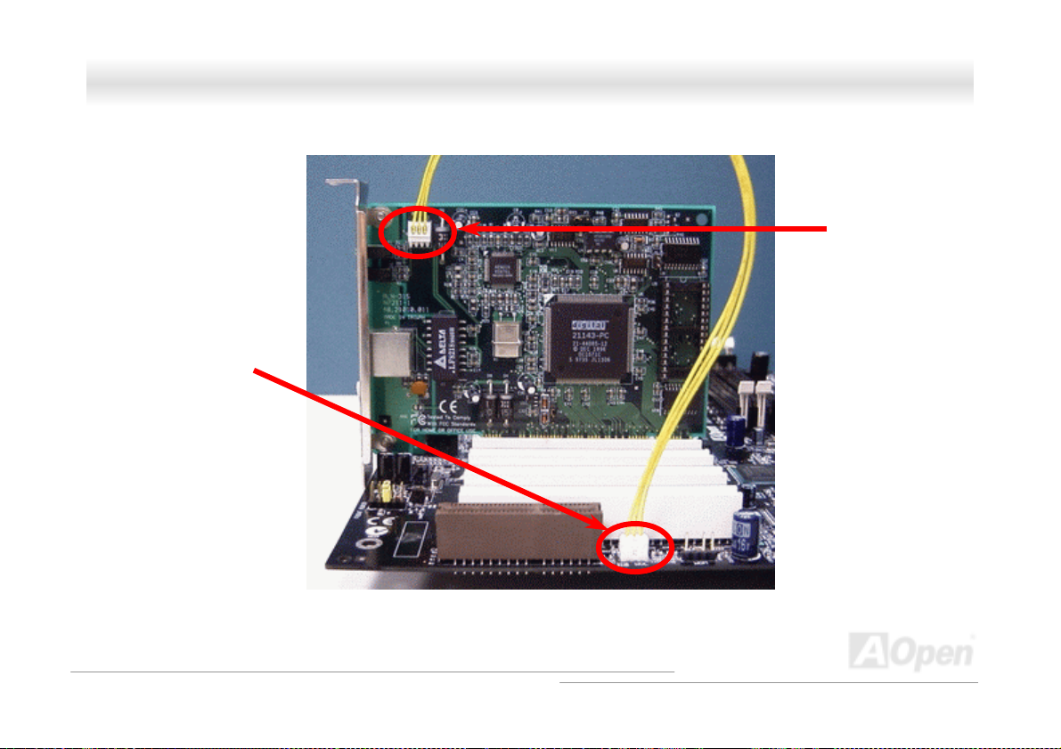
IrDA Connector ..............................................................................................................................................................39
WOM (Zero Voltage Wake on Modem) Connector.........................................................................................................40
WOL (Wake on LAN).....................................................................................................................................................43
CNR (Communication and Network Riser) Expansi on Slot ............................................................................................45
Support Intel
JP13 LAN Enable / Disable Select Jumper (Optional ) ...................................................................................................47
PC99 Color Coded Back Panel......................................................................................................................................48
COM2 Connector........................................................................................................................................................... 49
Support 2
DVO (Digital Video Out) Connector ...............................................................................................................................51
Chassis Intrusion Sensor...............................................................................................................................................52
CD Audio Connector......................................................................................................................................................53
Modem Audio Connector ...............................................................................................................................................54
®
PRO/100 Network Connection (Optional)................................................................................................ 46
nd
USB Port.....................................................................................................................................................50
OOnnlliinnee MMaannuuaall
3
Page 4

MMXX33WW--EE33 // MMXX33WW--VV33
AUX-IN Connector.........................................................................................................................................................55
Front Audio Connector...................................................................................................................................................56
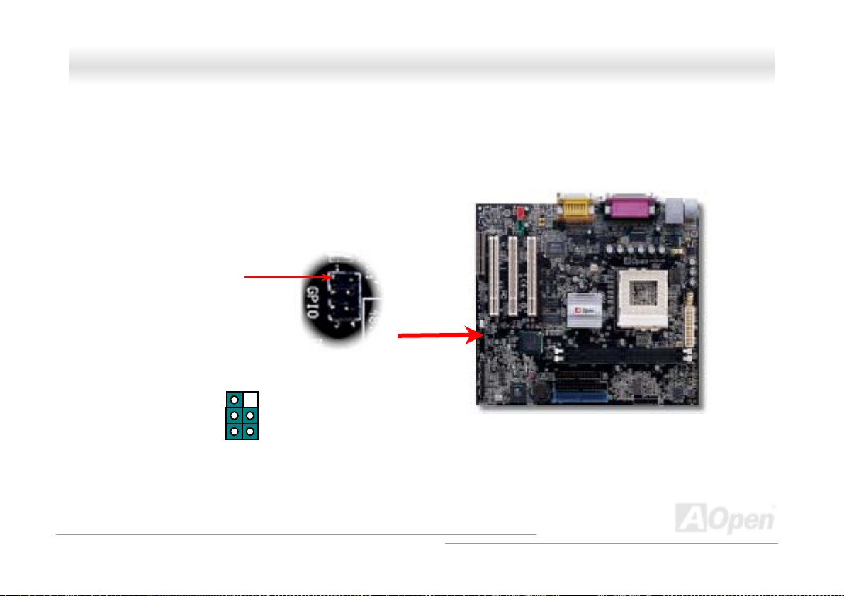
GPO (General Purpose Output) Connector ...................................................................................................................57
Over-current Protection .................................................................................................................................................59
Hardware Monitoring .....................................................................................................................................................60
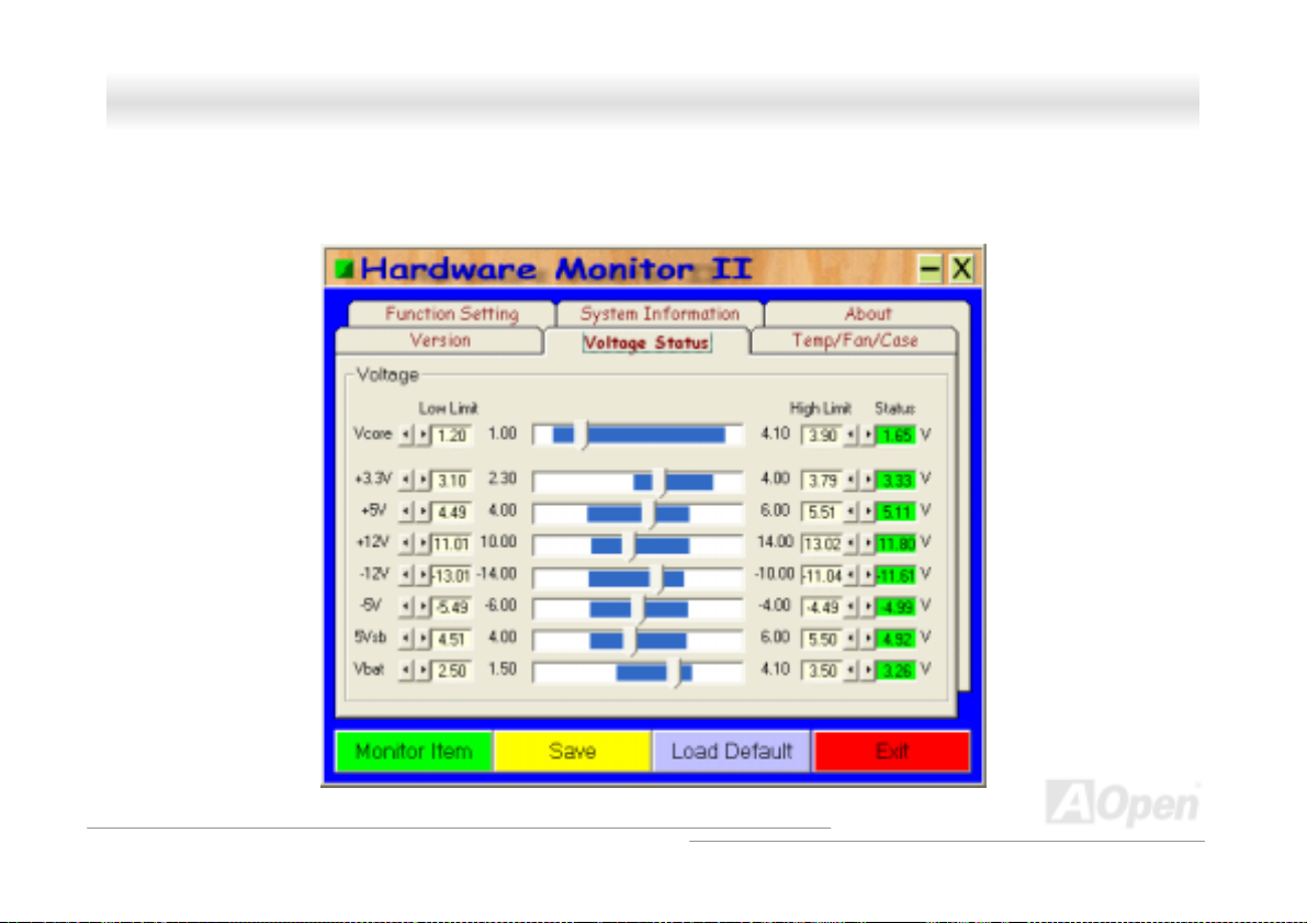
Resettable Fuse ............................................................................................................................................................61
Low ESR Capacitor .......................................................................................................................................................62
Layout (Frequency Isolation Wall) .................................................................................................................................64
Driver and Utility..........................................................................................................................65
Auto-run Menu from Bonus CD Disc .............................................................................................................................. 66
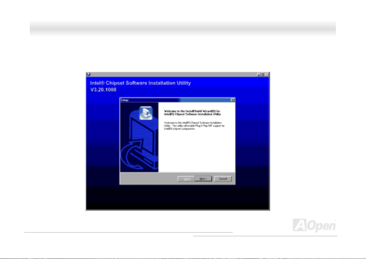
Installing Chipset Software I nstallatio n Utilit y ................................................................................................................ 67
Installing Onboard AGP Driver.......................................................................................................................................6 8
Installing Intel IAA Driver ...............................................................................................................................................69
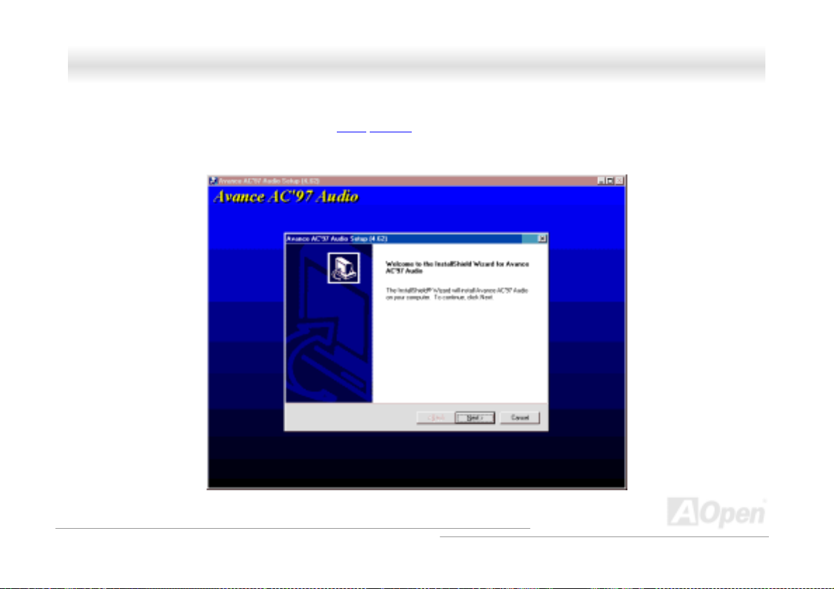
Installing Onboard Sound Driver....................................................................................................................................70
Installing LAN Driver (Optional) .....................................................................................................................................71
Installing Hardware Monitoring Uti lity ............................................................................................................................72
ACPI Suspend to Hard Drive......................................................................................................................................... 73
ACPI Suspend to RAM (STR)........................................................................................................................................77
AWARD BIOS ................................................................................................................................79
OOnnlliinnee MMaannuuaall
4
Page 5

MMXX33WW--EE33 // MMXX33WW--VV33
How To Use Award™ BIOS Setup Program...................................................................................................................80
How To Enter BIOS Setup .............................................................................................................................................81
BIOS Upgrade ...............................................................................................................................................................82
Overclocking ................................................................................................................................84
VGA Card & Hard Disk ..................................................................................................................................................85
Glossary .......................................................................................................................................8 6
AC97 .............................................................................................................................................................................86
ACPI (Advanced Configuratio n & Power Interfac e) ........................................................................................................86
AGP (Accelerated Graphic Port)....................................................................................................................................86
AMR (Audio/Modem Riser)............................................................................................................................................87
AOpen Bonus Pack CD .................................................................................................................................................87
APM (Advanced Power Management)........................................................................................................................... 87
ATA (AT Attachment)......................................................................................................................................................87
ATA/66...........................................................................................................................................................................87
ATA/100......................................................................................................................................................................... 88
BIOS (Basic Input/Output Sys tem) ................................................................................................................................ 88
Bus Master IDE (DMA mode).........................................................................................................................................88
CNR (Communication and Networki ng Riser)................................................................................................................88
CODEC (Coding and Decoding) ....................................................................................................................................89
OOnnlliinnee MMaannuuaall
5
Page 6

MMXX33WW--EE33 // MMXX33WW--VV33
DDR (Double Data Rated) SDRAM................................................................................................................................89
DIMM (Dual In Line Memory Module) ............................................................................................................................89
DMA (Direct Memory Access) ........................................................................................................................................ 89
ECC (Error Checking and Correction)............................................................................................................................90
EDO (Extended Data Output) Memory...........................................................................................................................90
EEPROM (Electronic Erasable Programmab le ROM)....................................................................................................90
EPROM (Erasable Programmabl e ROM).......................................................................................................................90
EV6 Bus ........................................................................................................................................................................91
FCC DoC (Declaration of Conformity)............................................................................................................................ 91
FC-PGA (Flip Chip-Pin Grid Array) ................................................................................................................................ 9 1
Flash ROM ....................................................................................................................................................................91
FSB (Front Side Bus) Clock ...........................................................................................................................................9 2
2
I
C Bus .......................................................................................................................................................................... 92
IEEE 1394 .....................................................................................................................................................................92
Parity Bit........................................................................................................................................................................93
PBSRAM (Pipelined Burst S RAM) .................................................................................................................................93
PC-100 DIMM ................................................................................................................................................................ 93
PC-133 DIMM ................................................................................................................................................................ 93
PC-1600 or PC-2100 DDR DRAM .................................................................................................................................93
OOnnlliinnee MMaannuuaall
6
Page 7

MMXX33WW--EE33 // MMXX33WW--VV33
PCI (Peripheral Component Interface) Bus.................................................................................................................... 9 4
PDF Format...................................................................................................................................................................94
PnP (Plug and Play) ......................................................................................................................................................94
POST (Power-On Self Test) ...........................................................................................................................................9 4
RDRAM (Rambus DRAM).............................................................................................................................................. 95
RIMM (Rambus Inline Memory Module)......................................................................................................................... 95
SDRAM (Synchronous DRAM) ......................................................................................................................................95
Shadow E
SIMM (Single In Li ne M emory Mod ule).......................................................................................................................... 96
SMBus (System Management Bus) ...............................................................................................................................96
SPD (Serial Presence Detect ) .......................................................................................................................................96
Ultra DMA ...................................................................................................................................................................... 97
USB (Universal Serial B us) ............................................................................................................................................ 9 7
VCM (Virtual Channel Memory).....................................................................................................................................98
ZIP file...........................................................................................................................................................................98
Troubleshooting........................................................................................................................... 9 9
Technical Support ......................................................................................................................103
Product Registration..................................................................................................................106
How to Contact Us.....................................................................................................................107
2
PROM ..........................................................................................................................................................95
OOnnlliinnee MMaannuuaall
7
Page 8

MMXX33WW--EE33 // MMXX33WW--VV33
OOnnlliinnee MMaannuuaall
YYoouu MMuusstt NNoottiiccee
Adobe, the Adobe logo, Acrobat is trademarks of Adobe Systems Incorporated.
AMD, the AMD logo, Athlon and Duron are trademarks of Advanced Micro Devices, Inc.
Intel, the Intel logo, Intel Celeron, Pentium II, Pentium III are trademarks of Intel Corporation.
Microsoft, Windows, and Windows logo are either registered trademarks or trademarks of Microsoft Corporation in the United
States and/or other countries.
All product and brand names used on this manual are used for identification purposes only and may be the registered
trademarks of their respective owners.
All of the specifications and information contained in this manual are subject to change without notice. AOpen reserves the right
to revise this publication and to make reasonable changes. AOpen assumes no responsibility for any errors or inaccuracies that
may appear in this manual, including the products and software described in it.
This documentation is protected by copyright law. All rights are reserved.
No part of this document may be used or reproduced in any form or by any means, or stored in a database or retrieval
system without prior written permission from AOpen Corporation.
Copyright
©
1996-2000, AOpen Inc. All Rights Reserved.
8
Page 9

MMXX33WW--EE33 // MMXX33WW--VV33
OOnnlliinnee MMaannuuaall
BBeeffoorree YYoouu SSttaarrtt
This Online Manual will introduce to the user how this product is installed. All useful information will be described in later
chapters. Please keep this manual carefully for future upgrades or system configuration changes. This Online Manual is saved
in PDF format
get free download from Adobe web site
Although this Online Manual is optimized for screen viewing, it is still capable for hardcopy printing, you can print it by A4 paper
size and set 2 pages per A4 sheet on your printer. To do so, choose File > Page Setup and follow the instruction of your printer
driver.
Thanks for the help of saving our earth.
, we recommend using Adobe Acrobat Reader 4.0 for online viewing, it is included in Bonus CD disc or you can
.
9
Page 10

MMXX33WW--EE33 // MMXX33WW--VV33
OOnnlliinnee MMaannuuaall
OOvveerrvviieeww
Thank you for choosing AOpen MX3W-E3 / MX3W-V3 motherboard. This motherboard is Intel® Socket 370 motherboard (M/B)
based on the microATX form featuring the Intel
performance chipset built in the M/B, this motherboard can support Intel
(including Coppermine and Tualatin) and 66/100/133MHz Front Side Bus (FSB)
on-board AGP function in 1X/2X mode and pipelined spilt-transaction long burst transfer up to 533MB/sec. According to
different customer’s requirements, SDRAM
motherboard and the maximum memory size can be up to 512MB. The
on-board IDE controller supports Ultra DMA
transfer rate up to 100MB/s. Further flexibility can be achieved by
taking advantage of the Communication and Network Riser (CNR)
option that allows audio and modem configuration on a single
baseboard design. Besides, this motherboard has an AC97
chipset onboard to provide high performance and amazing
surround stereo sound to let people enjoy working with it. Now,
welcom e to enjoy all feat ures f rom AOpe n MX3W-E3 / MX3W-V3
motherboard.
®
810E chipset (MX3W-E3) and Intel® 810 chipset (MX3W-V3). With a high
can be applied to this
33/66/100 mode and the
CODEC
®
Socket 370 series Pentium® III & Cel eron™ pr ocess or
clock. In the AGP performance, it supports
card
10
Page 11

MMXX33WW--EE33 // MMXX33WW--VV33
OOnnlliinnee MMaannuuaall
FFeeaattuurree HHiigghhlliigghhtt
CPU
Supports Intel® Socket 370 Pentium® III & Celeron™ 533MHz~1GHz+ with 66/100/133MHz FSB (Front Side Bus) designed for
Socket 370 technology.
Chipset
With the Intel® 810E chipset, Intel delivers a discrete graphics solution with all the performance, innovative features and proven
reliability of the Intel
AGP graphics solution for Intel
chipset's I/O Controller Hub (ICH2) features internal LAN capability and two USB controllers supporting four USB ports. With
support for six channels of AC97 audio and the ability to make the most of soft audio/modem technology, the 810E chipset
delivers an ideal solution for innovative new form factors. The Intel® 810 chipset consists of a Graphics and Memory Controller
Hub (GMCH) Host Bridge and an I/O Controller Hub (ICH/ICH0) Bridge for the I/O subsystem. The GMCH integrates a system
memory DRAM controller that supports a 64-bit 100 MHz DRAM array.
®
i810E2 chipset family. With its highly scalable design, the new 810E chipset offers an ideal, leading-edge
®
Pentium® III / Celeron™ processor platforms. And the smart integration in the Intel 810E
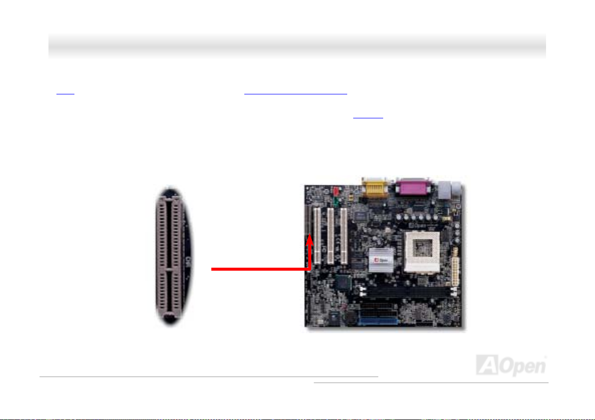
Expansion Slots
Including three 32-bit/33MHz PCI and one CNR expansion slots. The PCI local bus throughput can be up to 132MB/s. The
Communication & Nectworking Riser (CNR)
Modem/LAN/Audio card.
slot provided by MX3W-E3 / MX3W-V3 can support CNR interface for a
11
Page 12

MMXX33WW--EE33 // MMXX33WW--VV33
OOnnlliinnee MMaannuuaall
Memory
This motherboard provides two 168-pin SDRAM DIMM socket that support up to 512MB of PC-100 or PC-133 compliant SDRAM
(Synchronous Dynamic Random Access Memory). You may install 32, 64, 128, 256 and 512MB with Non-ECC SDRAM modules.
Ultra DMA 33/66/100 Bus Mater IDE
Comes with an on-board PCI Bus Master IDE controller with two connectors that supports four IDE devices in two channels,
supports Ultra DMA
33/66/100, PIO Modes 3 and 4 and Bus Master IDE DMA Mode 4, and supports Enhanced IDE devices.
On-board AC97 Sound
MX3W-E3 / MX3W-V3 is equipped with Realtek ALC201 sound chip. This on-board audio includes a complete audio recording
and playback system.
Power Management/Plug and Play
The MX3W-E3 / MX3W-V3 supports the power management function that confirms to the power-saving standards of the U.S.
Environmental Protection Agency (EPA) Energy Star program. It also offers Plug-and-Play
configuration problems, thus making to system user-friendlier.
, which helps save users from
Hardware Monitoring Management
Supports CPU or system fans status, temperature and voltage monitoring and alert, through the on-board hardware monitor
module and AOpen Hardware Monitoring Utility
.
12
Page 13

MMXX33WW--EE33 // MMXX33WW--VV33
Enhanced ACPI
Fully implement the ACPI standard for Windows® 95/98/ME/NT/2000 series compatibility, and supports Soft-Off, STR (Suspend
to RAM, S3), STD (Suspend to Disk, S4), WOM (Wake On Modem), WOL (Wake On LAN) features.
Super Multi-I/O
MX3W-E3 / MX3W-V3 provides two high-speed UART compatible serial ports and one parallel port with EPP and ECP
capabilities. UART2 can also be directed from COM2 to the Infrared Module for the wireless connections.
OOnnlliinnee MMaannuuaall
13
Page 14

MMXX33WW--EE33 // MMXX33WW--VV33
OOnnlliinnee MMaannuuaall
QQuuiicckk IInnssttaallllaattiioonn PPrroocceedduurree
This page gives you a quick procedure on how to install your system. Follow each step accordingly.
1.
Installing CPU and Fan
2.
Installing System Memory (DIMM
3.
Connecting Front Panel Cable
4.
Connecting IDE and Floppy Cable
5.
Connecting ATX Power Cable
6.
Connecting Back Panel Cable
7.
Power-on and Load BIOS Setup Default
8.
Setting CPU Frequency
9.
Reboot
10.
Install in g Op erat i ng Sy st em (s uc h as W ind ows 98 )
11.
Installing Driver and Utility
14
Page 15
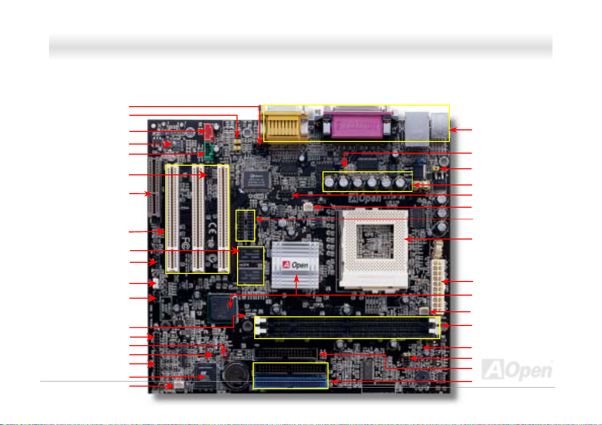
A
r
r
A
MMXX33WW--EE33 // MMXX33WW--VV33
CD-IN Connecto
Front Audio Connector
MODEM-CN Connector
Onboard AC97 CODEC Chip
AUX-IN Connecto
IrDA Connector
CNR Expansion Slot
32-bit PCI Expansion Slot x3
4MB Display Cache
WOM (Wake on Modem)
WOL (Wake on LAN)
GPO Connector
System Power LED
nd
2
USB Port Connector
JP14 CMOS Clear Jumper
Chassis Open Intruder
Front Panel Connector
4Mbit Flash ROM BIOS
Motherboard Map
Here we use MX3W-E3 motherboard as illustration.
15
OOnnlliinnee MMaannuuaall
PC99 Colored Back Panel
JP13 LAN Enable/Disable Select
Jumper (Optional)
JP28 Keyboard/M
Enable/Disable Jumper
Low ESR Condensers
COM2 Port Connector
Fan3 Connector
DVO Connector
370-pin CPU So
Frequency/Voltage Auto-detection
that supports Intel® Pentium® III and
Celeron™ Processors (including
Coppermine and Tualatin)
533MHz~1GHz+ CPU
TX Power Connector
Intel® 810E Chipset for MX3W-E3
®
Or Intel
CPU Fan Connector
168-pin DIMM Sock
maximum memory size up to
512MB
RAM Power LED
JP23 FSB Select Jumper
FDD Connector
TA/100 IDE Connector x2
cket with
810 Chipset for MX3W-V3
ouse Wake-up
et x2 supports
Page 16
MMXX33WW--EE33 // MMXX33WW--VV33
OOnnlliinnee MMaannuuaall
BBlloocckk DDiiaaggrraamm
PCI Card
44xxUUSSBB
CNR Card
MIC, Line-in
and Speaker
Graphics Memory
Control Hub
Hub Link
PPCCII BBuuss
AC97 Link
Audio
CODEC
CPU
66/100/133MHz
(GMCH)
I/O Control
Hub (ICH2)
Low Pin
Count
Super
100MHz
Mem o r y B us
ATA
33/66/100
IDE Bus
LPC
I/O
Clock Generator
IMM
DDI
HDD/CDROM
4Mb BIOS ROM
Floppy
Serial port, Printer
and PS/2 KB/Mouse
16
Page 17

MMXX33WW--EE33 // MMXX33WW--VV33
OOnnlliinnee MMaannuuaall
HHaarrddwwaarree IInnssttaallllaattiioonn
This chapter describes jumpers, connectors and hardware devices of this motherboard.
Note: El ectrostatic discharge (ESD) can damage your processor, disk drives, expansion boards, and
other components. Always read the following precautions before you install a system component.
1. Do not remove a component from its protective packaging until you are ready to install it.
2. Wear a wrist ground strap and attach it to a metal part of the system unit before handling a
component. If a wrist strap is not available, maintain contact with the system unit t hroughout any
procedure requiring ESD protection.
17
Page 18

MMXX33WW--EE33 // MMXX33WW--VV33
OOnnlliinnee MMaannuuaall
AAbboouutt ““OOppttiioonnaall”” aanndd ““UUppggrraaddee OOppttiioonnaall””……
When you read this online manual and start to assemble your computer system, you may find some of functions are “Optional”,
and some are “Upgrade Optional”. This is because all of AOpen motherboards include many amazing and powerful features;
however, some of these are not frequently used on daily operation. Therefore, we define some key features as optional to meet
different requirements. Functions that can be upgraded by users are defined as “Upgrade Optional”. The other optional functions
which may have been built on the motherboards and which you cannot upgrade by yourself, we call them “Optional”. If needed,
you can contact your local distributors or resellers to purchase “Upgrade Optional” components. Also you can visit AOpen official
web site: www.aopen.com.tw
to get detailed information.
18
Page 19

(
MMXX33WW--EE33 // MMXX33WW--VV33
OOnnlliinnee MMaannuuaall
Default)
1
Clear CMOS
Tip: W hen should I Clear CMOS?
1. Boot fa il bec aus e of ov e rcl ock in g…
2. Forget password…
3. Troubleshooting…
CClleeaarr CCMMOOSS DDaattaa
You can clear CMOS to restore system default setting. To clear the CMOS, follow the procedure below.
1. Turn off the system and unplug the AC power.
2. Remove ATX power cable from connector PWR2.
3. Locate JP14 and short pins 2-3 for a few seconds.
4. Return JP14 to its normal setting by shorting pin1 & pin2.
5. Connect ATX power cable back to connector PWR2.
Pin 1
1
Normal Operation
19
Page 20
MMXX33WW--EE33 // MMXX33WW--VV33
OOnnlliinnee MMaannuuaall
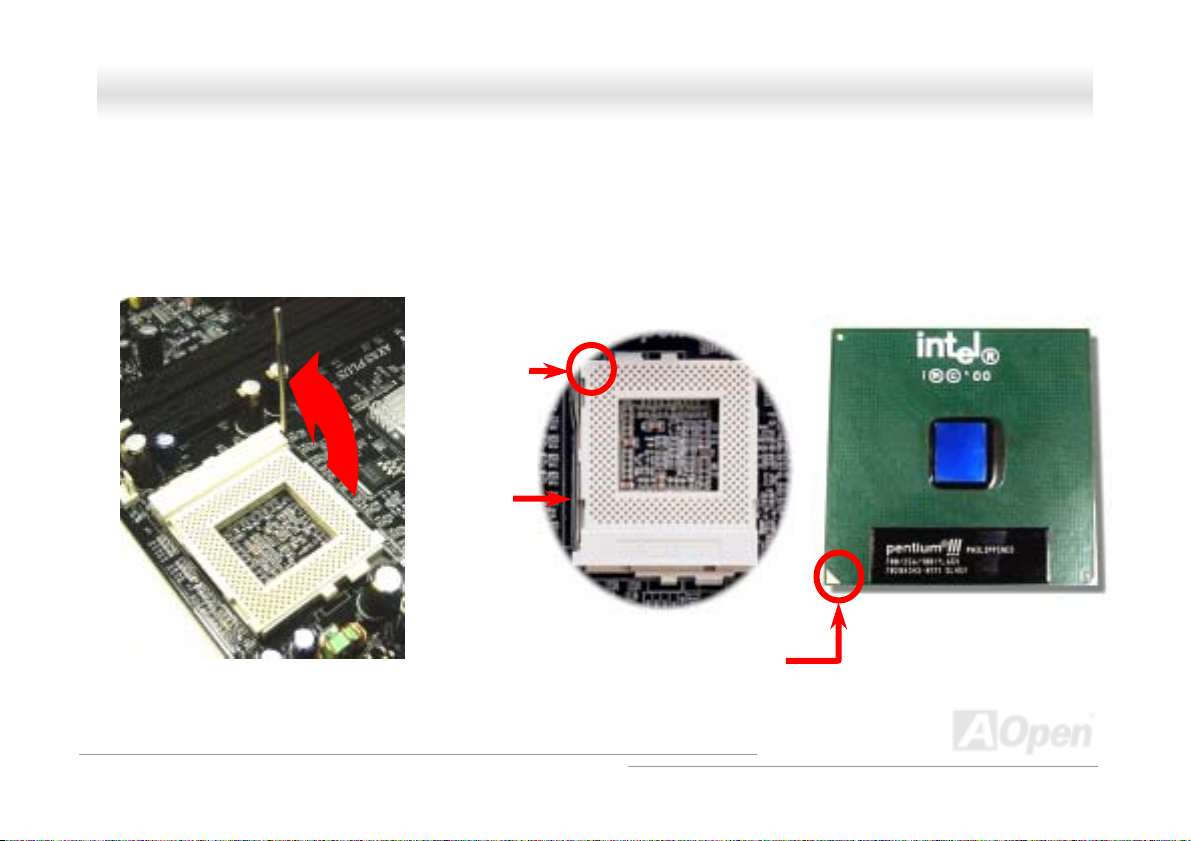
CCPPUU IInnssttaallllaattiioonn
This motherboard supports Intel® Pentium III and Celeron Socket370 CPU. Beware of CPU orientation when you plug it into
CPU socket. To finish CPU installation, please follow the procedure as shown below:
1. Pull up CPU socket lever up to
90-degree angle.
2. Locate the position of Pin 1. You will find “CPU PIN1” marked at the
upper left of the socket on the motherboard. Aim CPU cut edge at Pin 1
position and insert CPU into the socket.
CPU pin 1
and cut edge
N.B. These pictures are for reference only. They may slightly look different from the product you purchase.
CPU socket
Lever
CPU cut edge
20
Page 21

g
MMXX33WW--EE33 // MMXX33WW--VV33
3. Press down the CPU socket lever to finish
CPU installation.
N.B. These pictures are for reference only. They may slightly look different from the product you purchase.
CPU cut edge
Note: If you do not insert CPU well or
go wrong with its direction, you may
dama
e the CPU.
OOnnlliinnee MMaannuuaall
21
Page 22
(
MMXX33WW--EE33 // MMXX33WW--VV33
OOnnlliinnee MMaannuuaall
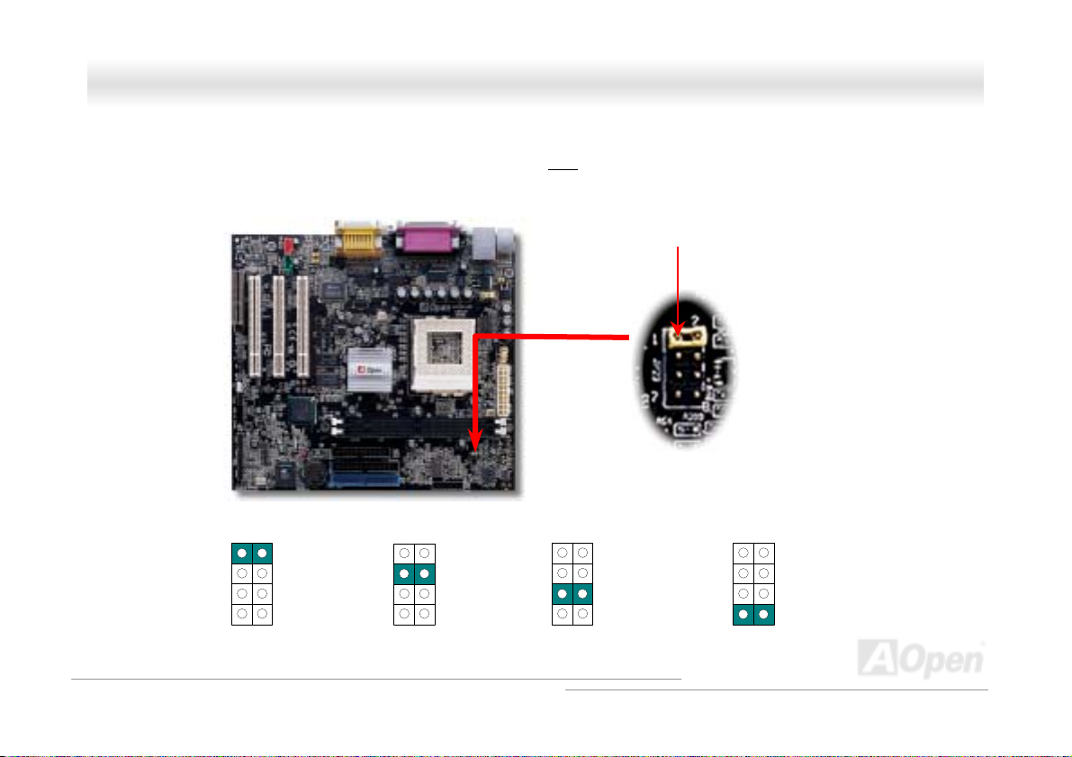
JJPP2233 AAddjjuusstt FFSSBB//PPCCII CClloocckk RRaattiioo
This jumper is used to specify the relationship between PCI and FSB clock. Generally speaking, if you are not an overclocker,
we don’t recommend you to change the default setting.
Pin1
1
Auto
Default)
1 1 1
FSB=133MHz
FSB=100MHz
22
FSB=66MHz
Page 23

MMXX33WW--EE33 // MMXX33WW--VV33
PCI Clock = CPU FSB Clock / Clock Ratio
AGP Clock = PCI Clock x 2
Clock Ra tio CPU (Host) PCI AGP Memory
2X 66MHz 33MHz 66 PCI x2 or x3
2X, overclocking 75MHz 37.5MHz 75MHz PCI x2 or x3
3X 100MHz 33MHz 66MHz PCI x2 or x3 or x4
3X, overclocking 112MHz 37.3MHz 74.6MHz PCI x2 or x3 o r x4
4X 133MHz 33MHz 66MHz PCI x3 or x4
4X, overclocking 155MHz 38.75MHz 77.5MHz PCI x3 or x4
Warning: Intel® 810E chipset supports maximum 133MHz FSB
and 810 chipset supports maximum 100MHz FSB. Both support
66MHz AGP clock. Higher clock setting may cause serious
system damage.
OOnnlliinnee MMaannuuaall
23
Page 24

MMXX33WW--EE33 // MMXX33WW--VV33
OOnnlliinnee MMaannuuaall
CCPPUU JJuummppeerr--lleessss DDeessiiggnn
CPU VID signal and SMbus clock generator provide CPU voltage auto-detection and allow the user to set CPU frequency
through BIOS setup
designs are eliminated. There will be no worry of wrong CPU voltage detection anymore.
; therefore, no jumpers or switches are used. The disadvantages of original Pentium based jumper-less
Intel® Socket 370
Pentium III &
Celeron CPU
CPU VID signal
Power Regulator
(A utomatically generates CPU voltage)
CPU Freq. Ratio
CPU voltage
Clock
Generator
BIOS
Controlled
Circuit
24
Page 25

MMXX33WW--EE33 // MMXX33WW--VV33
OOnnlliinnee MMaannuuaall
SSeettttiinngg CCPPUU CCoorree VVoollttaaggee
This motherboard supports CPU VID function. The CPU core voltage will be automatically detected and the range is from 1.3V
to 2.0V. It is no need to set CPU Core Voltage.
25
Page 26
MMXX33WW--EE33 // MMXX33WW--VV33
SSeettttiinngg CCPPUU FFrreeqquueennccy
This motherboard is CPU jumper-less design; you can set CPU frequency in the BIOS setup. No jumpers or switches are
needed.
BIOS Setup > Frequency/Voltage Control > CPU Speed Setting
CPU Ratio
CPU FS B
Warning: Intel® 810E chipset supports maximum
133MHz FSB and 810 chipset supports maximum
100MHz FSB. Both support 66MHz AGP clock.
Higher clock setting may cause serious system
y
1.5x, 2x, 2.5x, 3x, 3.5x, 4x, 4.5x, 5x, 5.5x, 6x, 6.5x, 7x, 7.5x, and 8x
66~133MHz
Tip: If your system hangs or fails to boot
Home
because of overclocking, simply use <Home>
key to restore the default setting
OOnnlliinnee MMaannuuaall
26
Page 27
MMXX33WW--EE33 // MMXX33WW--VV33
OOnnlliinnee MMaannuuaall
SSuuppppoorrtteedd CCPPUU FFrreeqquueennccyy
Core Frequency = CPU Bus Clock * CP U Ra tio
PCI Clock = CPU Bus Clock / Clock Ratio
AGP Clock = PCI Clock x 2
CPU CPU Core Frequency FSB Clock Ratio
Celeron 533 533MHz 66MHz 8x
Celeron 566 566MHz 66MHz 8.5x
Celeron 600 600MHz 66MHz 9x
Celeron 667 667MHz 66MHz 10x
Celeron 700 700MHz 66MHz 10.5
Celeron 766 766MHz 66MHz 11.5x
Celeron 800 800MHz 100MHz 8x
Celeron 900 900MHz 100MHz 9x
Celeron 1G 1GHz 100MHz 10x
Celeron 1.1G 1.1GHz 100MHz 11x
Celeron 1.2G 1.2GHz 100MHz 12x
Pentium III 800E 800MHz 100MHz 8x
Pentium III 850E 850MHz 100MHz 8.5x
Note: This motherboard supports CPU
auto-detection function. Therefore, you
don’t need to set CPU frequency by
manual.
27
Page 28
A
MMXX33WW--EE33 // MMXX33WW--VV33
Pentium III 533EB 533MHz 133MHz 4x
Pentium III 600EB 600MHz 133MHz 4.5x
Pentium III 667EB 667MHz 133MHz 5x
Pentium III 733EB 733MHz 133MHz 5.5
Pentium III 800EB 800MHz 133MHz 6x
Pentium III 866EB 866MHz 133MHz 6.5
Pentium III 933EB 933MHz 133MHz 7x
Pentium III 1000EB 1GHz 133MHz 7.5x
Pentium III 1G 1GHz 133MHz 7.5x
Pentium III 1.13G 1.13GHz 133MHz 8.5 x
Pentium III 1.2G 1.2GHz 133MHz 9x
Pentium III 1.3G 1.3GHz 133MHz 10x
Warning: Intel® 810E chipset supports maximum 133MHz FSB and
810 chipset supports maximum 100MHz FSB. Both support 66MHz
GP clock. Higher clock setting may cause serious system damage.
OOnnlliinnee MMaannuuaall
28
Page 29
MMXX33WW--EE33 // MMXX33WW--VV33
OOnnlliinnee MMaannuuaall
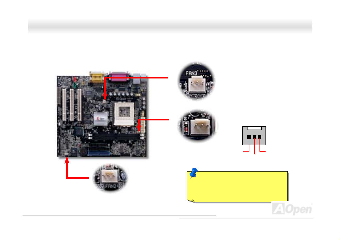
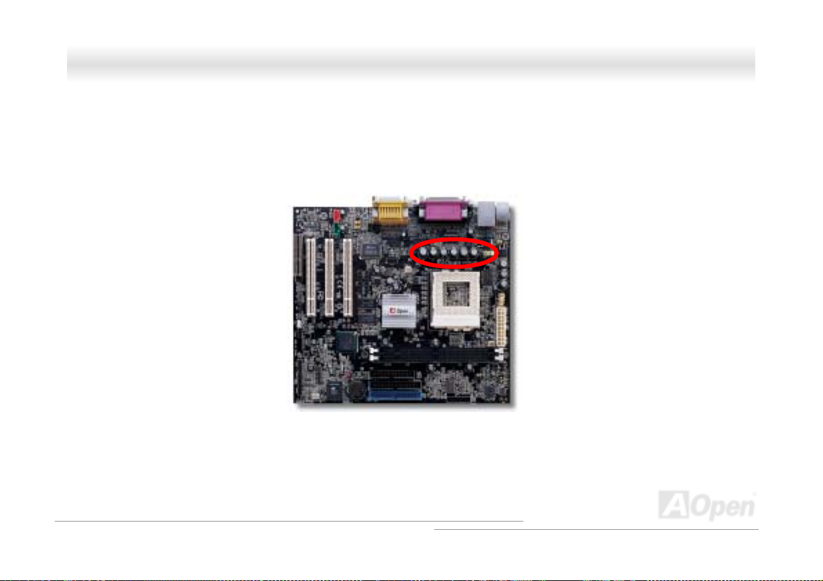
CCPPUU aanndd HHoouussiinngg FFaann CCoonnnneeccttoorr ((wwiitthh HH//WW MMoonniittoorriinngg))
Plug in t he CPU fan c able to the 3 -pin CPU FAN connector. If you have chassis fan, you can also plug it on FAN2 or FAN3
connector.
FAN2 Connector
Note: Some CPU fans do not have
sensor pin, so they cannot support fan
monitoring.
FAN3 Connector
CPU Fan Connector
SENSOR
GND
+12V
29
Page 30

MMXX33WW--EE33 // MMXX33WW--VV33
OOnnlliinnee MMaannuuaall
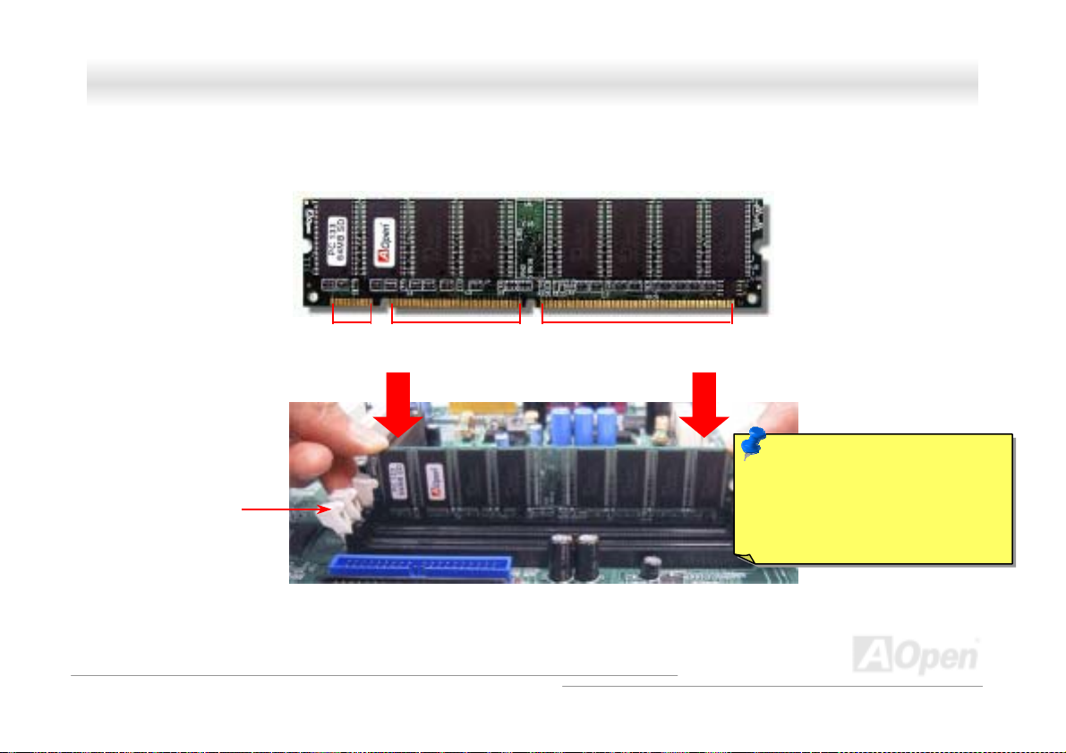
DDIIMMMM SSoocckkeett
This motherboard has two 168-pin DIMM sockets that allow you to install PC100 or PC133 memory up to 512MB. It also
supports SDRAM Modules.
DIMM1
DIMM2
30
Page 31
MMXX33WW--EE33 // MMXX33WW--VV33
OOnnlliinnee MMaannuuaall
HHooww ttoo IInnssttaallll MMeemmoorryy MMoodduulleess
Please follow the procedure as shown to install memory.
1. Make sure to put the module pins face down and match the socket’s size as depicted below.
2. Insert the module straight down to the DIMM slot with both hands and press firmly until the DIMM module is securely in
place.
3. Repeat step 2 to install the other DIMM modules.
N.B. These pictures are for reference only. They may slightly look different from the product you purchase.
Tab
20 pins 60 pins 88 pins
Note: The tabs of the DIM M slot
will close-up and hold the
memory module in place when
the module has been firmly
located.
31
Page 32
e
V
V
V
MMXX33WW--EE33 // MMXX33WW--VV33
OOnnlliinnee MMaannuuaall
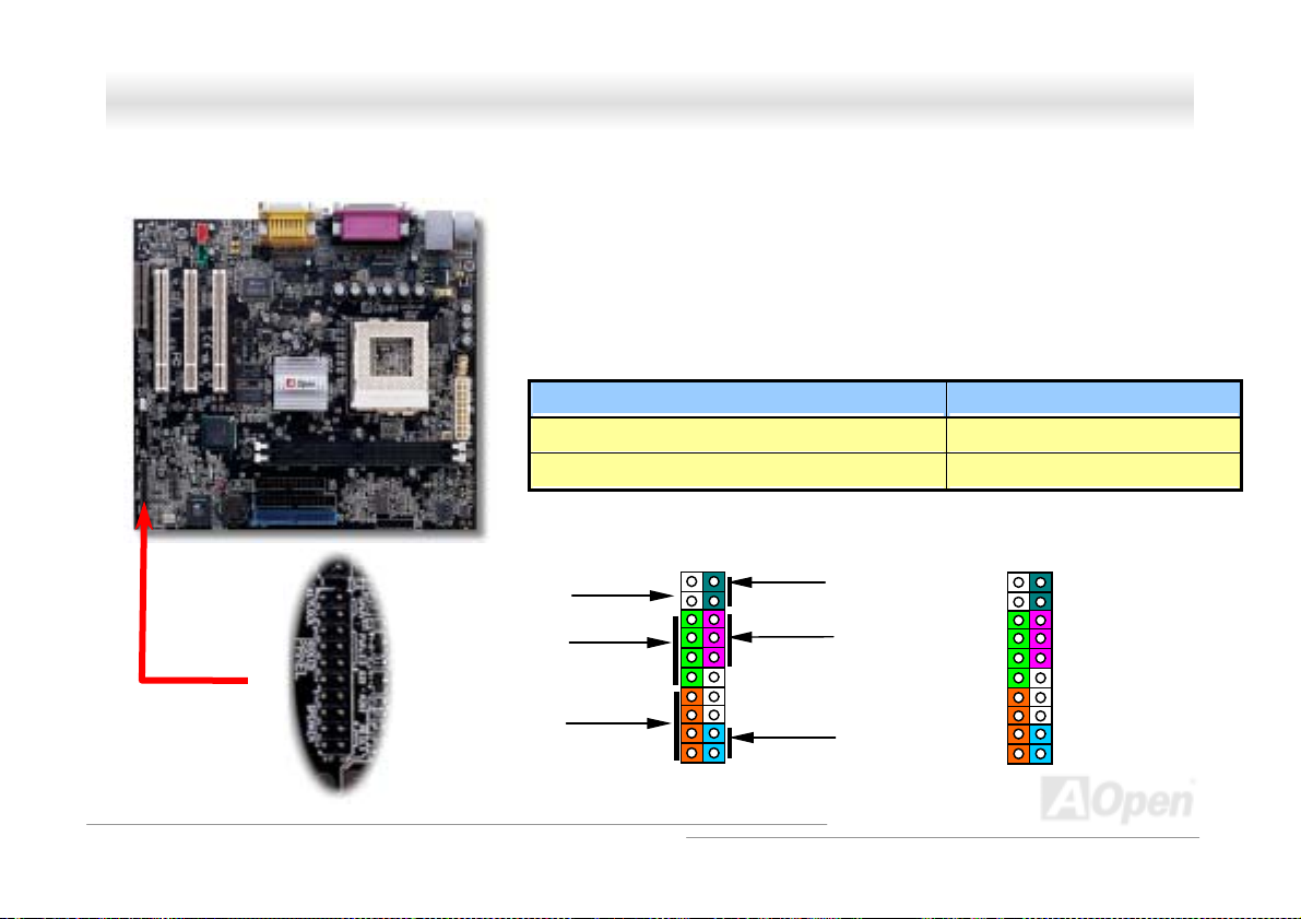
FFrroonntt PPaanneell CCoonnnneeccttoorr
Attach the power LED, EMPI, speaker, power and reset switch connectors to th
corresponding pins. If you enable “Suspend Mode” item in BIOS Setup, the ACPI
& Power LED will keep flashing while the system is in suspend mode.
Locate the power switch cable from your ATX housing. It is 2-pin female
connector from the housing front panel. Plug this connector to the soft-power
switch connector marked SPWR.
Suspend Type ACPI L E D
Power on Suspend (S1) Flashing for every second
Suspend to RAM (S3) or Suspend to Disk (S4) The LED will be turned off
GND
+5
IDE LED
IDE LED
+5
+5
GND
NC
1
5VSB
PWRBTI
ACPILED GND
ACPILED
NC
NC
GND
RESET
GND
IDE LED
SPEAKER
1
-
+
+
SPWR
ACPI &
+
POWER LED
+
RESET
Keylock-
SPEAKER
32
Page 33

MMXX33WW--EE33 // MMXX33WW--VV33
OOnnlliinnee MMaannuuaall
AATTXX PPoowweerr CCoonnnneeccttoorr
The ATX power supply uses 20-pin connector shown below. Make sure you plug in the right direction.
+12V
5VSB
PW-OK
COM
+5V
COM
+5V
COM
+3.3V
+3.3V
+5V
+5V
-5V
COM
COM
COM
PS-ON
COM
-12V
+3.3V
33
Page 34

MMXX33WW--EE33 // MMXX33WW--VV33
OOnnlliinnee MMaannuuaall
JJPP2288 KKeeyybbooaarrdd//MMoouussee WWaakkee--uupp
This motherboard provides keyboard/mouse wake-up function. You can use the JP28 to enable or disable this function.
Please note that both USB and PS/2 types of keyboard and mouse are supported in this function.
JP28
KB/Mouse Wake-up
Pin1
1
Disable
(Default)
1
Enable
34
Page 35

MMXX33WW--EE33 // MMXX33WW--VV33
OOnnlliinnee MMaannuuaall
PPoowweerr aanndd RRAAMM PPoowweerr IInnddiiccaattee LLEEDD
These two LED indicate if power is supplied to motherboard and memory properly. You can easily check the status of power
supply when the system is powered on or when the system is under Suspend to RAM
mode.
RAM Powe r
LED
Warning: Do not install or remove the
DIMM module when the RAM power LED
is on.
System
Power LED
35
Page 36

MMXX33WW--EE33 // MMXX33WW--VV33
OOnnlliinnee MMaannuuaall
AACC PPoowweerr AAuuttoo RReeccoovveerryy
A traditional ATX system remains power off when AC power resumes from power failure. This design is inconvenient for a
network server or workstation, without an UPS, that needs to stay power-on. To solve this problem, this motherboard
implements an AC Power Auto Recovery function.
36
Page 37

MMXX33WW--EE33 // MMXX33WW--VV33
OOnnlliinnee MMaannuuaall
Pin 1
ATA 33/66/100 IDE
Connector
Pin 1
FDD Connector
Secondary
Slave (4th)
Primary Slave
(2nd)
Secondary
Master (3rd)
Primary
Master (1st)
IIDDEE aanndd FFllooppppyy CCoonnnneeccttoorr
Connect 34-pin floppy cable and 40-pin IDE cable to FDD floppy connector and IDE connector. For clear identification, the blue
connector is IDE1. Be careful of the pin1 orientation. Wrong orientation may cause system damage.
37
Page 38

MMXX33WW--EE33 // MMXX33WW--VV33
IDE1 is also known as a primary channel and IDE2 as s econdary channel. Each channel supports two I DE devices that make a
total of four devices. In order to work together, the two devices on each channel must be set differently to Master and Slave
mode. Either one can be the hard disk or the CDROM. The setting as master or slave mode depends on the jumper on your IDE
device, so please refer to your hard disk and CDROM manual accordingly.
This motherboard supports ATA33
modes. The IDE bus is 16-bit, which means every transfer is two bytes.
Mode Clock Period Clock
PIO mode 0 30ns 20 600ns (1/600ns) x 2byte = 3.3MB/s
PIO mode 1 30ns 13 383ns (1/383ns) x 2byte = 5.2MB/s
PIO mode 2 30ns 8 240ns (1/240ns) x 2byte = 8.3MB/s
PIO mode 3 30ns 6 180ns (1/180ns) x 2byte = 11.1MB/s
PIO mode 4 30ns 4 120ns (1/120ns) x 2byte = 16.6MB/s
DMA mode 0 30ns 16 480ns (1/480ns) x 2byte = 4.16MB/s
DMA mode 1 30ns 5 150ns (1/150ns) x 2byte = 13.3MB/s
DMA mode 2 30ns 4 120ns (1/120ns) x 2byte = 16.6MB/s
UDMA 33 30ns 4 120ns (1/120ns) x 2byte x2 = 33MB/s
UDMA 66 30ns 2 60ns (1/60ns) x 2byte x2 = 66MB/s
UDMA100 20ns 2 40ns (1/40ns) x 2byte x2 = 100MB/s
Warning: Th e specif icati on of the I DE cable is a maximu m of 46cm
(18 inches); make sure your cable does not exceed this length.
, ATA66 or ATA100 IDE devices. Following table lists the transfer rate of IDE PIO and DMA
Count
Cycle Time Data Transfer Rate
38
OOnnlliinnee MMaannuuaall
Tip:
1. For better signal quality,
it is recommended to set
the far end side device
to master mode and
follow the suggested
sequence to install your
new device. Please refer
to above diagra m
2. To achieve the best
performance of Ultra
DMA 66/100 hard disks,
a special 80-wires IDE
cable for Ultra DMA
1 i r
ir
.
Page 39
r
X
MMXX33WW--EE33 // MMXX33WW--VV33
OOnnlliinnee MMaannuuaall
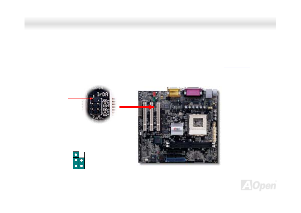
IIrrDDAA CCoonnnneeccttoorr
The IrDA connector can be configured to support wireless infrared module, with this module and application software such as
Laplink or Windows 95 Direct Cable Connection, the user can transfer files to or from laptops, notebooks, PDA devices and
printers. This connector supports HPSIR (115.2Kbps, 2 meters) and ASK-IR (56Kbps).
Install the infrared module onto the IrDA connector and enable the infrared function from BIOS Setup, UART2 Mode
to have the correct orientation when you plug in the IrDA connector.
Pin 1
NC
+5V GND
IR_T IR_RX
, make sure
IrDA Connecto
39
Page 40
MMXX33WW--EE33 // MMXX33WW--VV33
OOnnlliinnee MMaannuuaall
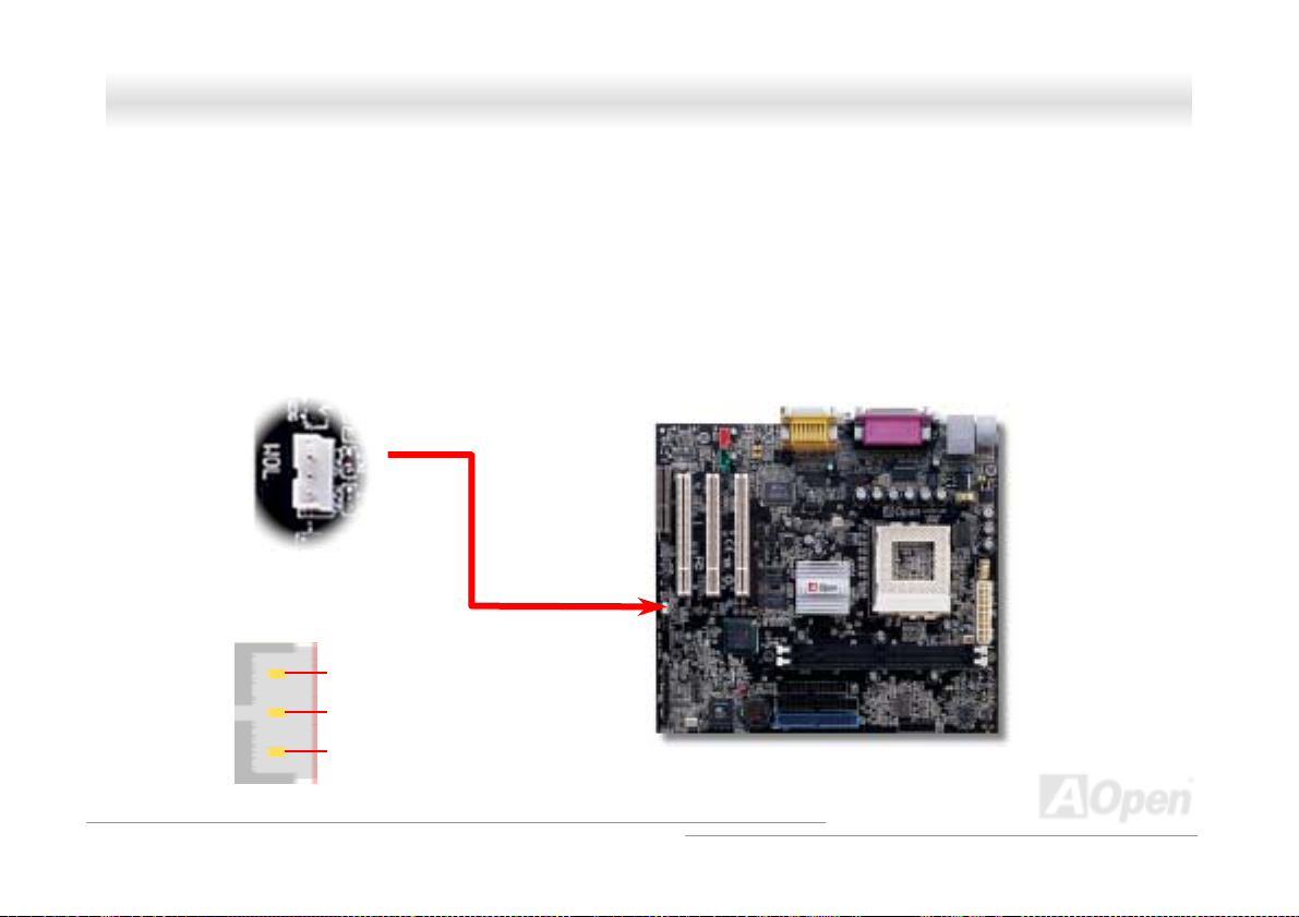
WWOOMM ((ZZeerroo VVoollttaaggee WWaakkee oonn MMooddeemm)) CCoonnnneeccttoorr
This motherboard implements special circuit to support Wake On Modem, both Internal modem card and external box modem
are supported. Since Internal modem card consumes no power when system power is off, it is recommended to use an internal
modem. To use internal modem, connect 4-pin cable from RING connector of modem card to the WOM connector on the
motherboard.
WOM Connector
+5VSB
NC
RI-
GND
40
Page 41
MMXX33WW--EE33 // MMXX33WW--VV33
WWOOMM bbyy EExxtteerrnnaall BBOOXX MMooddeem
Traditional Green PC suspend mode does not really turn off the system power supply, it uses external box modem to trigger MB
COM port and resume back to active.
N.B. This picture is for reference only. They may slightly look different from the product you purchase.
m
Pin 1
OOnnlliinnee MMaannuuaall
Serial Port
(Modem Side)
Serial Port
(Motherboard Side)
41
Page 42
MMXX33WW--EE33 // MMXX33WW--VV33
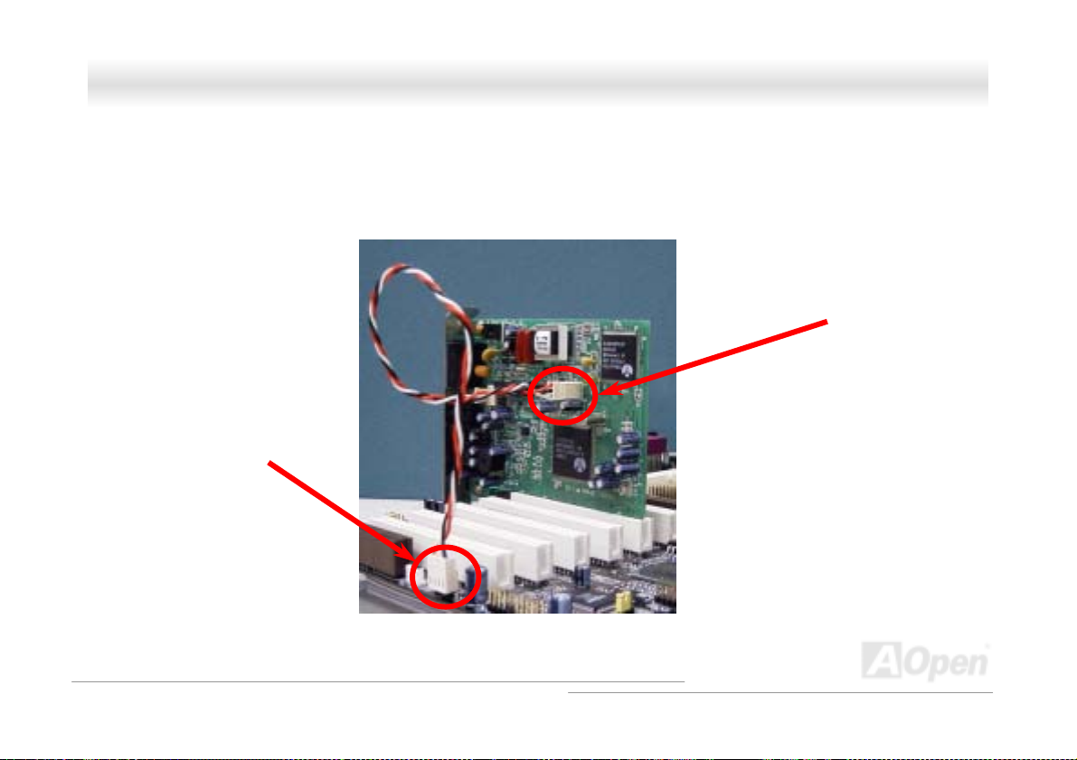
WWOOMM bbyy IInntteerrnnaall MMooddeemm CCaarrd
With the help of the ATX soft power On/Off, it is possible to have a system totally power off, and wakeup to automatically answer
a phone call as an answering machine or to send/receive a fax. You may identify whether or not your system is in true power off
mode by checking to see if the fan of your power supply is off. Both an external box modem and an internal modem card can be
used to support Modem Wake Up, but if you use an external modem, you have to leave your box modem on.
N.B. This picture is for reference only. They may slightly look different from the product you purchase.
WOM Connector
(Motherboard Side)
d
OOnnlliinnee MMaannuuaall
WOM Connector
(Modem Card Side)
42
Page 43
MMXX33WW--EE33 // MMXX33WW--VV33
OOnnlliinnee MMaannuuaall
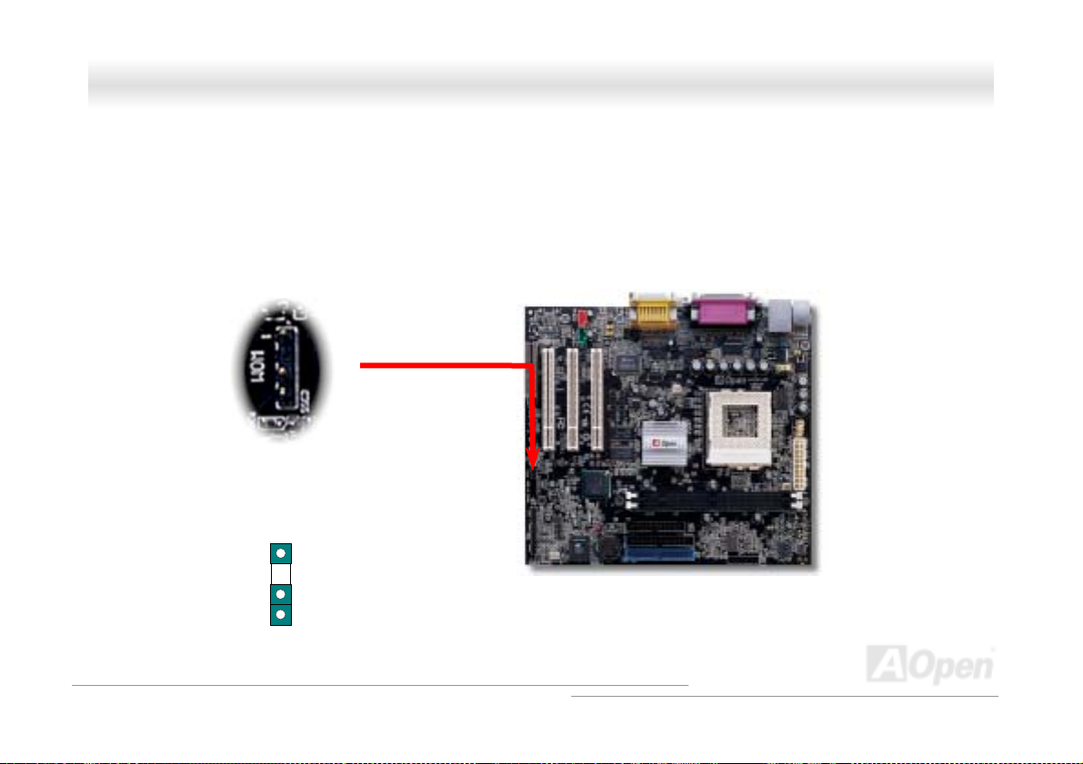
WWOOLL ((WWaakkee oonn LLAANN))
This feature is very similar as Wake On Modem, but it goes through local area network. To use Wake On LAN function, you must
have a network card with chipset that supports this feature, and connect a cable from LAN card to motherboard WOL connector.
The system identification information (probably IP address) is stored on network card and because there is a lot of traffic on the
Ethernet, you need to install network management software, such as ADM, for the checking of how to wake up the system. Note
that, at least 600mA ATX standby current is required to support the LAN card for this function.
LID
GND
+5VSB
43
Page 44
MMXX33WW--EE33 // MMXX33WW--VV33
OOnnlliinnee MMaannuuaall
WOL Connector
(Motherboard Side)
N.B. This picture is for reference only. They may slightly look different from the product you purchase.
WOL Connector
(Ethernet Card Side)
44
Page 45
MMXX33WW--EE33 // MMXX33WW--VV33
OOnnlliinnee MMaannuuaall
CCNNRR ((CCoommmmuunniiccaattiioonn aanndd NNeettwwoorrkk RRiisseerr)) EExxppaannssiioonn SSlloott
CNR is a riser card specification to replace the AMR (Audio/Modem Riser) that supports V.90 analog modem, multi-channel
audio, and phone-line based networking. Owing to CPU computing power getting stronger, the digital processing job can be
implemented in main chipset and share CPU power. The analogy conversion (CODEC) circuit requires a different and separate
circuit design, which is put on CNR card. This motherboard implements sound CODEC on board (can be disabled in BIOS), but
reserve CN R slot fo r t he opt i on of mod em f unc ti on. Not e t hat you c an sti ll use P CI m odem ca rd.
45
Page 46
MMXX33WW--EE33 // MMXX33WW--VV33
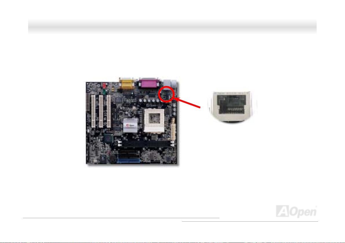
®
®
SSuuppppoorrtt IInntteel
This motherboard has a fast Ethernet controller on chip. On the strength of LAN chip onboard, it provides 10/100M bps Ethernet
for office and home use, the Ethernet connector is located on top of USB connectors.
l
PPRROO//110000 NNeettwwoorrkk CCoonnnneeccttiioonn ((OOppttiioonnaall))
OOnnlliinnee MMaannuuaall
46
Page 47
MMXX33WW--EE33 // MMXX33WW--VV33
OOnnlliinnee MMaannuuaall
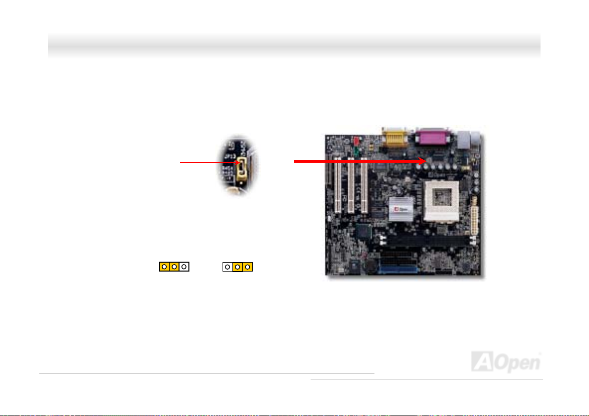
JJPP1133 LLAANN EEnnaabbllee // DDiissaabbllee SSeelleecctt JJuummppeerr ((OOppttiioonnaall))
This jumper allows you to enable or disable the LAN onboard function by adjusting the position of yellow cap.
Pin 1
1
Enable
(Default)
1
Disable
47
Page 48
MMXX33WW--EE33 // MMXX33WW--VV33
OOnnlliinnee MMaannuuaall
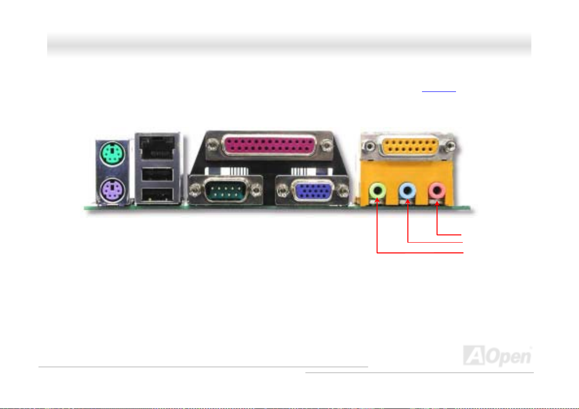
PPCC9999 CCoolloorr CCooddeedd BBaacckk PPaanneell
The onboard I/O devices are PS/2 Keyboard, PS/2 Mouse, serial ports COM1 and COM2, Printer, four USB, AC97 sound and
game port. The view angle of drawing shown here is from the back panel of the housing.
PS/2 Keyboard: For standard keyboard, which is using a PS/2 plug.
PS/2 Mo us e: Fo r PC- Mou s e, wh ic h is usi ng a P S/ 2 pl ug.
USB Por t : Available for connecting USB devices.
Parallel Port: To connect with SPP/ECP/EPP printer.
COM1 Port: To connect with pointing devices, modem or others serial devices.
VGA Connector: To connect with PC monitor.
Speaker Out: To External Speaker, Earphone or Amplifier.
Line-In: Comes from the signal sources, such as CD/Tape player.
MIC-In: From Microphone.
MIDI/Game Port: For 15-pin PC joystick, game pad or MIDI devices.
RJ-45 LAN Connector: To 10/100M bps Ethernet, Ethernet RJ45 connector
PS/2 Mouse
Connector
PS/2 Keyboard
Connector
RJ-45 LAN
Connector(Optional)
USB
Connectors
COM 1 Port
SPP/EPP/ECP
Parallel Port
Connector
MIDI/Game Port
VGA
MIC-In
Line-In
Speaker Out
48
Page 49

MMXX33WW--EE33 // MMXX33WW--VV33
OOnnlliinnee MMaannuuaall
DSR#
GND
CTS#
RTS#
RI#
CCOOMM22 CCoonnnneeccttoorr
This motherboard provides two serial ports. One of them are on back panel connector, the other is on the up-middle area of this
motherboard. With proper cable, you can connect it to the back panel of chassis.
Pin 1
DTR#
SIN
2
1
DCD#
SOUT
49
Page 50
MMXX33WW--EE33 // MMXX33WW--VV33
d
nnd
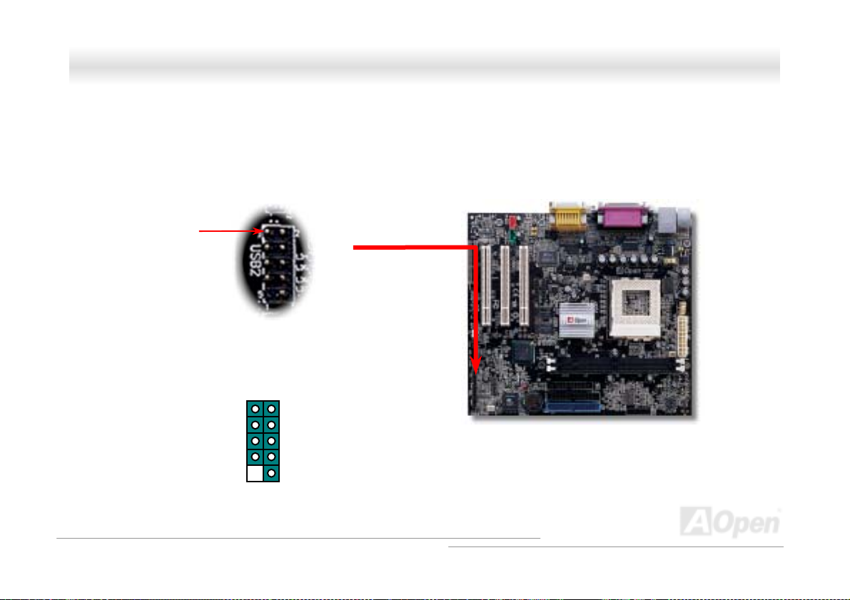
SSuuppppoorrtt 2
This motherboard supports four USB ports. Two of them are on back panel connector, the other two are on the left side of this
motherboard. With proper cable, you can connect them to front panel.
2
UUSSBB PPoorrtt
Pin 1
nd
2
USB Port Connector
+5V
SBD2-
SBD2+
GND
KEY
1 2
9 10
+5V
SBD3SBD3+
GND
NC
OOnnlliinnee MMaannuuaall
50
Page 51

MMXX33WW--EE33 // MMXX33WW--VV33
OOnnlliinnee MMaannuuaall
DDVVOO ((DDiiggiittaall VViiddeeoo OOuutt)) CCoonnnneeccttoorr
Through an external module attached to this DVO connector, you can connect a flat panel, digital CRT or 1.8V TV-Out interface.
Pin1
51
Page 52
1
MMXX33WW--EE33 // MMXX33WW--VV33
OOnnlliinnee MMaannuuaall
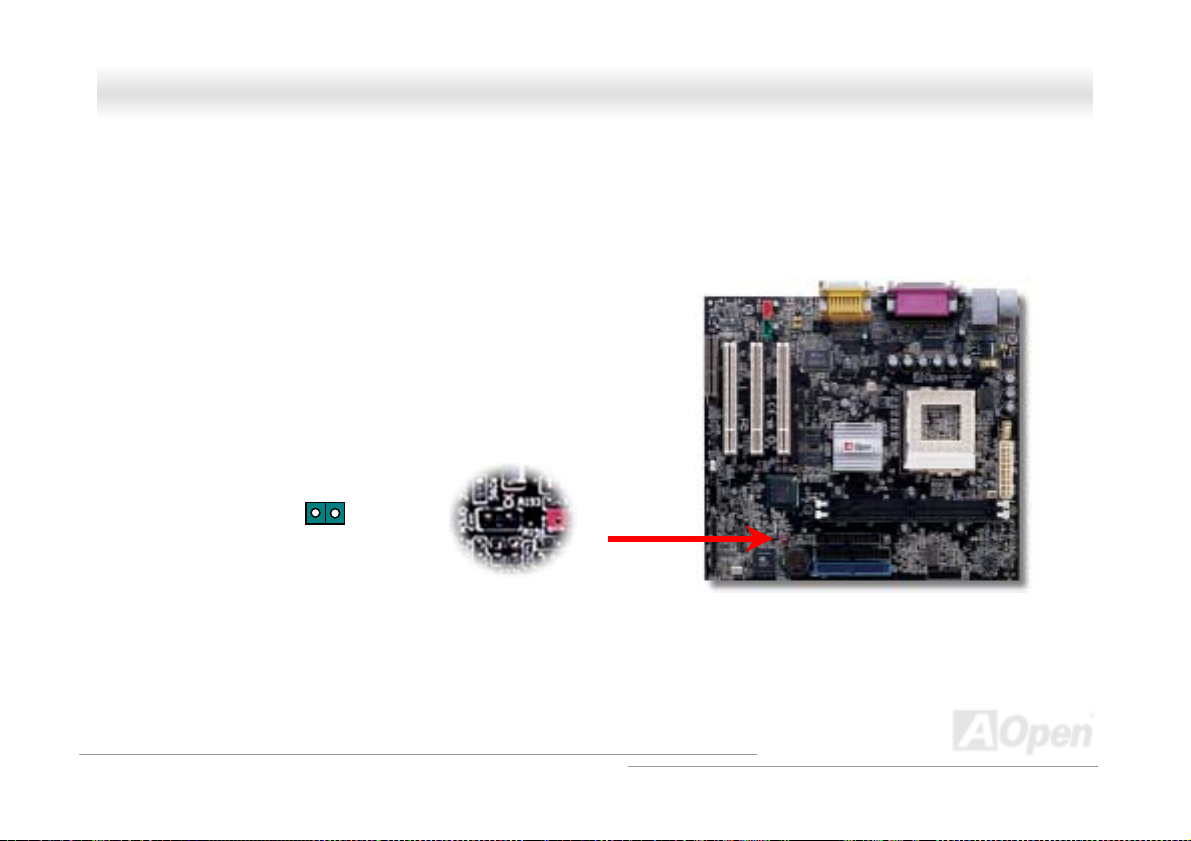
CChhaassssiiss IInnttrruussiioonn SSeennssoorr
The “CASE OPEN” header provides chassis intrusion-monitoring function. This function logged the event in the system BIOS
when chassis is opened. You can use the 2-pin chassis intrusion sensor to connect with this header, and enable the chassis
monitoring function of system BIOS.
SENSOR
Chassis I nt rus i on
Sensor Connector
GND
52
Page 53

MMXX33WW--EE33 // MMXX33WW--VV33
OOnnlliinnee MMaannuuaall
CCDD AAuuddiioo CCoonnnneeccttoorr
This connector is used to connect CD Audio cable from CDROM or DVD drive to onboard sound.
GND GND R
L
CD-IN
53
Page 54

MMXX33WW--EE33 // MMXX33WW--VV33
OOnnlliinnee MMaannuuaall
MMooddeemm AAuuddiioo CCoonnnneeccttoorr
This connector is used to connect Mono In/MIC Out cable from internal modem card to onboard sound circuit. The pin 1-2 is
Mono In, and the pin 3-4 is MIC Out. Please note that there is no standard for this kind of connector yet, only some internal
modem cards implement this connector.
MIC OUT
GND
GND
MONO IN
MODEM-CN
54
Page 55
MMXX33WW--EE33 // MMXX33WW--VV33
OOnnlliinnee MMaannuuaall
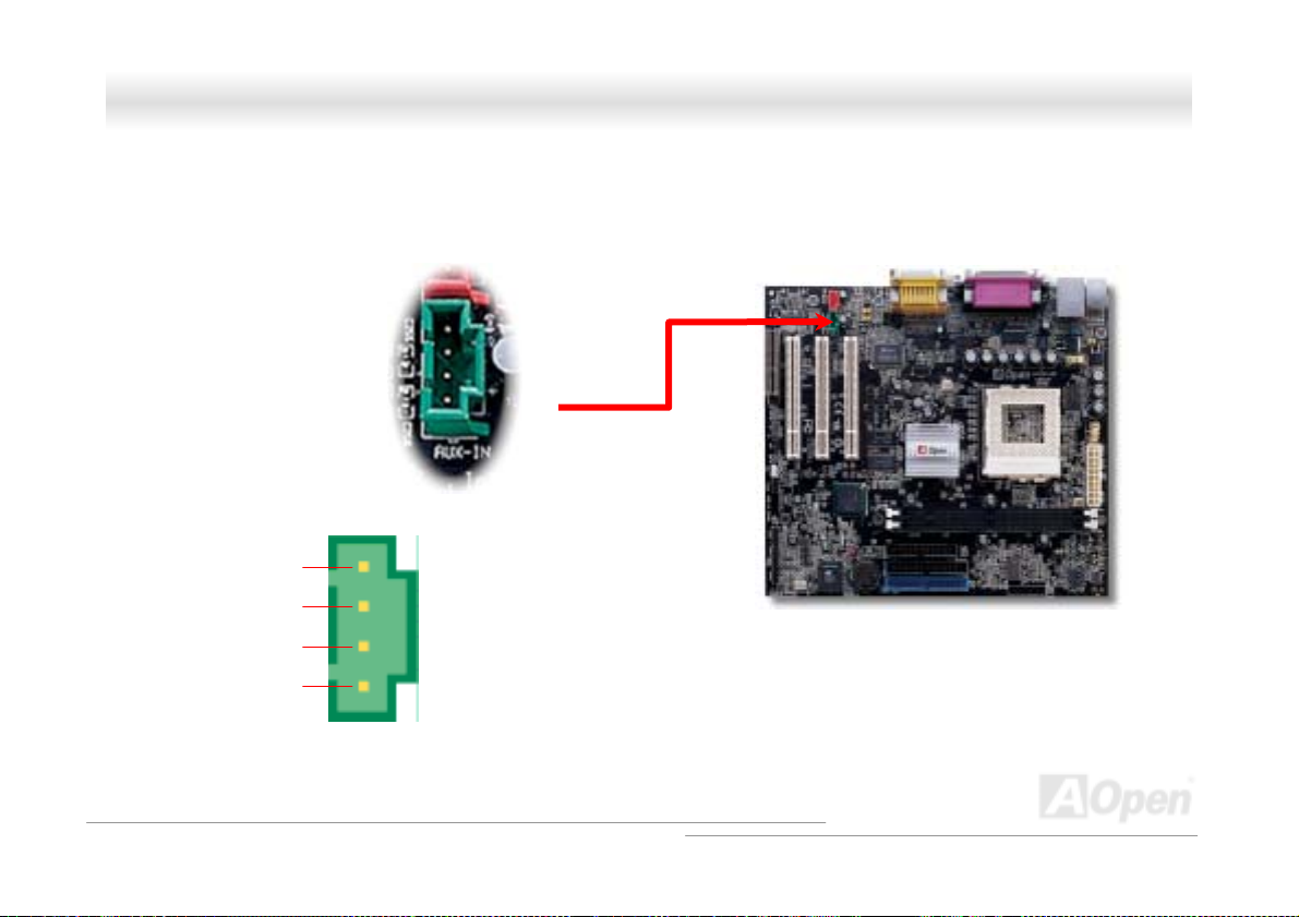
AAUUXX--IINN CCoonnnneeccttoorr
This connector is used to connect MPEG Audio cable from MPEG card to onboard sound.
R
GND
GND
L
AUX-IN
55
Page 56

p
MMXX33WW--EE33 // MMXX33WW--VV33
OOnnlliinnee MMaannuuaall
FFrroonntt AAuuddiioo CCoonnnneeccttoorr
If the housing has been designed with an audio port on the front panel, you’ll be able to connect onboard audio to front panel
through this connector.
MIC_IN2
MICBIAS2
FRONT_R
FRONT_L
NC
Pin 1
1 2
GND
+5V
RET_R
KEY
RET_L
9 10
Note: Please remove the jumper cap from the Front Audio
Connector before you connect the cable. Do not remove this
yellow jumper cap if housing without an audio port on the front
anel.
56
Page 57
MMXX33WW--EE33 // MMXX33WW--VV33
OOnnlliinnee MMaannuuaall
GGPPOO ((GGeenneerraall PPuurrppoossee OOuuttppuutt)) CCoonnnneeccttoorr
GPO (General Purpose Output) is an advanced specification developed by AOpen for power users to define the further
function by oneself. For example, you can design a daughter board to provide additional capabilities, such as an alarm, a buzzer,
a timekeeper, etc.
Pin 1
3.3V
GPO21
GPO19
1 2
NC
GND
5 6
57
Page 58
A
MMXX33WW--EE33 // MMXX33WW--VV33
OOnnlliinnee MMaannuuaall
Battery-less and Long Life Design
This Motherboard implements Flash ROM and a special circuit that allows you to save your current CPU and CMOS Setup
configurations without the need of a battery. The RTC (real time clock) can also keep running as long as the power cord is
plugged. If you lose your CMOS data by accident, you can just reload the CMOS configurations from Flash ROM and the system
will recover as usual.
Flash
ROM
ATX Stand-by Power Batter y
Auto Swi t ch
RTC
(Real Time Clock)
00:00:00
CMOS
Backup by EEPROM
uto switching to ATX standby
power as long as AC power line is
plugged. This smart design
increases battery life if you still plug
battery on motherboard.
58
Page 59
MMXX33WW--EE33 // MMXX33WW--VV33
OOnnlliinnee MMaannuuaall
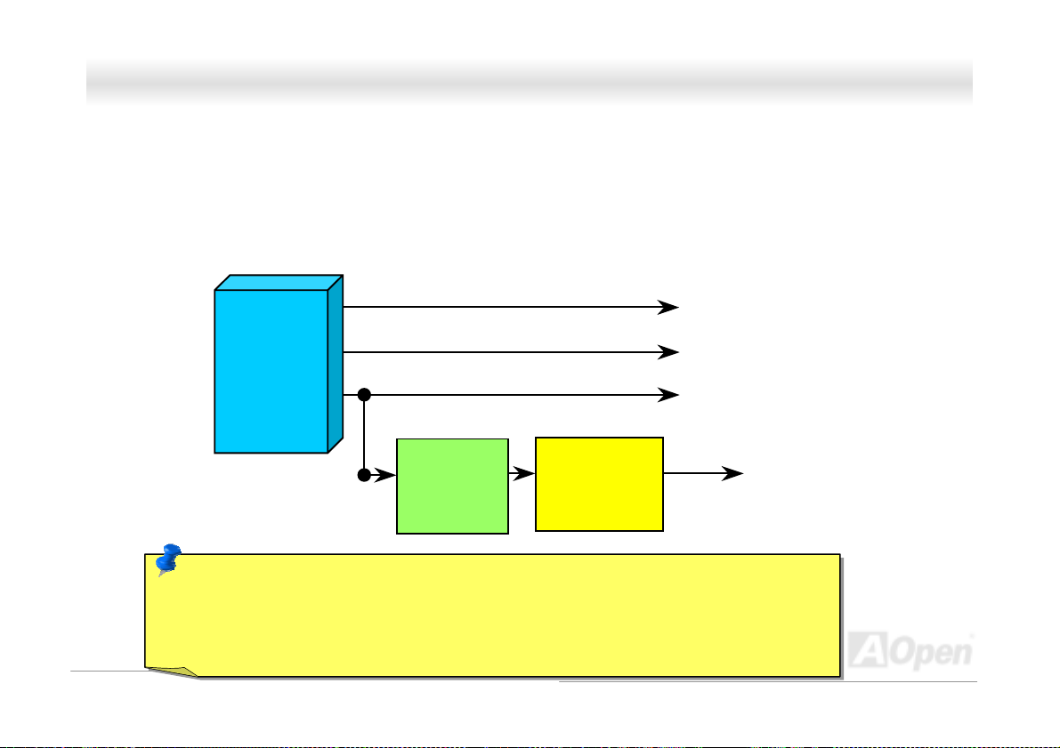
OOvveerr--ccuurrrreenntt PPrrootteeccttiioonn
The Over Current Protection was very popular implemented on ATX 3.3V/5V/12V switching power supply. However, the new
generation CPU uses different voltage that has regulator to transfer 5V to CPU voltage (for example, 2.0V), and makes 5V over
current protection useless. This motherboard is with switching regulator onboard supports CPU over-current protection; in
conjunction with 3.3V/5V/12V power supply provide the full line over-current protection.
Note: Although we have implemented protection circuit try to prevent any human operating
mistake, there is still certain risk that CPU, memory, HDD, add-on cards installed on this
motherboard may be damaged because of component failure, human operating error or unknown
nature reason. AOpen cannot guarantee the protection circuit will always work perfectly.
ATX
Switching
Power
Supply
12V (Protected by power supply)
3.3V (Protected by power supply)
5V (Protected by power supply)
Onboard
Power
Regulator
Over-Current
Protection
Circuit
CPU Core Voltage
59
Page 60
MMXX33WW--EE33 // MMXX33WW--VV33
OOnnlliinnee MMaannuuaall
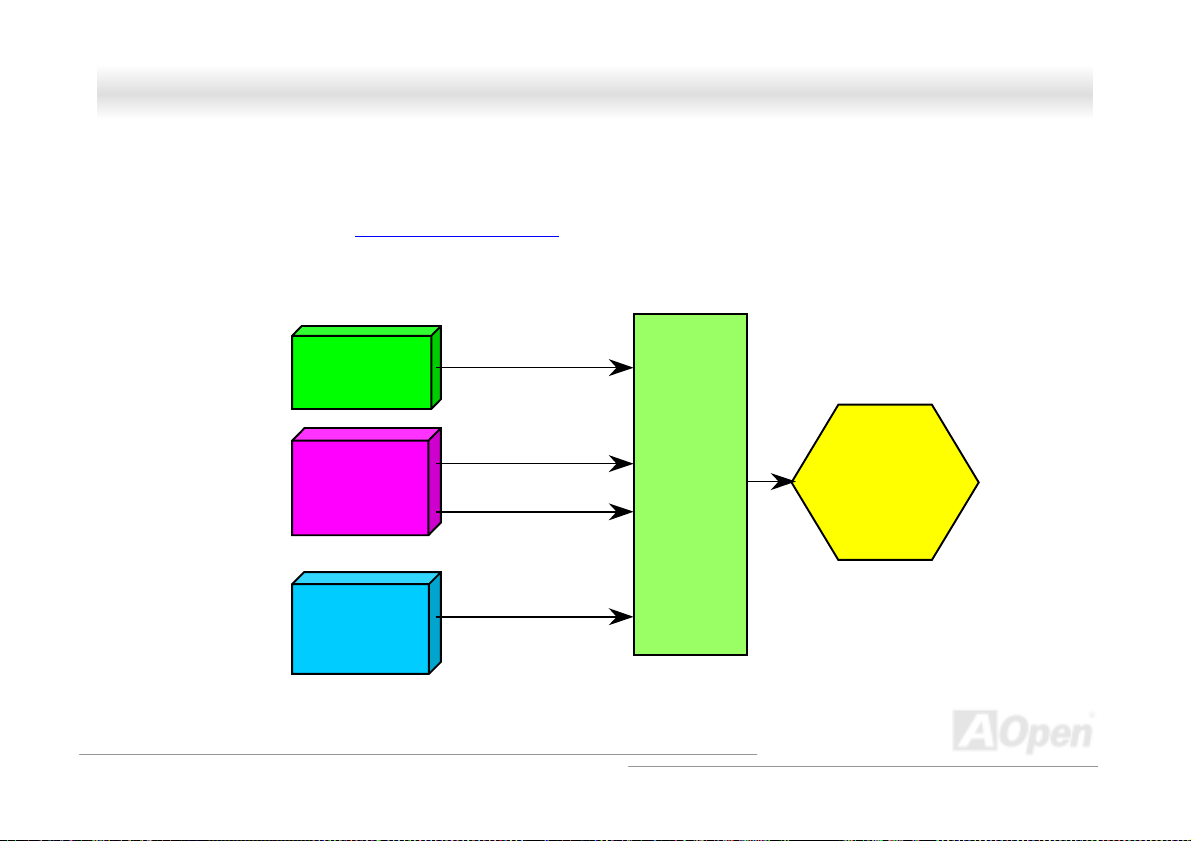
HHaarrddwwaarree MMoonniittoorriinngg
This motherboard implements a hardware monitoring system. As you turn on your system, this smart design will continue to
monitor your system’s working voltage, fan status and CPU temperature. If any of these systems’ status goes wrong, there will
be an alarm through the AOpen Hardware Monitoring Utility to warn the user.
Fan
CPU
Power
Fan Speed
AOpen H/W
Monitoring
Utility
CPU Temperature
CPU Voltage
System Voltage
Detection
Circuit
60
Page 61

MMXX33WW--EE33 // MMXX33WW--VV33
OOnnlliinnee MMaannuuaall
RReesseettttaabbllee FFuussee
Traditional motherboard has fuse for Keyboard and USB port to prevent over-current or shortage. These fuses are soldered
onboard that when it is broken (did the job to protect motherboard), user still cannot replace it and the motherboard is still
malfunction.
With expensive Resettable Fuse, the motherboard can back to normal function after fuse did the protection job.
Resettable
Fuse
61
Page 62
MMXX33WW--EE33 // MMXX33WW--VV33
OOnnlliinnee MMaannuuaall
LLooww EESSRR CCaappaacciittoorr
The quality of low ESR capacitor (Low Equivalent Series Resistance) during high frequency operation is very important for
stability of CPU power. The location of where to put these capacitors is another know-how that requires experience and detail
calculation.
62
Page 63
MMXX33WW--EE33 // MMXX33WW--VV33
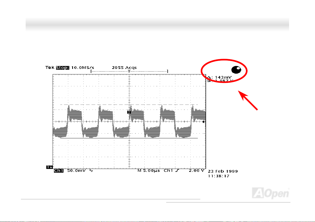
The power circuit of the CPU core voltage must be checked to ensure system stability for high speed CPUs (such as the new
Pentium III, or when overclocking). A typical CPU core voltage is 1.75V, so a good design should control voltage between 1.45V
and 1.8V. That is, the transient must be below 280mV. B elow is a timing diagram captured by a Digital Storage Scope, it shows
the voltage transient is only 143mv even when maximum 18A current is applied.
Note: This diagram is for example only; it may not be exactly the same as the motherboard you purchased.
OOnnlliinnee MMaannuuaall
63
Page 64
MMXX33WW--EE33 // MMXX33WW--VV33
OOnnlliinnee MMaannuuaall
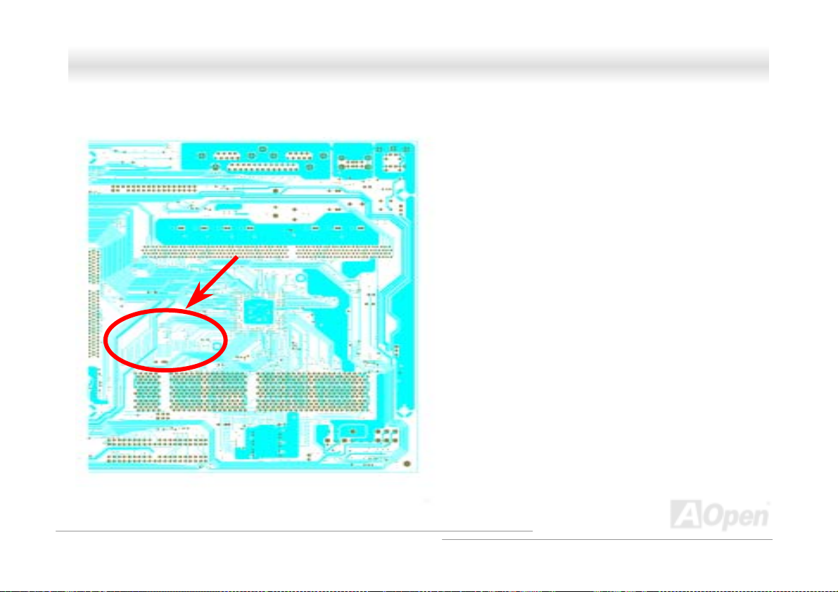
LLaayyoouutt ((FFrreeqquueennccyy IIssoollaattiioonn WWaallll))
Note: This diagram for example only, it may not be exactly
the same as this motherboard.
For high frequency operation, especially overclocking,
layout is the most important factor to make sure
chipset and CPU working in stable condition. The
layout of this motherboard implements AOpen’s
unique design called “ Frequency Isolation Wall”.
Separating each critical portion of motherboard into
regions where each region operates in a same or
similar frequency range to avoid cross talk and
frequency interference between each region’s
operations and condition. The trace length and route
must be calculated carefully. For example, the clock
trace must be equal length (not necessarily as short
64
as possible) so that clock skew will be controlled
within few a pico second (1/10
12
Sec)
Page 65

MMXX33WW--EE33 // MMXX33WW--VV33
OOnnlliinnee MMaannuuaall
DDrriivveerr aanndd UUttiilliittyy
There are motherboard drivers and utilities included in AOpen Bonus CD. You don’t need to install all of them in order to boot
your system. But after you finish the hardware installation, you have to install your operation system first (such as Windows 98)
before you can install any drivers or utilities. Please refer to your operation system’s installation guide.
Note: Please follow recommended procedure
to install Windows 95
and Windows 98.
65
Page 66
MMXX33WW--EE33 // MMXX33WW--VV33
OOnnlliinnee MMaannuuaall
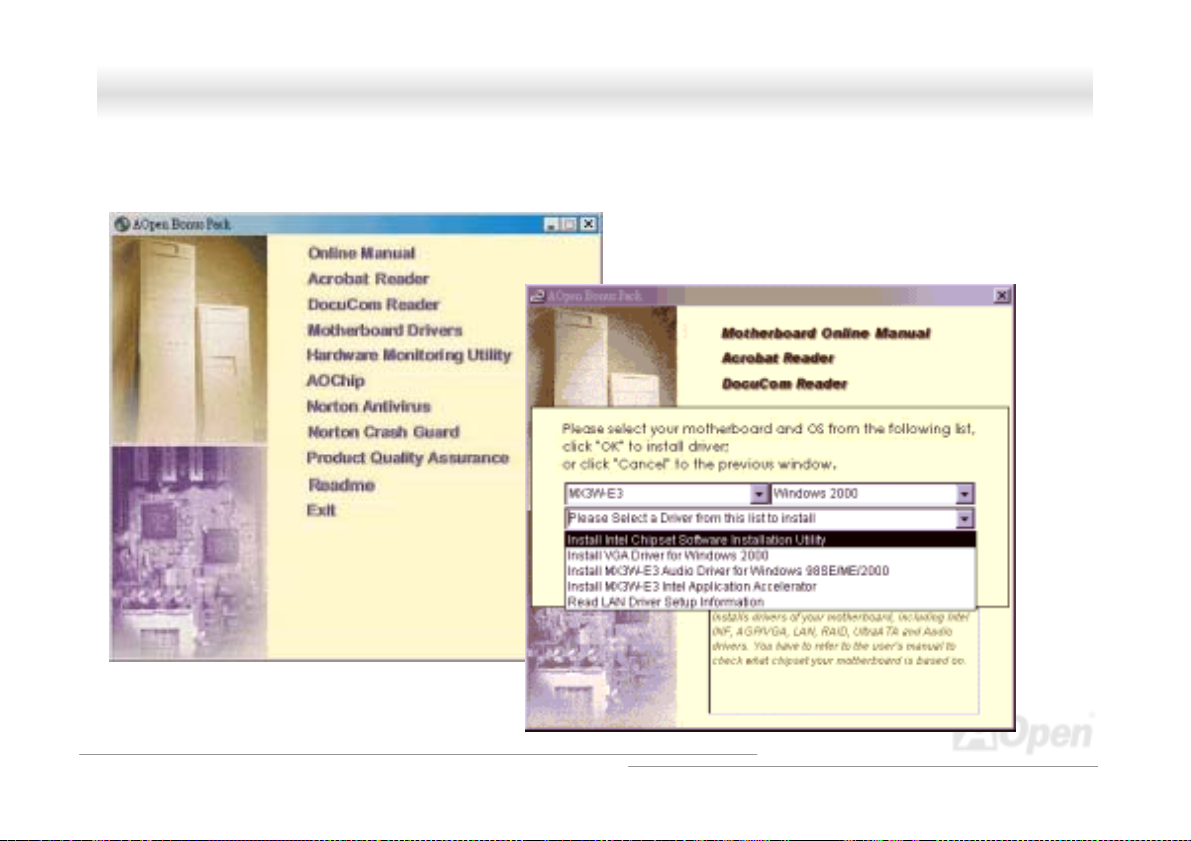
AAuuttoo--rruunn MMeennuu ffrroomm BBoonnuuss CCDD DDiisscc
You can use the auto-run menu of Bonus CD disc. Choose the utility and driver and select model name.
66
Page 67
MMXX33WW--EE33 // MMXX33WW--VV33
OOnnlliinnee MMaannuuaall
IInnssttaalllliinngg CChhiippsseett SSooffttwwaarree IInnssttaallllaattiioonn UUttiilliittyy
Windows 95/98 cannot recognize this chipset, because it was released prior to the Intel 810E and 810 chipsets. You can install
the Intel Chipset Software Installation Utility from the Bonus Pack CD disc auto-run menu to eliminate the “?” marks.
67
Page 68

MMXX33WW--EE33 // MMXX33WW--VV33
OOnnlliinnee MMaannuuaall
IInnssttaalllliinngg OOnnbbooaarrdd AAGGPP DDrriivveerr
Intel 810E and 810 chipsets integrate a 2D/3D graphics accelerator and provides AGP 1X/2X high performance to access
main memory at 533MB/s. You can find the audio driver from the Bonus Pack CD auto-run menu.
Note: If you are usin g Wind ows 95, y ou
should install DCOM95 patch from the
Bonus Pack auto-run menu first,
before you install AGP d
river.
68
Page 69

MMXX33WW--EE33 // MMXX33WW--VV33
OOnnlliinnee MMaannuuaall
IInnssttaalllliinngg IInntteell IIAAAA DDrriivveerr
You can install Intel IAA Driver to increase the performance of software applications and reduce PC boot times. You can find it
in the AOpen Bonus Pack CD
Note: Installing this ATA/100 IDE
driver may cause Suspend to
Hard Drive failure.
.
69
Page 70
MMXX33WW--EE33 // MMXX33WW--VV33
OOnnlliinnee MMaannuuaall
IInnssttaalllliinngg OOnnbbooaarrdd SSoouunndd DDrriivveerr
This motherboard comes with a Realtek ALC201 AC97 CODEC. You can find the audio driver from the Bonus Pack CD disc
auto-run menu.
70
Page 71

t
t
k
f
t
N
MMXX33WW--EE33 // MMXX33WW--VV33
OOnnlliinnee MMaannuuaall
IInnssttaalllliinngg LLAANN DDrriivveerr ((OOppttiioonnaall))
This motherboard integrates a total communication solution including 10/100Mb Fast Ethernet for Office requirement. You can
install LAN Driver under Windows95/98, Windows NT, Windows 2000 & Windows XP by following steps.
Manually Adding an Adapter in Windows 95 / 98 / ME / NT4 / 2000 / XP
=====================================
LOCATION OF DRIVER: \Driver\Lan\E100BNT5.SYS (NDIS 5.0)
LOCATION OF SETUP FILE: \Driver\Lan\NET82557.INF
1. From the Control Panel, double-click the “Add Hardware” icon.
2. Double-click Other Devices or Network Adapters in the list area.
3. Double-click a PCI Ethernet Controller.
4. Click the Driver tab, then click Update Driver.
5. Click Next at the Update Device Driver Wizard.
6. Select "Display a list of all the drivers..." and click Next.
7. Insert the AOpen Bonus CD and click Have Disk.
8. Enter the appropriate drive for your disk media
(for example: D:\) ,and click OK.
9. Click OK at the Select Device dialog box.
10. The Update Wizard displays the message that it has found
the driver. Click Next.
11. Click Finish and restart your computer when prompted.
Note: If the New Hardware
Found dialog box does no
appear at startup and you canno
connect to the network, chec
the Device Manager list to see i
the new adapter is present. If i
is not, please install the LA
driver manually.
71
Page 72
MMXX33WW--EE33 // MMXX33WW--VV33
OOnnlliinnee MMaannuuaall
IInnssttaalllliinngg HHaarrddwwaarree MMoonniittoorriinngg UUttiilliittyy
You can install Hardware Monitoring Utility to monitor CPU temperature, fans and system voltage. The hardware monitoring
function is automatically implemented by the BIOS and utility software. No hardware installation is needed.
72
Page 73

MMXX33WW--EE33 // MMXX33WW--VV33
OOnnlliinnee MMaannuuaall
AACCPPII SSuussppeenndd ttoo HHaarrdd DDrriivvee
ACPI Suspend to Hard Drive is basically controlled by Windows operation system. It sa ves your current work (system status,
memory and screen image) into hard disk, and then the system can be totally power off. Next time, when power is on, you can
resume your original work directly from hard disk within few seconds without go through the Windows booting process and run
your application again. If your memory is 64MB, normally, you need to reserve at least 64MB HDD space to save your memory
image.
When go into Suspend:
When power-on next time:
System
Image &
Status
System
Image &
Status
Hard
Disk
Save into
Restore within
seconds
Hard
Disk
73
Page 74

MMXX33WW--EE33 // MMXX33WW--VV33
OOnnlliinnee MMaannuuaall
System Requirement
1. AOZVHDD.EXE 1.30b or later.
2. Delete config.sys and autoexec.bat.
Fresh installation of Windows 98 on a new system
1. Execute "Setup.exe /p j" to install Windows 98
2. After Windows 98's installation is complete, go to the Control Panel > Power Management.
a. Set Power Schemes > System Standby to "Never".
b. Click on "Hibernate" and select "Enable Hibernate Support" then "Apply".
c. Click on the "Advanced" tab, you'll see "Hibernate" on "Power Buttons". Note that this option will only be seen after step
b mentioned above has been completed; otherwise only "Standby" and "Shutdown" will be shown. Select "Hibernate" and
"Apply".
3. Clean boot into DOS and run AOZVHDD utility.
a. If you ass ign the wh ole disk to your W in 98 system (FAT 16 or FAT 32), please r un "aozvhdd /c /file". Please remember
sufficient free space has to be reserved in the disk, e.g. if you have 64 MB DRAM and 16 MB VGA card installed, the
system needs at least 80 MB free space. The utility will locate the space automatically.
b. If you assign an individual partition for Win 98, please run "aozvhdd /c /partition". Of course, the system needs to
provid e unf orm at te d an emp ty pa rt iti o n.
4. Reboot sys tem .
5. You've already implemented ACPI Suspend to-Hard Drive. Click "Start > Shut Down > Standby" then the screen will go off
immediately. And 1 minute or so will be taken for the system to save what's in the memory to the hard drive; the larger the
memory size the longer this process will take.
74
Page 75

MMXX33WW--EE33 // MMXX33WW--VV33
OOnnlliinnee MMaannuuaall
Changing from APM to ACPI (Windows 98 only)
1. Run "Regedit.exe"
a. Go through the following path
HKEY_LOCAL_MACHINE
SOFTWARE
MICROSOFT
WINDOWS
CURRENT VERSION
DETECT
b. Select "ADD Binary" and name it as "ACPIOPTION".
c. Right click and select Modify, add "01" after "0000" to make it "0000 01".
d. Save changes.
2. Select "Add New Hardware" under Control Panel. Allow Windows 98 to detect new hardware. (It will find "ACPI BI O S " and
remove "Plug and Pla y BIOS")
3. Reboot sys tem .
4. Clean boot into DOS and run "AOZVHDD.EXE /C /File"
Changing from ACPI to APM
1. Run "Regedit.exe"
a. Go through the following path
75
Page 76

A
MMXX33WW--EE33 // MMXX33WW--VV33
HKEY_LOCAL_MACHINE
SOFTWARE
MICROSOFT
WINDOWS
CURRENT VERSION
b. Right click and select "Modify, change "01" to "02" to make it "0000 02".
c. Save changes.
2. Select "Add New Hardware" under Control Panel. Allow Windows 98 to detect new hardware. (It will find "Plug and Play
BIOS" and remove "ACPI BIOS")
3. Reboot sys tem .
4. Run "Add New Hardware" again and it will find "Advanced Power Management Resource".
5. Click "OK ".
Tip: "02" means Windows 98 is ACPI acknowledged
but the ACPI function is disabled.
Tip: Currently we found only ATI 3D Rage Pro AGP card would support
CPI suspend to disk. Please refer to AOpen web site for latest update
DETECT
ACPI OPTION
OOnnlliinnee MMaannuuaall
76
Page 77
MMXX33WW--EE33 // MMXX33WW--VV33
OOnnlliinnee MMaannuuaall
AACCPPII SSuussppeenndd ttoo RRAAMM ((SSTTRR))
This motherboard supports ACPI Suspend to RAM function. With this function, you can resume your original work directly from
DRAM without going through the Windows 98 booting process and run your application again. Suspend to DRAM saves your
current work in the system memory, it is faster than Suspend to Hard Drive but requires power supplied to DRAM, while
Suspend to Hard Drive requires no power.
When go into Suspend:
When power-on next time:
System Image & Status
in the DRAM
System Image & Status
in the DRAM
Backup by 3.3V
Power
Power back to
Other System
Devices
Other System
Devices
Power loss
Power back to
w
rk
77
Page 78

MMXX33WW--EE33 // MMXX33WW--VV33
To implement ACPI Suspend to DRAM, please follow the procedures as below:
OOnnlliinnee MMaannuuaall
System Requirement
1. An ACPI OS is required. Currently, except Windows95 and Windows NT all other Windows systems can support ACPI.
2. The Intel
®
Chipset Software Installation Utility must have been installed properly.
Procedures
1. Changed the following BIOS settings.
BIOS Setup > Power Management Setup > ACPI Function: Enabled
BIOS Setup > Power Management Setup > ACPI Suspend Type: S3.
2. Go to Control Panel > Power Management. Set “Power Buttons” to “Standby”.
3. Press power button or standby button to wake up the system.
78
Page 79
MMXX33WW--EE33 // MMXX33WW--VV33
OOnnlliinnee MMaannuuaall
AAWWAARRDD BBIIOOSS
System parameters can be modified by going into BIOS Setup m enu, this menu all ows yo u to conf igure t he syst em paramet ers
and save the configuration into the 128 bytes CMOS area, (normally in the RTC chip or in the mai n chipset).
The AwardBIOS™ that installed in the Flash RO M
BIOS provides critical low-level support for standard devices such as hard disk drives, serial and parallel ports.
Most BIOS setting of MX3WE3/MX3WV3 had optimized by AOpen’s R&D engineering team. But, the default setting of BIOS still can’t
fine-tune the chipset controlling entire system. Hence, the rest of this chapter is intended to guide you through the process of
config uri ng y ou r sys tem us in g set up.
To enter to BIOS setup menu, press <Del> when POST (Power-On Self Test) screen is shown on your monitor.
of the motherboard is a custom version of an industry standard BIOS. The
Note: Because the BIOS code is the most often
changed part of the motherboard design, the BIOS
information contained in this manual may be
different with actual BIOS that come with your
motherboard.
79
Page 80

g
MMXX33WW--EE33 // MMXX33WW--VV33
OOnnlliinnee MMaannuuaall
HHooww TToo UUssee AAwwaarrdd™™ BBIIOOSS SSeettuupp PPrrooggrraamm
Generally, you can use the arrow keys to highlight items that you want to choose, then press <Enter> key to select, and use the
<Page Up> and <Page Down> key to change setting value. You also can press <F1> key for help and press <Esc> key to quit
Award™ BIOS setup program. The following table provides details about how to use keyboard in the Award™ BIOS setup
program. By the way, all products of AOpen also provides a special function in the BIOS setup, you can press <F3> key
selecting preferred menu language to display.
Key Description
Page Up or + Changing setting to next value or increase the value.
Page Down or - Changing setting to previous value or decrease value.
Enter Select the item.
Esc 1. In main menu: Quit and don’t save any change.
2. In sub menu: Exit current menu to main menu.
Up Arrow Highlight previous item.
Down Arrow Highlight next item.
Left Arrow Move the light bar to left side of menu.
Right Arrow Move the light bar to right side of menu.
F1 Get menu or item help description.
F3 Changing menu language.
F5 Load previous setting value from CMOS.
F6 Load fail-save setting value from CMOS.
F7 Load turbo setting value from CMOS.
F10 Save changed setting and exit setup program.
Note: A Open always dedicates to give users a more
friendly computer system. Now, we include all
function descriptions of BIOS setup program into the
BIOS Flash ROM. When you select one function of
BIOS setup program, the function description will
appeared at right side of screen. Hence, you don’t
need read this manual while you changing the BIOS
settin
.
80
Page 81
MMXX33WW--EE33 // MMXX33WW--VV33
OOnnlliinnee MMaannuuaall
HHooww TToo EEnntteerr BBIIOOSS SSeettuupp
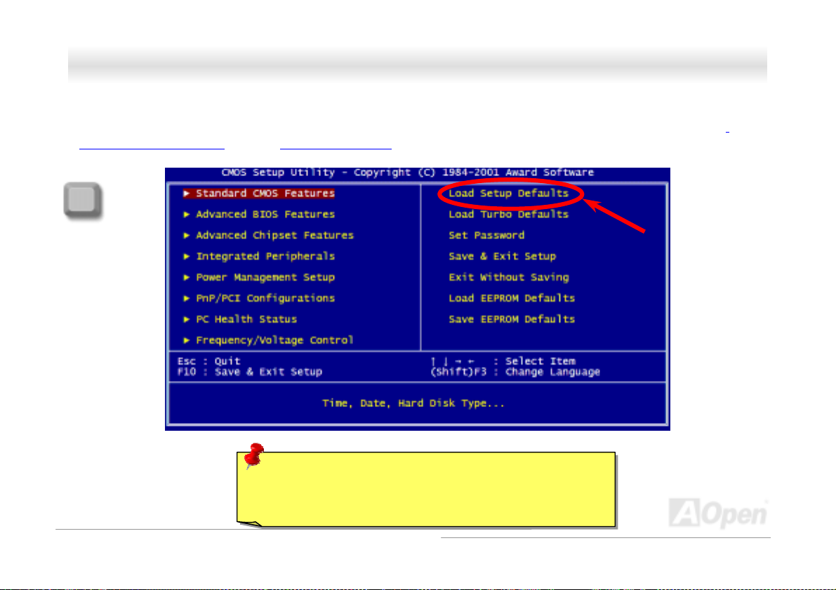
After you finish the setting of jumpers and connect correct cables. Power on and enter the BIOS Setup, press <Del> during
POST (Power-On Self Test). Choose "Load Setup Defaults" for recommended optimal performance.
Del
Warning: Please avoid of using "Load Turbo Defaults", unless
you are sure your system components (CPU, DRAM, HDD, etc.)
are good enough for turbo setting.
81
Page 82

MMXX33WW--EE33 // MMXX33WW--VV33
OOnnlliinnee MMaannuuaall
BBIIOOSS UUppggrraaddee
By flashing your motherboard, you agree to accept the possibility of BIOS flash failure. If you motherboard is working and is
stable, and there are no major bugs that were fixed by a latter BIOS revision, we recommend that you DO NOT try to upgrade
your BIOS.
By doing so, you are taking a risk of BIOS flash failure. If you indeed intent on upgrading, PLEASE BE SURE to use the right
BIOS revision for the right motherboard model.
AOpen Easy Flash is a little different than traditional flash method. The BIOS
and you simply run a single commend to complete the flash process.
binary file and flash routine are linked together
Caution: AOpen Easy Flash BIOS programs are designed to be
compatible with the Award BIOS. At the date of this note, AOpen
Easy Flash BIOS programs are not available for AMI BIOS. AMI
BIOS appears mostly only on old 486 boards and some early
Pentium boards. Please be sure to view the README compressed
inside the BIOS package before upgrading, and follow upgrade
instructions carefully. This will minimize the chance of flash
failures.
82
Page 83
MMXX33WW--EE33 // MMXX33WW--VV33
Below are the steps for easy flashing procedures: (applies for Award BIOS ONLY)
1. Download new BIOS upgrade zip
For example, MX3WE3102.ZIP.
2. Run shareware PKUNZIP (http://www.pkware.com/
binary BI OS f il e an d th e flas h uti li ty.
Or Winzip (http://www.winzip.com/
3. Save the unzipped file into a bootable floppy disk.
For example, MX3WE3102.BIN & MX3WE3102.EXE
4. Reboot the system to DOS mode without loading any memory handler (such as EMM386) or device driver. It needs
around 520K free memory spaces.
5. Execute A:> MX3WE3102 and the program will do the rest of it.
DO NOT turn off the power during FLASH PROCESS until you are asked to!!
6. Reboot system and press <Del> to enter BIOS setup
file from AOpen's web site.
) which supports miscellaneous operation systems to extract the
) in Windows environment.
, Choose "Load Setup Defaults", then “Save & Exit Setup”. Done!
Warning: The new BIOS upgrade will permanently replace your
original BIOS's settings and PnP information when flashing. You
may need to reconfigure your BIOS setting and re-install
Win95/Win98 as well as your add-on cards, so that your system
can go back to work as normal.
OOnnlliinnee MMaannuuaall
83
Page 84
MMXX33WW--EE33 // MMXX33WW--VV33
OOnnlliinnee MMaannuuaall
OOvveerrcclloocckkiinngg
As a leading manufacturer in motherboard industry, AOpen always listens to what customers want and develop products to fit
different user's requirements. Reliability, compatibility, leading technology and friendly features are our basic goals when
designing motherboards. Other than above mentioned design criteria, there are power users who are always seeking to push
the limitation of the system performance by overclocking which we call them "Overclocker".
This section is dedicated to overclockers.
This high performance motherboard is designed for maximum 133MHz CPU bus clock. But it comes with clock generator of
150MHz when we design it to accommodate future CPU bus clock. Our lab test results shown that 150MHz is achievabl e when
proper setting and qualified components were presented, we feel quite comfortable overclocking to 150MHz. Not only that, this
motherboard has full-range (CPU core voltage) settings and an option to adjust CPU core voltage. The CPU clock ratio can be
up to 8x that supports almost all of Pentium III/Celeron CPUs in the future and provides flexibility for overclockers. For your
reference, the following configurations are what we feel comfortable at 150MHz bus clock.
But no guaranty. ☺
Tip: Note that overclocking may also
cause thermal problem. Please make
sure that the cooling fan and the
heatsink were adequate to dissipate
excessive heat that's generated by
overclocking the CPU.
Warning: The design of this product follows CPU and chipset vendor's
design guideline. Any attempts to push beyond product specification are
not recommended and you are taking your own risk to damage your
system or important data. Before doing overclocking, you must make sure
your components are able to tolerate such abnormal setting, especially
CPU, DRAMs, hard disks, and AGP VGA cards.
84
Page 85

MMXX33WW--EE33 // MMXX33WW--VV33
OOnnlliinnee MMaannuuaall
VVGGAA CCaarrdd && HHaarrdd DDiisskk
VGA and HDD is key components for overclocking, for your reference, the following list are what have been successful
overclocked in our lab. Please note that AOpen can not guaranty they can be successful overclocked again. Please check the
Available Vendor List ( AVL) by link to our official website.
VGA: http://www.aopen.com.tw/tech/report/overclk/mb/vga-oc.htm
HDD: http://www.aopen.com.tw/tech/report/overclk/mb/hdd-oc.htm
85
Page 86

MMXX33WW--EE33 // MMXX33WW--VV33
OOnnlliinnee MMaannuuaall
GGlloossssaarryy
AACC9977
Basically, AC97 specification separates sound/modem circuit to two parts, digital processor and a CODEC for analogy I/O they
are linked by AC97 link bus. Since digital processor can be put into motherboard main chipset, the cost of sound/modem
onboard solution can be reduced.
AACCPPII ((AAddvvaanncceedd CCoonnffiigguurraattiioonn && PPoowweerr IInntteerrffaaccee))
ACPI is the power management specification of PC97 (1997). It intends to save m ore power by taking full control of power
management to operating system and bypass BIOS
to operating system (such as Windows 98). This is a bit similar as the PnP
power switch to control the power state transition.
AAGGPP ((AAcccceelleerraatteedd GGrraapphhiicc PPoorrtt))
AGP is a bus interface targeted for high-performance 3D graphic. AGP supports only memory read/write operation and
single-master single-slave one-to-one only. AGP uses both rising and falling edge of the 66MHz clock, for 2X AGP, the data
transfer rate is 66MHz x 4byte x 2 = 528MB/s. AGP is now moving to 4X mode, 66MHz x 4byte x 4 = 1056MB/s. AOpen is the
first company to support 4X A GP motherboards by both AX6C (Intel 820) and MX64/AX64 (VIA 694x), started from Oct 1999.
. The chipset or super I/O chip needs to provide standard register interface
register interface. ACPI defines ATX momentary soft
86
Page 87

MMXX33WW--EE33 // MMXX33WW--VV33
OOnnlliinnee MMaannuuaall
AAMMRR ((AAuuddiioo//MMooddeemm RRiisseerr))
The CODEC circuit of AC97 sound/modem solution can be put on motherboard or put on a riser card (AMR card) that connects
to motherboard through AMR connector.
AAOOppeenn BBoonnuuss PPaacckk CCDD
A disc bundled with AOpen motherboard product, there are motherboard drivers, Acrobat Reader for PDF online manual and
other us ef ul ut il iti es .
AAPPMM ((AAddvvaanncceedd PPoowweerr MMaannaaggeemmeenntt))
Unlike ACPI, BIOS controls most APM power management functions. AOpen Suspend to Hard Drive is a good example of APM
power management.
AATTAA ((AATT AAttttaacchhmmeenntt))
ATA is the specification of diskette interface. In 80’s, many software and hardware manufacturers instituted the ATA specificat ion
together. The AT is meaning International Business Machines Corporation (IBM) personal computer/AT’s bus structure.
AATTAA//6666
ATA/66 uses both rising edge and falling edge but doubles UDMA/33 transfer rate. The data transfer rate is 4 times of the PIO
mode 4 or DMA mode 2, 16.6MB/s x4 = 66MB/s. To use ATA/66, you need special ATA/66 IDE cable.
87
Page 88

MMXX33WW--EE33 // MMXX33WW--VV33
OOnnlliinnee MMaannuuaall
AATTAA//110000
ATA/100 is a new IDE specification under developing. ATA/100 uses both rising edge and falling edge as ATA/66 but clock cycle
time is reduced to 40ns. The data transfer rate is (1/40ns) x 2 bytes x 2 = 100MB/s. To use ATA/100, you need special 80-wire
IDE cab l e, t h e s ame as ATA/66.
BBIIOOSS ((BBaassiicc IInnppuutt//OOuuttppuutt SSyysstteemm))
BIOS is a set of assembly routine/program that reside in EPROM or Flash ROM. BIOS controls Input/output devices and other
hardware devices of motherboard. In general, to provide hardware independent portability, operation system and drivers is
required to access BIOS without directly access hardware devices.
BBuuss MMaasstteerr IIDDEE ((DDMMAA mmooddee))
The traditional PIO (Programmable I/O) IDE requires the CPU to involve in all the activities of the IDE access including waiting
for the mechanical events. To reduce the workload of the CPU, the bus master IDE device transfers data from/to memory
without interrupting CPU, and releases CPU to operate concurrently while data is transferring between memory and IDE device.
You need the bus master IDE driver and the bus master IDE HDD to support bus master IDE mode.
CCNNRR ((CCoommmmuunniiccaattiioonn aanndd NNeettwwoorrkkiinngg RRiisseerr))
The CNR specification provides the PC industry the opportunity to deliver a flexible and cost reduced method of implementing
LAN, home networking, DSL, USB, wireless, audio and modem subsystems widely used in today's "connected PCs". The CNR
specification is an open industry specification and is supported by OEMs, IHV card manufacturers, silicon supplier and
Microsoft.
88
Page 89

MMXX33WW--EE33 // MMXX33WW--VV33
OOnnlliinnee MMaannuuaall
CCOODDEECC ((CCooddiinngg aanndd DDeeccooddiinngg))
Normally, CODEC means a circuit that can do digital to analog conversion and also the analog to digital conversion. It is part of
sound/modem solution.
AC97
DDDDRR ((DDoouubbllee DDaattaa RRaatteedd)) SSDDRRAAMM
DDR SDRAM utilizes the existing DRAM infrastructure and technology while doubling the nominal bandwidth available to
systems in an easy to design and simple to adopt way. Initially a perfect solution for memory intensive server and workstation
applications, DDR low cost and low voltage will ultimately make it an ideal solution for all segments of the PC market, high
performance desktop and mobile PCs, Val ue PCs and even Internet Appliances and mobile devices.
DDIIMMMM ((DDuuaall IInn LLiinnee MMeemmoorryy MMoodduullee))
DIMM socket has total 168-pin and supports 64-bit data. It can be single or double side, the golden finger signals on each side
of PCB are different, and that is why it was called Dual In Line. Almost all DIMMs are made by SDRAM
Note that some old DIMMs are made by FPM/EDO
DDMMAA ((DDiirreecctt MMeemmoorryy AAcccceessss))
Channel for communications between the memory and surrounding devices.
, which operate at 3.3V.
and only operate at 5V. Do not confuse them with SDRAM DIMM.
89
Page 90

MMXX33WW--EE33 // MMXX33WW--VV33
OOnnlliinnee MMaannuuaall
EECCCC ((EErrrroorr CChheecckkiinngg aanndd CCoorrrreeccttiioonn))
The ECC mode needs 8 ECC bits for 64-bit data. Each time memory is accessed; ECC bits are updated and checked by a
special algorithm. The ECC algorithm has the ability to detect double-bit error and automatically correct single-bit error while
parity mode can only detect single-bit error.
EEDDOO ((EExxtteennddeedd DDaattaa OOuuttppuutt)) MMeemmoorryy
The EDO DRAM technology is actually very similar to FPM (Fast Page Mode). Unlike traditional FPM that tri-states the memory
output data to start the pre-charge activity, EDO DRAM holds the memory data valid until the next memory access cycle, that is
similar to pipeline effect and reduces one clock state.
EEEEPPRROOMM ((EElleeccttrroonniicc EErraassaabbllee PPrrooggrraammmmaabbllee RROOMM))
Also known as E2PROM. Both EEPROM and Flash ROM can be re-programmed by electronic signals, but the interface
technology is different. Size of EEPROM is much smaller than flash ROM.
EEPPRROOMM ((EErraassaabbllee PPrrooggrraammmmaabbllee RROOMM))
Traditional motherboard stores BIOS code in EPROM. EPROM can only be erased by ultra-violet (UV) light. If BIOS has to be
upgraded, you need to remove EPROM from motherboard, clear by UV light, re-program, and then insert back.
90
Page 91

MMXX33WW--EE33 // MMXX33WW--VV33
OOnnlliinnee MMaannuuaall
EEVV66 BBuuss
EV6 Bus in the technology of Alpha processor from Digital Equipment Corporation. EV6 bus uses both rising and falling clock
edge to transfer data, similar as DDR SDRAM or ATA/66 IDE bus.
EV6 Bus Speed = CPU external bus clock x 2.
For example, 200 MHz EV6 bus is actually using 100 MHz external bus clock, but the equivalent speed is 200 MHz.
FFCCCC DDooCC ((DDeeccllaarraattiioonn ooff CCoonnffoorrmmiittyy))
The DoC is component certification standard of FCC EMI regulations. This standard allows DIY component (such as
motherboard) to apply DoC label separately without a shielding of housing.
FFCC--PPGGAA ((FFlliipp CChhiipp--PPiinn GGrriidd AArrrraayy))
FC means Flip Chip, FC-PGA is a new package of Intel for Pentium III CPU. It can plug into SKT370 socket, but require
motherboard to add some signals on socket 370. That is, the motherboard needs to be redesigned. Intel is going to ship
FC-PGA 370 CPU and phase out slot1 CPU.
FFllaasshh RROOMM
Flash ROM can be re-programmed by electronic signals. It is easier for BIOS to upgrade by a flash utility, but it is also easier to
be infected by virus. Because of increase of new functions, BIOS size is increased from 64KB to 256KB (2M bit). AOpen AX5T is
the first board to implement 256KB (2Mbit) Flash ROM. Now flash ROM size is moving to 4M bit on AX6C (Intel 820) and MX3W
(Intel 810) motherboard. , AOpen motherboard uses EEPROM for jumper-less and battery-less design.
91
Page 92

MMXX33WW--EE33 // MMXX33WW--VV33
OOnnlliinnee MMaannuuaall
FFSSBB ((FFrroonntt SSiiddee BBuuss)) CClloocckk
FSB Clock means CPU external bus clock.
CPU internal clock = CPU FSB Clock x CPU Clock Ratio
2
2
I
I
CC BBuuss
See SMBus.
IIEEEEEE 11339944
IEEE 1394 is a low-cost digital interface originated by Apple Computer as a desktop LAN and developed by the IEEE 1394
working group. The IEEE 1394 can transport data at 100, 200 or 400 Mbps. One of the solutions to connect digital television
devices together at 200 Mbps. Serial Bus Management provides overall configuration control of the serial bus in the form of
optimizing arbitration timing, guarantee of adequate electrical power for all devices on the bus, assignment of isochronous
channel ID, and notification of errors. There are two type of IEEE 1394 data transfer: asynchronous and isochronous.
Asynchronous transport is the traditional computer memory-mapped, load and store interface. Data requests are sent to a
specific address and an acknowledgment is returned. In addition to an architecture that scales with silicon technology, IEEE
1394 features a unique isochronous data channel interface. Isochronous data channels provide guaranteed data transport at a
pre-determined rate. This is especially important for time-critical multimedia data where just-in-time delivery eliminates the need
for costly buffering.
92
Page 93

MMXX33WW--EE33 // MMXX33WW--VV33
OOnnlliinnee MMaannuuaall
PPaarriittyy BBiitt
The parity mode uses 1 parity bit for each byte, normally it is even parity mode, that is, each time the memory data is updated,
parity bi t will be adjust ed to have e ven count "1" for ea ch byte . When next time, if memory i s read wit h odd num ber of "1", the
parity error is occurred and this is called single bit error detection.
PPBBSSRRAAMM ((PPiippeelliinneedd BBuurrsstt SSRRAAMM))
For Socket 7 CPU, one burst data read requires four QWord (Quad-word, 4x16 = 64 bits). PBSRAM only needs one address
decoding time and automatically sends the remaining QWords to CPU according to a predefined sequence. Normally, it is
3-1-1-1, total 6 clocks, which is faster than asynchronous SRAM. PBSRAM is often used on L2 (level 2) cache of Socket 7 CPU.
Slot 1 and Socket 370 CPU do not need PBSRAM.
PPCC--110000 DDIIMMMM
SDRAM DIMM that supports 100MHz CPU FSB bus clock.
PPCC--113333 DDIIMMMM
SDRAM DIMM that supports 133MHz CPU FSB bus clock.
PPCC--11660000 oorr PPCC--22110000 DDDDRR DDRRAAMM
Based on FSB frequency, the DDR DRAM has 200MHz and 266MHz two type of working frequency. Because of DDR DRAM
data bus is 64-bit, it provides data transfer bandwidth up to 200x64/8=1600MB/s, and 266x64/8=2100MB/s. Hence, the PC-1600
DDR DRAM is working with 100MHz and PC-2100 DDR DRAM is working with 133MHz FSB frequency.
93
Page 94

MMXX33WW--EE33 // MMXX33WW--VV33
PPCCII ((PPeerriipphheerraall CCoommppoonneenntt IInntteerrffaaccee)) BBuuss
Bus for the internal connection of peripheral devices, high-speed data channel between the computer and expansion card.
PPDDFF FFoorrmmaatt
A file format for electronic document, PDF format is independent from platform, you can read PDF file under Windows, Unix,
Linux, Mac … with different PDF reader. You can also read PDF file by web browser such as IE and Netscape, note that you
need to install PDF plug-in first (Included in Acrobat Reader).
PPnnPP ((PPlluugg aanndd PPllaayy))
The PnP specification suggests a standard register interface for both BIOS and operating system (such as W indows 95). These
registers are used by BIOS and operating system to configure system resource and prevent any conflicts. PnP BIOS or
operating system will automatically allocate the IRQ/DMA/Memory. Currently, almost all the PCI cards and most ISA cards are
already PnP compliant.
PPOOSSTT ((PPoowweerr--OOnn SSeellff TTeesstt))
The BIOS self-test procedure after power-on, sometimes, it is the first or the second screen shown on your monitor during
system boot.
OOnnlliinnee MMaannuuaall
94
Page 95

MMXX33WW--EE33 // MMXX33WW--VV33
OOnnlliinnee MMaannuuaall
RRDDRRAAMM ((RRaammbbuuss DDRRAAMM))
Rambus is a memory technology that uses large burst mode data transfer. Theoretically, the data transfer should be high than
. RDRAM is cascaded in channel operation. For Intel 820, only one RDRAM channel is supported, 16-bit data per
SDRAM
channel, and this channel may have maximum 32 RDRAM devices, no matter how many RIMM
RRIIMMMM ((RRaammbbuuss IInnlliinnee MMeemmoorryy MMoodduullee))
184-pin memory module that supports RDRAM memory technology. A RIMM memory module may contain up to maximum of 16
RDRAM devices.
SSDDRRAAMM ((SSyynncchhrroonnoouuss DDRRAAMM))
SDRAM is one of the DRAM technologies that allow DRAM to use the same clock as the CPU host bus (EDO and FPM are
asynchronous and do not have clock signal). It is similar as PBSRAM
168-pin DIMM
SShhaaddooww E
A memory space in Flash-ROM to simulate E2PROM operation, AOpen motherboard uses Shadow E2PROM fo r jum per -less and
battery-less design
and operates at 3.3V. AOpen is the first company to support dual-SDRAM DIMMs onboard (AP5V), from Q1 1996
2
2
E
PPRROOMM
sockets.
to use burst mode transfer. SDRAM comes in 64-bit
95
Page 96

MMXX33WW--EE33 // MMXX33WW--VV33
OOnnlliinnee MMaannuuaall
SSIIMMMM ((SSiinnggllee IInn LLiinnee MMeemmoorryy MMoodduullee))
SIMM socket is only 72-pin, and is only single side. The golden finger signals on each side of PCB are identical. That is why it
was called Single In Line. SIMM is made by FPM or EDO
current motherboard design.
SSMMBBuuss ((SSyysstteemm MMaannaaggeemmeenntt BBuuss))
SMBus is also called I2C bus. It is a two-wire bus developed for component communication (especially for semiconductor IC).
For example, set clock of clock generator for jumper-less motherboard. The data transfer rate of SMBus is only 100Kbit/s, it
allows one host to communicate with CPU and many masters and slaves to send/receive message.
SSPPDD ((SSeerriiaall PPrreesseennccee DDeetteecctt))
SPD is a small ROM or EEPROM device resided on the DIMM or RIMM. S PD st ores mem ory module i nformation such as DRAM
timing and chip parameters. SPD can be used by BIOS
DRAM and supports 32-bit data. SIMM had been phased out on
to decide best timing for this DIMM or RIMM.
96
Page 97

MMXX33WW--EE33 // MMXX33WW--VV33
OOnnlliinnee MMaannuuaall
UUllttrraa DDMMAA
Ultra DMA (or, more accurately, Ultra DMA/33) is a protocol for transferring data between a hard disk drive through the
computer’s data path (or bus) to the computer’s random access memory (RAM). The Ultra DMA/33 protocol transfers data in
burst mode at a rate of 33.3MB/s, twice as fast as the previous Direct Memory Access (DMA)
developed as a proposed industry standard by the Quantum corporation, makes of hard disk drives, and Intel, makes of chipset
that support computer bus technology. Ultra DMA support in your computer means that it will boot (start) and open new
applications more quickly. It will help users of graphic-intensive and applications that require large amounts of access to data on
the hard disk drive. Ultra DMA uses Cyclical Redundancy Checking (CRC), offering a new level of data protection. Ultra DMA
uses the s am e 40 -pi n ID E int e rfac e c abl e as P IO a nd D MA.
16.6MB/s x2 = 33MB/s
16.6MB/s x4 = 66MB/s
16.6MB/s x6 = 100MB/s
UUSSBB ((UUnniivveerrssaall SSeerriiaall BBuuss))
USB is a 4-pin serial peripheral bus that is capable of cascading low/medium speed peripherals (less than 10Mbit/s) such as
keyboard, mouse, joystick, scanner, printer and modem. With USB, the traditional complex cables from back panel of your PC
can be elim i nat ed .
interface. Ultra DMA was
97
Page 98

MMXX33WW--EE33 // MMXX33WW--VV33
OOnnlliinnee MMaannuuaall
VVCCMM ((VViirrttuuaall CChhaannnneell MMeemmoorryy))
NEC’s Virtual Channel Memory (VCM) is a new DRAM core architecture that dramatically improves the memory system’s ability
to service multimedia requirements. VCM increases memory bus efficiency and performance of any DRAM technology by
providing a set of fast static registers between the memory core and I/O pins. Using VCM technology results in reduced data
access latency and reduced power consumption.
ZZIIPP ffiillee
A compressed file format that can reduce the file size. To unzip file, run shareware PKUNZIP (http://www.pkware.com/) for DOS
and other operating system or WINZIP (http://www.winzip.com/
) for windows environment.
98
Page 99

MMXX33WW--EE33 // MMXX33WW--VV33
OOnnlliinnee MMaannuuaall
TTrroouubblleesshhoooottiinngg
If you encounter any trouble to boot you system, follow the procedures accordingly to resolve the problem.
Turn off the power and unplug the AC power cable, then remove all of the add-on
cards and cables, including VGA, IDE, FDD, COM1, COM2 and printer.
Make sure if all jumper settings are correct.
Clear CMOS
Start
Next
99
Page 100
MMXX33WW--EE33 // MMXX33WW--VV33
Yes No
Install the VGA card. Then connect your monitor and keyboard.
Next
Continue
Turn on the power
and check if the power
supply and CPU fan work
properly.
The problem is probably caused by
power supply or motherboard failure
Please contact your reseller or local
distributor for repairing.
OOnnlliinnee MMaannuuaall
.
100
 Loading...