

Page 1
MMXX334
4
OOn
n
iinne
e
MMaan
n
a
a
MX34
DOC. NO. : MX34-OL-E0103D
l
l
u
u
ll
1
Page 2

MMXX334
4
OOn
n
iinne
e
MMaan
n
a
a
l
l
u
u
ll
WWhhaatt’’ss iinn tthhiiss mmaannuuaall
MX34......................................................................................................1
What’s in this manua l..........................................................................................................................2
Before You Start..................................................................................................................................8
Quick Installat ion Proc ed ure ..............................................................................................................9
Motherboard Map ................................................................................................................ .............10
Block Diagram...................................................................................................................................11
Hardware.............................................................................................12
JP14 Clear CMOS............................................................................................................................13
CPU Socket ......................................................................................................................................14
CPU Fan and Housing Fan Connector ............................................................................................15
CPU Jumper-less Design .................................................................................................................16
JP29/JP23 FSB/PCI Clock Ratio .....................................................................................................19
DIMM Socket ....................................................................................................................................21
Front Panel Connector .....................................................................................................................23
ATX Power Connector ......................................................................................................................25
2
Page 3

MMXX334
4
OOn
n
iinne
e
MMaan
n
a
a
AC Power Auto Recovery.................................................................................................................26
IDE and Floppy Connector ...............................................................................................................27
IrDA Connector .................................................................................................................................30
WOM (Zero Voltage Wake on Modem)............................................................................................31
WOL (Wake on LAN)........................................................................................................................34
4X AGP (Accelerated Graphic Port).................................................................................................36
PC99 Color Coded Back Panel........................................................................................................37
Support 4 USB Ports ........................................................................................................................38
JP12 Enable/Disable Onboard Sound .............................................................................................39
CD Audio Connector.........................................................................................................................40
AUX-IN Connector............................................................................................................................41
Modem Audio Connector..................................................................................................................42
Front Audio Connector......................................................................................................................43
Battery-les s and Long Life Design...................................................................................................44
Over-current Protection ....................................................................................................................45
Hardware Monitoring ........................................................................................................................47
l
l
u
u
ll
3
Page 4

MMXX334
4
OOn
n
iinne
e
MMaan
n
a
a
Driver and Utility..................................................................................54
AWAR D BIOS........................................................................................71
Resettable Fuse................................................................................................................................48
Year 2000 (Y2K) ...............................................................................................................................49
1500uF Low ESR Capacitor.............................................................................................................51
Layout (Frequency Isolation Wall)....................................................................................................53
Autorun Menu from Bonus CD Disc.................................................................................................55
Installing Windows 95.......................................................................................................................56
Installing Windows 98.......................................................................................................................57
Installing Windows 98 SE, Windows ME & Windows2000..............................................................58
Installing V IA 4 in 1 Driver ................................................................................................................59
Installing Onboard Sound Driver ......................................................................................................60
Installing Hardware Monitoring Utility...............................................................................................61
ACPI Suspend to Hard Drive............................................................................................................62
ACPI Suspend to RAM (STR) ..........................................................................................................69
How To Use Award™ BIOS Setup Program....................................................................................72
l
l
u
u
ll
4
Page 5

MMXX334
4
OOn
n
iinne
e
MMaan
n
a
a
Overclocking........................................................................................77
Glossary
Glossary ..............................................................................................80
GlossaryGlossary
How To Enter BIOS Setup................................................................................................................74
BIOS Upgrade...................................................................................................................................75
VGA Card & Hard Disk.....................................................................................................................79
AC97 .................................................................................................................................................80
ACPI (Advanced Configuration & Power Interface).........................................................................80
AGP (Accelerated Graphic Port) ......................................................................................................80
AMR (Audio/Modem Riser) ..............................................................................................................81
AOpen Bonus Pack CD....................................................................................................................81
APM...................................................................................................................................................81
ATA/66...............................................................................................................................................81
ATA/100.............................................................................................................................................82
BIOS (Basic Input/Output System) ..................................................................................................82
Bus Master IDE (DMA mode)...........................................................................................................82
CODEC (Coding and Decoding)......................................................................................................82
l
l
u
u
ll
5
Page 6

MMXX334
4
OOn
n
iinne
e
MMaan
n
a
a
DIMM (Dual In Line Memory Module)..............................................................................................83
ECC (Error Checking and Correction) .............................................................................................83
EDO (Extended Data Output) Memory............................................................................................83
EEPROM (Electronic Erasable Programmable ROM)....................................................................83
EPROM (Erasable Programmable ROM)........................................................................................84
FCC DoC (Declaration of Conformity) .............................................................................................84
FC-PGA.............................................................................................................................................84
Flash ROM........................................................................................................................................84
FSB (Front Side Bus) Clock .............................................................................................................85
I2C Bus .............................................................................................................................................85
P1394................................................................................................................................................85
Parity Bit............................................................................................................................................85
PBSRAM (Pipelin ed Burst SRAM )...................................................................................................85
PC100 DIMM ....................................................................................................................................86
PC133 DIMM ....................................................................................................................................86
PDF Format.......................................................................................................................................86
l
l
u
u
ll
6
Page 7

MMXX334
4
OOn
n
iinne
e
MMaan
n
a
a
Troubleshooting...................................................................................90
Technical Support................................................................................94
PnP (Plug and Play) .........................................................................................................................86
POST (Power-On Self Test) .............................................................................................................87
RDRAM (Rambus DRAM)................................................................................................................87
RIMM.................................................................................................................................................87
SDRAM (Synchronous DRAM)........................................................................................................87
SIMM (Single In Line Memory Module) ...........................................................................................88
SMBus (System Management Bus).................................................................................................88
SPD (Serial Presence Detect)..........................................................................................................88
Ultra DMA/33 ....................................................................................................................................88
USB (Universal Serial Bus) ..............................................................................................................89
ZIP file ...............................................................................................................................................89
Part Number and Serial Number..................................................................................96
Model nam e an d BIOS versi o n.....................................................................................97
l
l
u
u
ll
7
Page 8

MMXX334
4
OOn
n
iinne
e
MMaan
n
a
a
l
l
u
u
ll
BBeeffoorree YYoouu SSttaarrtt
This Onlin e M anu al is in PDF forma
viewing, it is included in Bonus CD disc
Although this Online Manual is optimized for screen viewing, it is still capable for hardcopy printing,
you can print it by A4 paper size and set 2 pages per A4 sheet on your printer. To do so, choose
File > Page Setup and f oll o w the ins t r uc t i on of you r pri n t er dr i ver.
Thanks for the h elp of s avin g our earth.
t, we recommend using Adobe Acrobat Reader 4.0 for online
or you can get fr ee d ow nl oad from Adob e web si te.
8
Page 9

MMXX334
4
OOn
n
iinne
e
MMaan
n
a
a
l
l
u
u
ll
QQuuiicckk IInnssttaallllaattiioonn PPrroocceedduurree
This page gi ves you a quick procedu r e on how to ins tall your system . Follow each st ep accordingly.
1111 Installing CPU and Fan
2
2 Installing System Memory (DIMM)
2 2
3
3 Connecting Front Panel Cable
3 3
4
4 Connec ti ng IDE and Flopp y C abl e
4 4
5
5 Connecting ATX Power Cable
5 5
6
6 Connecting Back Panel Cable
6 6
7
7 Power-on and Load BIOS Setup Default
7 7
8
8 Setting CPU Frequency
8 8
9
9 Reboot
9 9
10
10 Installing Operating System (such as Windows 98)
10 10
11
11 Installing Driver and Utility
11 11
9
Page 10
MMXX334
4
OOn
n
iinne
e
MMaan
n
a
a
A
r
r
p
l
l
u
u
ll
Modem-CN
JP12 Onboard Sound
4X AGP Expansion Slot
Front Audio Connecto
CD-IN
AUX-IN
WOM
Wakeup on Modem
Wakeup on LAN
USB2 Connector
2Mbit Flash ROM
Multilanguage BIOS
Virus Protection
Wake O n RTC Timer
IrDA Connector
Panel Connecto
JP14 Clear CMOS
WOL
Housing Fan
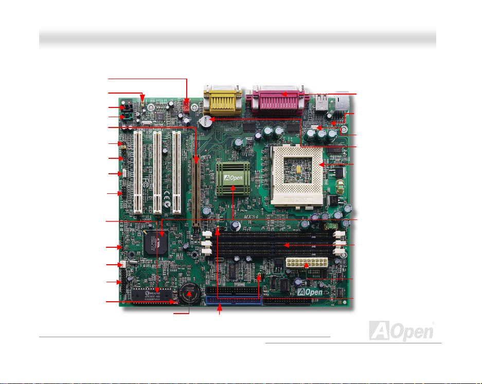
MMootthheerrbbooaarrdd MMaapp
Battery-less &
long-life Design
ATA/33/66 IDE
Suspend to HDD
(ATA/100 for optional)
10
FDD Connector
PC99 Back Pane l
Resettable Fuse
CPU Fan Connector
System Voltage & Fan Monitoring
Buzzer
Socket370 CPU with Vo ltage and
Frequency Auto-detection
supports Intel
& Celeron™ 300MHz~1GHz+ CPU
CPU Jumper-less Design
Over-current Protection
Thermal Protection
VIA 694X Chipset
Support 133MHz FSB Clock
168-pin DIMM Socket x3
suppo rts PC10 0/133 SDRAM
u
to 1.5GB
TX Power Connector
AC Power Auto Recovery
JP23/JP29
FSB/PCI Clock Ratio
®
Pentium® III
Page 11
MMXX334
4
OOn
n
iinne
e
MMaan
n
a
a
l
l
u
u
ll
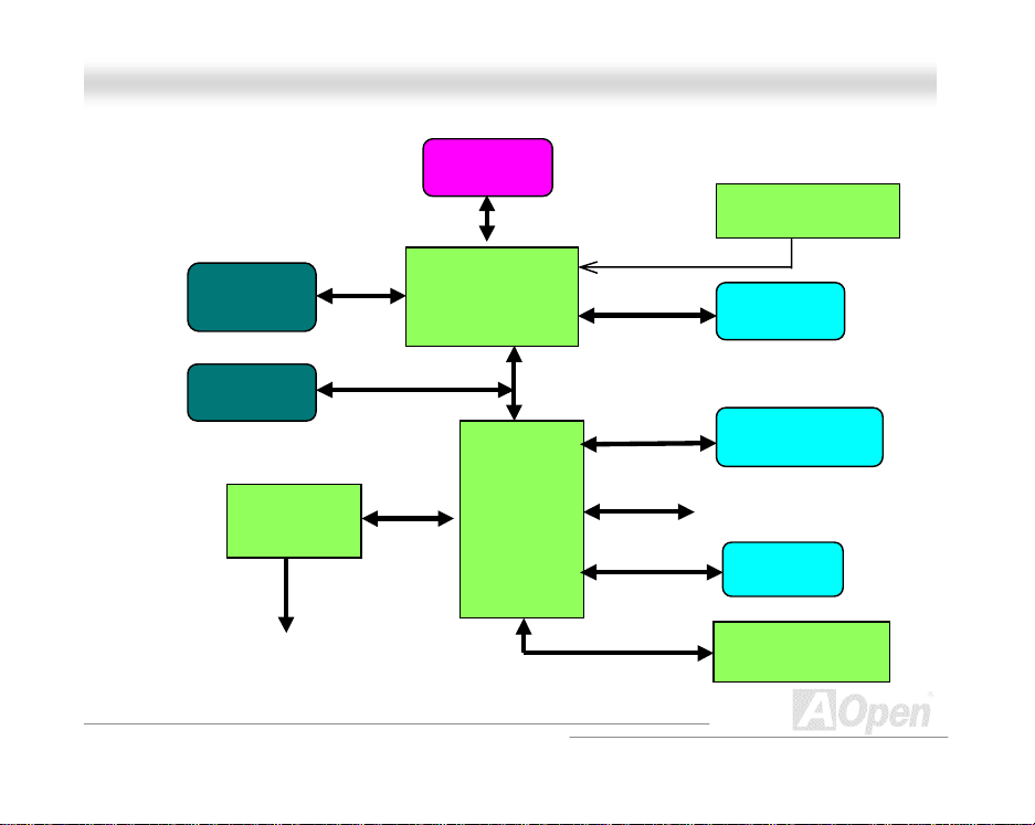
BBlloocckk DDiiaaggrraamm
AGP Card
4X mode
AGP Bus
PCI Card
Audio
CODEC
MIC, Line -i n
and Speaker
PCI Bus
AC97 Link
CPU
66/100/133MHz FSB
Nort h Br idge
VIA 694X
South
Bridge
VIA 686A
(686B for
optional)
11
66/100/133
Memory Bus
ATA 66/100
IDE Bus
ISA Bus
Clock Generator
DIMM
HDD/CDROM
USB, Serial port, Printer and
PS2 KB/Mouse
Floppy
BIOS Flash ROM
Page 12

MMXX334
4
OOn
n
iinne
e
MMaan
n
a
a
l
l
u
u
ll
HHaarrddwwaarree
This chapter describes jumpers, connectors and hardware devices of this motherboard.
Note: Electros tatic d ischarge (ESD) c an dama ge your pr ocessor, d isk
drives, ex pa nsion boar ds , an d other comp on ent s . Always observe t he
following prec autions before you install a system component.
1.Do not remove a co mponent fro m its protect ive packag ing until you
are ready to ins t a ll it.
2.Wear a wr ist grou nd stra p and attac h it to a met al part of th e syst em
unit before handling a component. If a wrist strap is not available,
maintain contact with the system unit throughout any procedure
requiring ESD protection.
12
Page 13
MMXX334
4
OOn
n
iinne
e
MMaan
n
a
a
123
l
l
u
u
ll
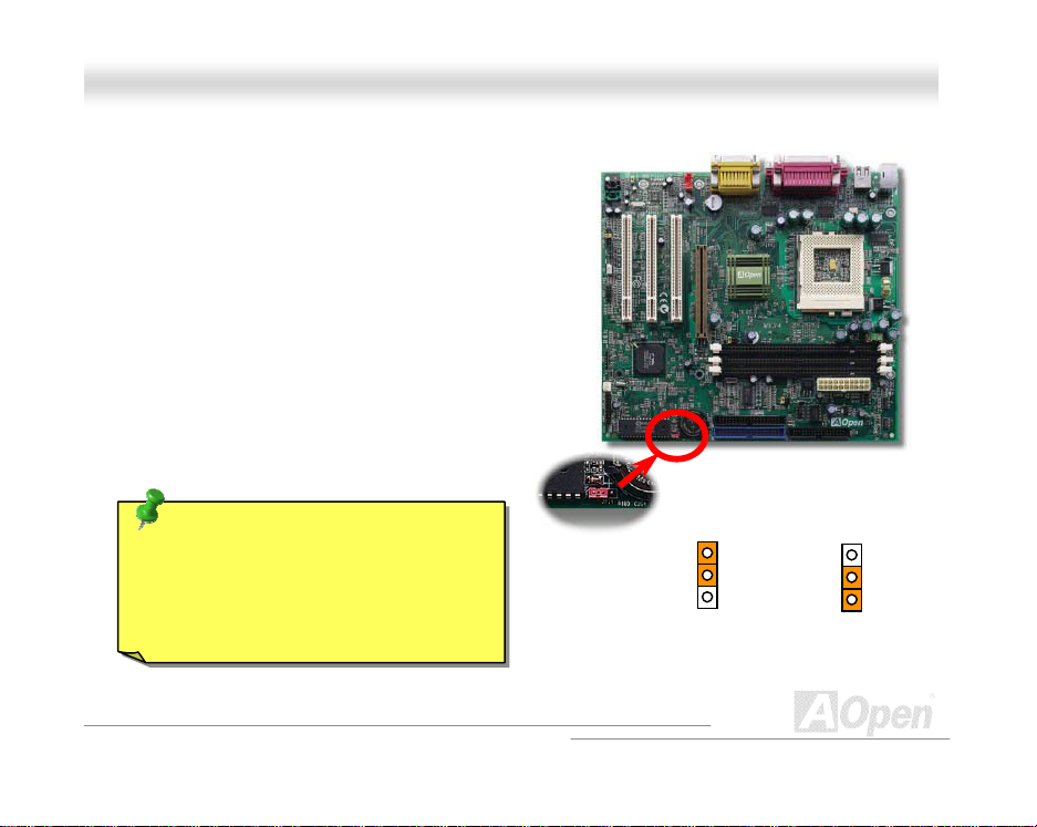
JJPP1144 CClleeaarr CCMMOOSS
You can clear CMOS to restore sy stem default setting. To
clear the CMOS, follow the procedure below.
1. Turn off the syst em an d un plug the AC power.
2. Remove ATX power cable from connector PWR2.
3. Locate JP14 and short pins 2-3 for a few seconds.
4. Return JP14 to its normal setting by shorting pins 1-2.
5. Connect ATX power cable back to connector PWR2.
Tip: When should I Clear CMOS?
1. Boot fail because of overclocking…
2. Forget password…
3. Troubleshooting…
13
1
3
Normal Operation
(default)
Clear CMOS
Page 14
MMXX334
4
OOn
n
iinne
e
MMaan
n
a
a
l
l
u
u
ll
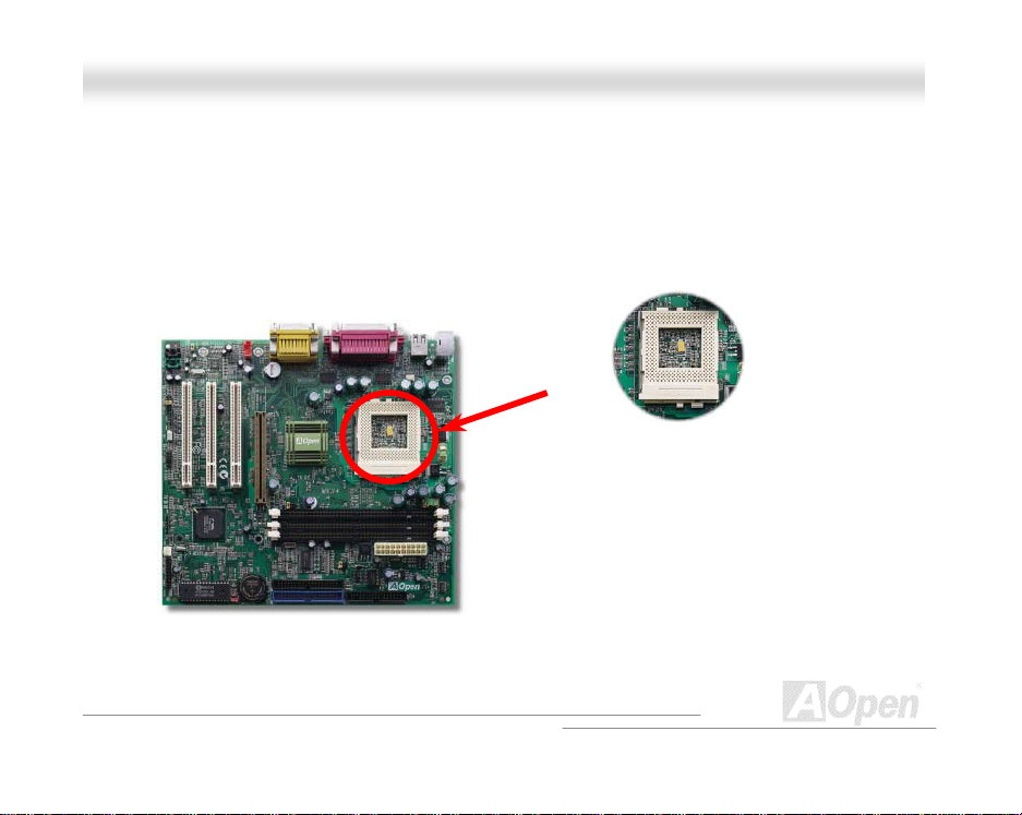
CCPPUU SSoocckkeett
This motherboard supports Celeron, and Pentium III FC-PGA Socket370 CPU. Be careful of CPU
orientation when you pug it int o CPU socket.
14
Page 15
MMXX334
4
OOn
n
iinne
e
MMaan
n
a
a
l
l
u
u
ll
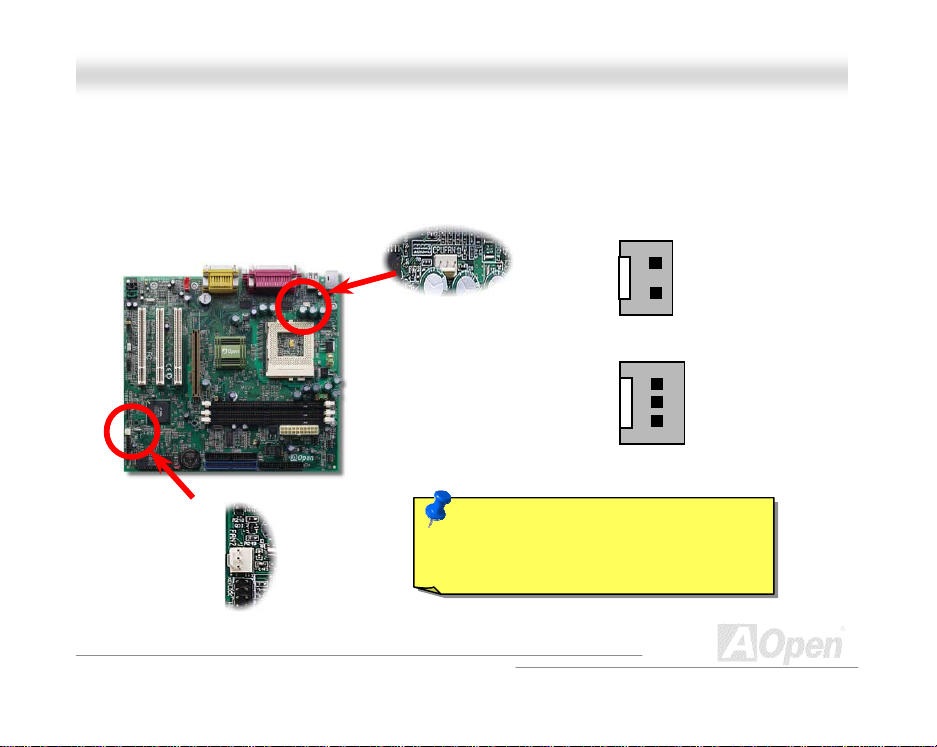
CCPPUU FFaann aanndd HHoouussiinngg FFaann CCoonnnneeccttoorr
Plug in the CPU fan cable to the 3-pin CPUFAN connector. If you have other housing fan, you can
also plug it on FAN connector.
Note: Some CPU fans do not have
sensor pin, so that cannot support fan
monitoring.
15
GND
+12V
GND
+12V
SENSOR
Page 16
MMXX334
4
OOn
n
iinne
e
MMaan
n
a
a
l
l
u
u
ll
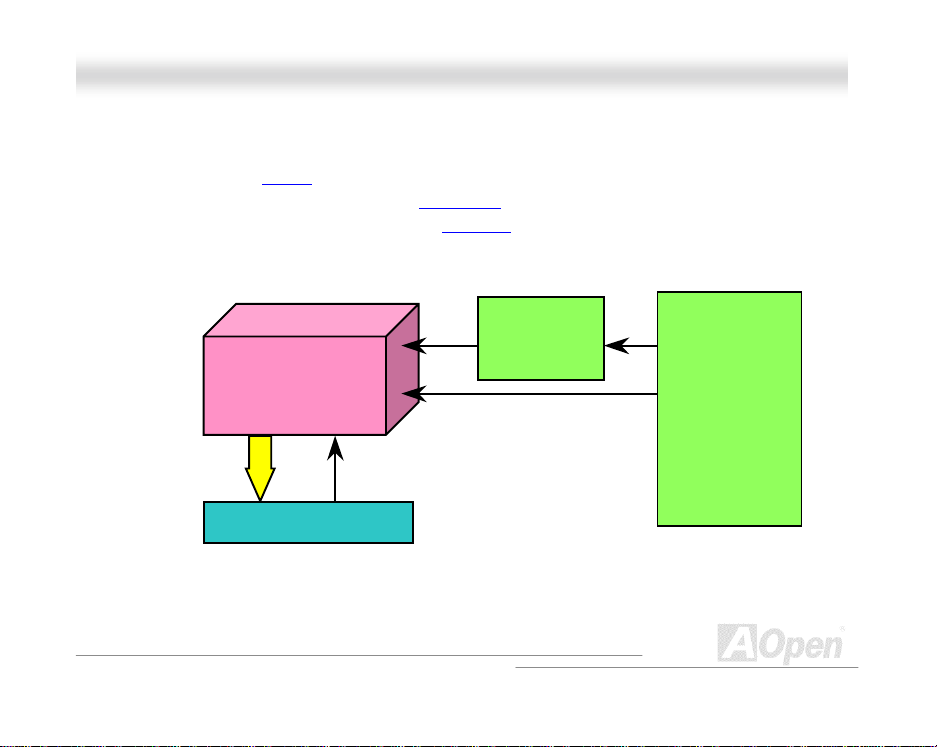
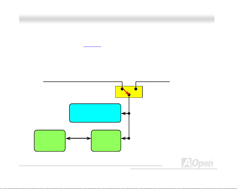
CCPPUU JJuummppeerr--lleessss DDeessiiggnn
CPU VID signal and SMbus clock generator provide CPU voltage auto-detection and allows the
user to set the CPU frequency through the BIOS setup
The correct CPU information is saved into the EEPROM
disad vant ag es of t h e Pent i u m based jumper-less desig ns are eliminated. There will be no worry of
wrong CPU voltage detection and no need to re-open the housing in case of CMOS battery loss.
CPU VID Signal
Pentium II/III &
Celeron CPU
CPU voltage
Power Regulator
(A ut omatically g en er at es CPU voltage)
, therefore no jumpers or s wi tc h es are used.
. With these t echn ol ogi es, th e
Clock
Generator
CPU Freq. Ratio
16
BIOS
Controlled
Circuit
Page 17
MMXX334
4
OOn
n
iinne
e
MMaan
n
a
a
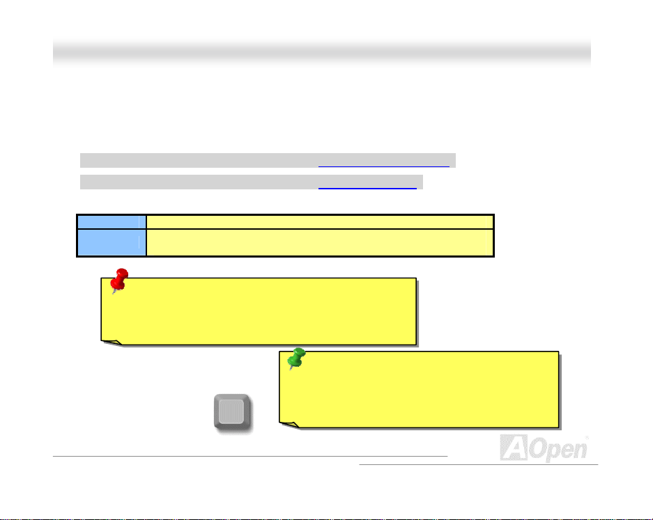
SSeettttiinngg CCPPUU FFrreeqquueennccy
This motherboard is CPU jumper-less design, you can set CPU frequency through the BIOS setup,
no jump ers or s witches are need ed .
BIO S Setup > C hipset Features Setup > CPU Clock Frequenc y
BIO S Setup > C hipset Features Setup > CPU Clock Ratio
CPU Ratio 1.5x, 2x, 2.5x, 3x, 3.5x, 4x, 4.5x, 5x, 5.5x, 6x, 6.5x, 7x, 7.5x, and 8x
CPU FSB
y
66.8, 75, 83.3, 100, 103, 105, 110 , 112, 115, 120, 124, 13 3,
140, and 15 0 MH z .
Warning: VIA 694X chipset supports maximum
133MHz FSB and 66MHz AGP clock, higher clock
setting may cause serious system damage.
Tip: If your syst em hangs o r fails to boot
because of overclocking, simply use <Home>
Home
key to restore the default setting (233MHz).
l
l
u
u
ll
17
Page 18
MMXX334
4
OOn
n
iinne
e
MMaan
n
a
a
Core Frequency = CPU FSB Clock * CPU Ratio
CPU CPU Core Frequency FSB Clock Ratio
CELERON 300A 300MHz 66MHz 4.5x
CELERON 600 600MHz 66MHz 9x
CELERON 700 700MHz 66MHz 10.5x
CELERON 800 800MHz 100MHz 8x
CELERON 850 850MHz 100MHz 8.5x
Pentium!!! 700E 700MHz 100MHZ 7x
Pentium!!! 750E 750MHz 100MHZ 7.5x
Pentium!!! 800E 800MHz 100MHZ 8x
Pentium!!! 850E 850MHz 100MHZ 8.5x
Pentium!!! 733EB 733MHz 133MHZ 5.5x
Pentium!!! 866EB 866MHz 133MHZ 6.5x
Pentium!!! 933EB 866MHz 133MHZ 7x
Pentium !!! 1G 1GHz 133MHZ 7.5x
Pentium !!! 1.13G 1.13GHz 133MHz 8.5
l
l
u
u
ll
18
Page 19
MMXX334
4
OOn
n
iinne
e
MMaan
n
a
a
(
X
(
X
(
(
l
l
u
u
ll
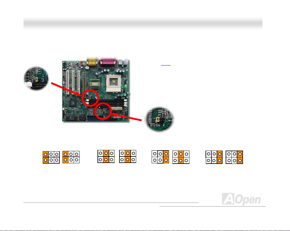
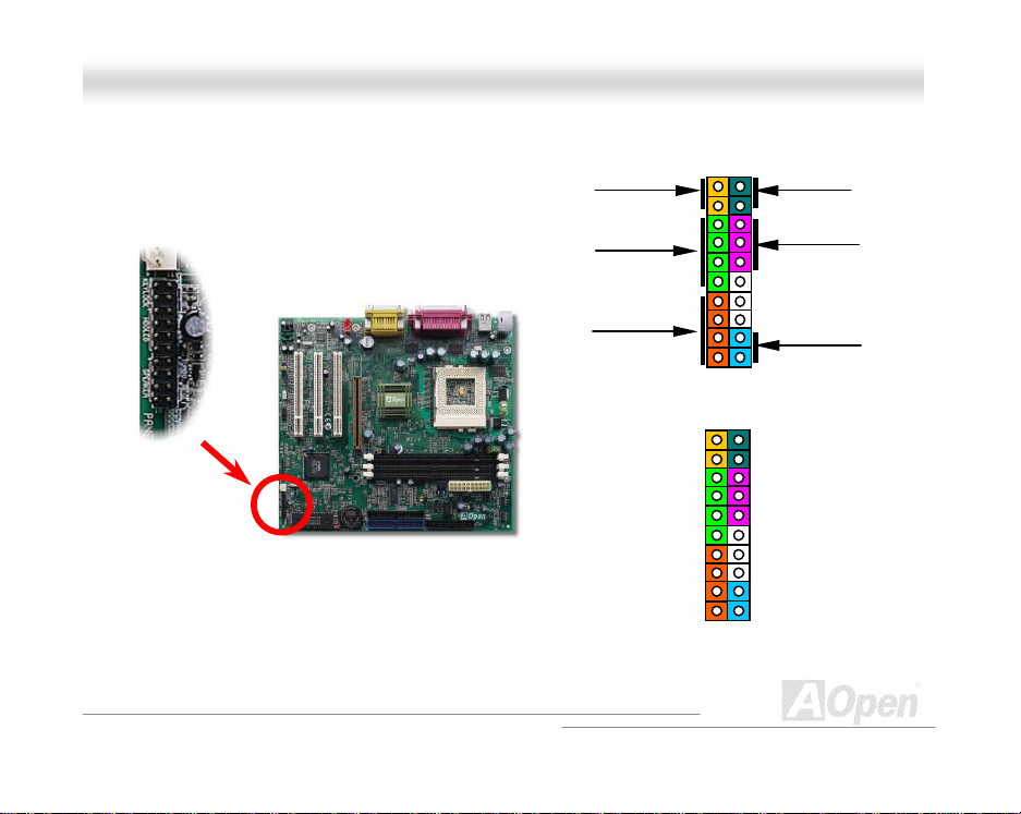
JJPP2299//JJPP2233 FFSSBB//PPCCII CClloocckk RRaattiioo
JP29
JP29 JP23
1
2
Auto
default)
5
6
JP29 JP23
4X
133~150MHz)
This jumper is used to specify the relationship of
PCI and FSB
not overclockers, we recommend to set at the
default setting. For example, you must set JP29 to
“5-6” and JP23 t o “3-4” if you want to overclock a
66MHz FSB clock CPU to 100MHz or higher.
JP29 JP23 JP29 JP23
100~124MHz)
19
cloc k. Gen erally sp eaking, if you are
JP23
3
2
66~83MHz)
Page 20
MMXX334
4
OOn
n
iinne
e
MMaan
n
a
a
PCI Clock = CPU FSB Clock / Clock Ratio
AGP Clock = PCI Clock x 2
Clock Ratio CPU (Host) PCI AGP Memory
2X 66 33 66 PCI x2 or x3
3X 100 33 66 PCI x2 or x3 or x4
3X, overc l oc ki ng 112 37.3 74.6 PCI x2 or x3 or x4
4X 133 33 66 PCI x3 or x4
4X, overc l oc ki ng 155 38.75 77.5 PCI x3 or x4
Warning: VIA 694X chipset supports maximum 133MHz FSB and
66MHz AGP clock, higher clock setting may cause serious system
damage.
l
l
u
u
ll
20
Page 21
MMXX334
4
OOn
n
iinne
e
MMaan
n
a
a
l
l
u
u
ll
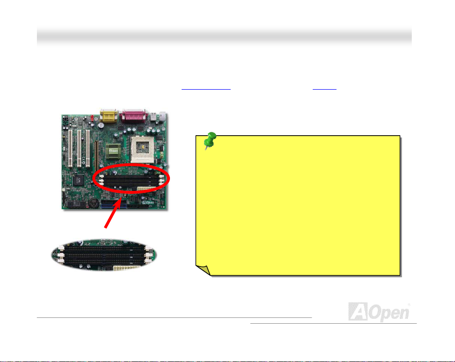
DDIIMMMM SSoocckkeett
This moth erb oard has three 1 68- pin DIMM socke ts that allow you to install PC133 memory up to
1.5GB. Only SDRAM is supported.
Pin 1
Tip: The driving capability of new generation chipset
is limited due to the lack of a memory buffer (to
improve performance). This makes DRAM chip count
an important factor to take into consideration when
you install DIMMs. Unfortunately, there is no way that
the BIOS can identify the correct chip count, you
need to calculate the chip count by yourself. The
DIMM1
DIMM2
DIMM3
simple rule is: By visual inspection, use only
DIMMs which are less than 18 ch ips..
21
Page 22
MMXX334
4
OOn
n
iinne
e
MMaan
n
a
a
DIMM can be single side or double side, it has 64 bit data and 2 or 4 clock signals. We strongly
recommend choosing 4-clock SDRAM for its reliability
Tip: To identify 2-clock and 4-clock DIMM, you may
check if there are traces connected to the golden
finger pins 79 and 163 of the SDRAM . If th ere are
traces, the SDR AM is probably 4-clock; otherwise, it
is 2-cloc k .
Tip: To identify single-side or double-side DIMM,
check golden finger pin 114 and pin 129. If there are
traces connected to pin 114 and pin 129, the DIMM
is probably double-side; otherwise, it is single-side.
l
l
u
u
ll
22
Page 23
MMXX334
4
OOn
n
iinne
e
MMaan
n
a
a
A
l
l
u
u
ll
FFrroonntt PPaanneell CCoonnnneeccttoorr
23
Keylock
IDE LED
Speaker
KEYLOCK
IDE LED
IDE LED
SPEAKER
+
+
+
GND
+5V
+5V
+5V
GND
NC
1
+
+
+
1
SPWR
GND
ACPI & PWR LED
GND
+5V
NC
+5V
GND
RESET
GND
SPWR
CPI &
Power LED
Reset
Page 24
MMXX334
4
OOn
n
iinne
e
MMaan
n
a
a
Attach t he pow er LED , k eyloc k, sp eak er, and res et s witc h c onnec t ors t o th e c orresp on ding pins . If
you enable Power Management > Susp en d Mode
flashing while the system is in suspend mode.
Locate the power switch cable from your ATX housing. It is 2-pin female connector from the housing
front panel. Plug this connector to the soft-power switch connector marked SPWR.
in BIOS Setup, the ACPI & Power LED will keep
Suspend Type ACPI LED
Power on Suspend (S1) Fla shing for every second
Suspend to RAM (S3) Flashin g for every 4 seconds
l
l
u
u
ll
24
Page 25
MMXX334
4
OOn
n
iinne
e
MMaan
n
a
a
l
l
u
u
ll
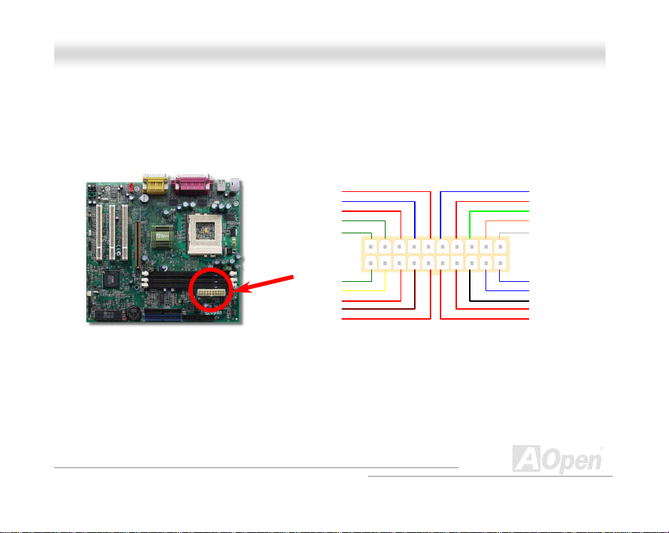
AATTXX PPoowweerr CCoonnnneeccttoorr
The ATX power supply uses 20-pin connector shown belo w. Make sure you plug in the right
direction.
COM
+5V
COM
+3.3V
+3.3V
+5V
COM
PW-OK
5VSB
+12V
+3.3V
-12V
COM
PS-ON
COM
+5V
+5V
-5V
COM
COM
25
Page 26

MMXX334
4
OOn
n
iinne
e
MMaan
n
a
a
l
l
u
u
ll
AACC PPoowweerr AAuuttoo RReeccoovveerryy
A tradition al ATX system should r emain at power off stage when AC p ower res umes fr om power
failure. T h is d es ign is inconvenient for a network s erv er or workstation, without an U PS, that n eeds
to keep p ower-on. This m ot h erb oard implem ents an AC Power A ut o Recovery func t i on to solve this
problem . I f BIOS Set up > Power m an ag em ent > AC PW R Auto R ecov ery is set to “On” the system
will autom at ically power- on af t er AC power r esu m es .
26
Page 27
MMXX334
4
OOn
n
iinne
e
MMaan
n
a
a
l
l
u
u
ll
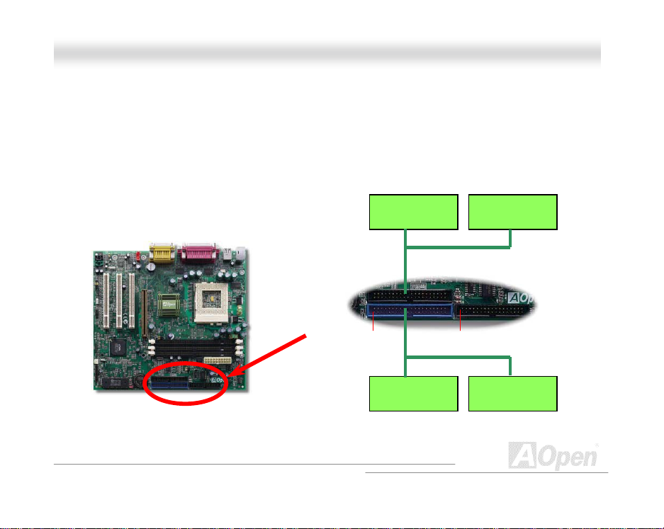
IIDDEE aanndd FFllooppppyy CCoonnnneeccttoorr
Connect 34-pin floppy cable and 40-pin IDE cable to floppy connector FDC and IDE connector The
blue connector is IDE1 for clear identification. Be careful of the pin1 orientation. Wrong orientation
ma y cause system damage.
IDE2 (Secondary)
IDE1 (Primary)
Pin 1
27
Slave (4 th)
Master (3rd)
FDC
Pin 1
Master (1st)Slave (2 nd)
Page 28
MMXX334
4
OOn
n
iinne
e
MMaan
n
a
a
IDE1 is also k nown as th e primar y channel and IDE2 as th e second ary c hannel. Each chan nel
supports two IDE devices that make a total of four devices. In order to work together, the two
devices on each channel must be set differently to master and s lav e mod e. E ither on e can b e th e
hard disk or the CDROM. The setting as master or slave mode d epends on the jumper on your IDE
device, so please refer to your hard disk and CDROM manual accordingly.
Warning: Th e sp ecification of the ID E ca ble is a
maximu m of 46cm (18 inches) , make sure your cable
does not exceed this length.
Tip: For better signal quality, it is recommended t o
set the far end side device to m as ter m ode and
follow the suggested sequence to install your new
device. Please refer to above di agram.
l
l
u
u
ll
28
Page 29
MMXX334
4
OOn
n
iinne
e
MMaan
n
a
a
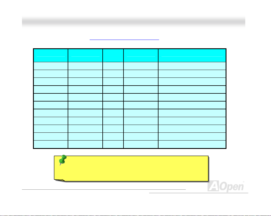
This motherboar d supports ATA 66 IDE (ATA/100 for optional). Following table lists the transfer rate
of IDE PIO and D M A modes. The IDE bus is 16- b it, which means ev e ry trans fer is two bytes.
Mode Clock Period Clock
PIO mode 0 30ns 20 600ns (1/600ns) x 2byte = 3.3MB/s
PIO mode 1 30ns 13 383ns (1/383ns) x 2byte = 5.2MB/s
PIO mode 2 30ns 8 240ns (1/240ns) x 2byte = 8.3MB/s
PIO mode 3 30ns 6 180ns (1/180ns) x 2byte = 11.1MB/s
PIO mode 4 30ns 4 120ns (1/120ns) x 2byte = 16.6MB/s
DMA mode 0 30ns 16 480ns (1/480ns) x 2byte = 4.16MB/s
DMA mode 1 30ns 5 150ns (1/150ns) x 2byte = 13.3MB/s
DMA mode 2 30ns 4 120ns (1/120ns) x 2byte = 16.6MB/s
UDMA/33 30ns 4 120ns (1/120ns) x 2byte x2 = 33MB/s
UDMA/66 30ns 2 60ns (1/60ns ) x 2byte x2 = 66MB /s
UDMA/100 20ns 2 40ns (1/40ns) x 2byte x2 = 100MB/s
Cycle Time Data Transfer Rate
Count
Tip: To ac h iev e th e best perform anc e of U ltr a DMA 66 /1 00 h ar d
disks, a special 80-wires IDE cable for Ultra DMA66/100 is
requir ed..
l
l
u
u
ll
29
Page 30
MMXX334
4
OOn
n
iinne
e
MMaan
n
a
a
4
5
6
l
l
u
u
ll
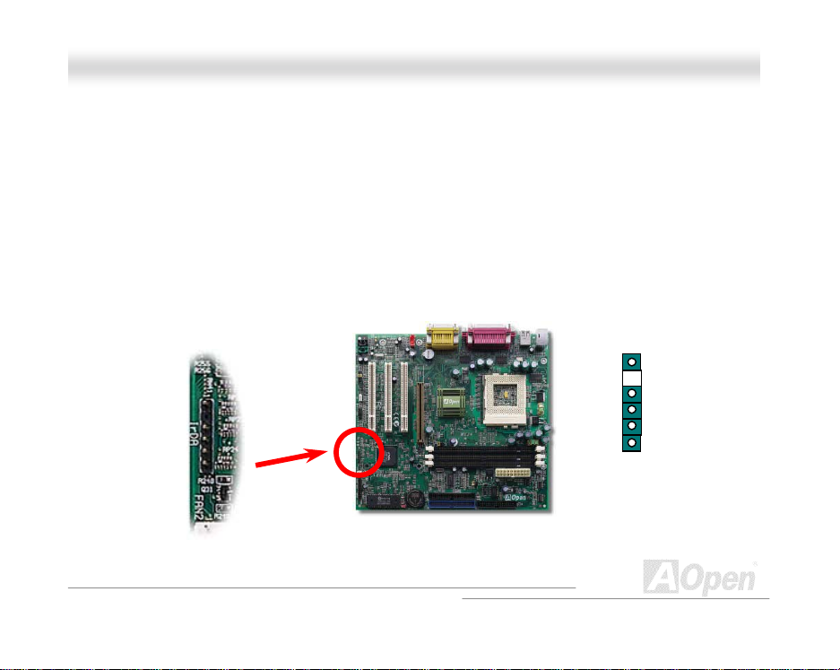
IIrrDDAA CCoonnnneeccttoorr
The IrD A connector can b e configur ed to sup port w ireless infrared modul e, with th is modu le and
applic ati on software s uc h as L aplink or Windows 95 D irect Cabl e Connection, t h e user can tr ans fer
files to or from laptops, notebooks, PDA devices and printers. This connector supports HPSIR
(115.2Kbps, 2 m eters ) an d ASK-IR (56Kbps).
Install th e infrared m odule onto the IrDA connector and enab le the infrared function from BIO S
Setup, U ART mode s elect , mak e sure t o have th e correct orientati on when you plug in the IrDA
connector.
Pin 1
+5V
1
NC
2
IRRX
3
GND
IRTX
NC
30
Page 31

MMXX334
4
OOn
n
iinne
e
MMaan
n
a
a
l
l
u
u
ll
WWOOMM ((ZZeerroo VVoollttaaggee WWaakkee oonn MMooddeemm))
This motherboard implements s pecial circuit to support W ake On Modem, both Internal modem
card and ext ernal box mod em are support ed. Si nce Internal m od em c ar d c ons u m es n o pow er when
system power is off, it is recomm end ed to use an in t er n al m odem. To use inter n al modem, connect
4-pin cable from RING connector of mod em card to the WOM connec tor on the motherb oard.
1
+5V Standby
NC
RING
GND
Pin 1
31
Page 32

MMXX334
4
OOn
n
iinne
e
MMaan
n
a
a
WWOOMM bbyy EExxtteerrnnaall BBOOXX MMooddeem
Traditional Green PC suspend mode does not really turn off the system power supply, it uses
exter nal box modem to trigger MB COM port and resume back to active.
COM port
Motherboard
m
Box Modem
TEL Line
l
l
u
u
ll
32
Page 33

MMXX334
4
OOn
n
iinne
e
MMaan
n
a
a
WWOOMM bbyy IInntteerrnnaall MMooddeemm CCaarrd
With the help of the ATX soft power On/Off, it is possible to have a system totally power off, and
wakeup to aut omatic ally ans wer a phone call as an ans wering machin e or to sen d/receive a f ax.
You may identify wheth er or n ot your syst em is in true p ower off mod e b y c h ec k in g to see if the fan
of your p ow er suppl y is off. Both an ext er n al b ox modem and an i nternal mod em card can b e used
to support Modem Wake Up, but if you us e an external modem, you have to leave your box modem
on.
Modem Card
Motherboard
l
l
d
TEL Line
With AOpen Motherboard plus AOpen Modem Card,
the po wer can be totally off
.
u
u
ll
33
Page 34

MMXX334
4
OOn
n
iinne
e
MMaan
n
a
a
l
l
u
u
ll
WWOOLL ((WWaakkee oonn LLAANN))
This f eature is ver y similar as Wake On Modem, but it goes throu gh local ar ea network. To us e
Wake On LAN func tion , you mus t h ave a net work c ard with chips et that su pports t his f eat ur e, an d
connect a cable from LAN card to motherboard WOL connector. The system identification
inform ation (pr obabl y IP address) is stored on net wor k card and bec ause ther e is a lot of traffic on
the Ethernet, you need to install a network management software, such as ADM, for the checking of
how to wak e up th e system . Note th at, at least 60 0mA ATX standby c urrent is requir ed to sup port
the LAN card for this function.
+5V Standby
GND
LID
Pin 1
34
Page 35

MMXX334
4
OOn
n
iinne
e
MMaan
n
a
a
LAN Card
Motherboard
Ethernet
l
l
u
u
ll
35
Page 36

MMXX334
4
OOn
n
iinne
e
MMaan
n
a
a
l
l
u
u
ll
44XX AAGGPP ((AAcccceelleerraatteedd GGrraapphhiicc PPoorrtt))
This motherboard supports 4X AGP. AGP is a bus int erface designed for high-perf ormance 3D
graphic and su ppor ts onl y mem ory r ead/ writ e oper ati on. O ne mot her board can on l y have one A GP
slot. 2X AGP us es b ot h ris ing and falling ed g e of t h e 66MHz clock, th e data trans f er r ate is 66MHz
x 4 bytes x 2 = 528MB/s. 4X AGP is sti ll using 66MHz AGP clock but the it has 4 d ata transf ers
within one 66MHz clock cycle, so that the data transfer rate is 66MHz x 4 bytes x 4 = 1056MB/s.
36
Page 37

MMXX334
4
OOn
n
iinne
e
MMaan
n
a
a
l
l
u
u
ll
PPCC9999 CCoolloorr CCooddeedd BBaacckk PPaanneell
The on boar d I/O devic es ar e PS /2 K eyb oar d, P S/2 M ous e, s erial p orts C OM 1 and CO M2, Pr int er,
four USB
panel of the housing.
, AC97 sound and Gam e port. T he view angle of drawing shown here is fr om the back
PS/2 Mouse
Connector
USB Port
PS/2
Keyboard
Connector
Speaker: To Extern al Speaker, Earphone or Amplifi er.
Line-In: From signal source such as CD/Tape player.
MIC: From Microphone
COM 1 Port COM 2 Port
37
MIDI/Game
Port
MIC-In
Line-In
Speaker Out
Page 38

MMXX334
4
OOn
n
iinne
e
MMaan
n
a
a
l
l
u
u
ll
SSuuppppoorrtt 44 UUSSBB PPoorrttss
This motherboard supports four USB ports. Two of them are on back panel connector, the other two
are on the left-bottom area of this motherboard. With proper cable, you can connect them to front
panel.
D2-
D2+
GND
NC
+5V
Pin 1
1 2
D3D3+
GND
NC
+5V
9 10
38
Page 39

MMXX334
4
OOn
n
iinne
e
MMaan
n
a
a
l
l
u
u
ll
JJPP1122 EEnnaabbllee//DDiissaabbllee OOnnbbooaarrdd SSoouunndd
This m otherboar d has AC97 s ound onboar d. JP12 is used to en able or d isable on board AD1 885
CODEC
chip. If you select Disable, you can use your preferred PCI sound card.
Enable
1
2
3
Disable
1
2
3
39
Page 40

MMXX334
4
OOn
n
iinne
e
MMaan
n
a
a
l
l
u
u
ll
CCDD AAuuddiioo CCoonnnneeccttoorr
This CD-IN is used to connect CD Audio cable from CDROM or DVD drive to onboard sound.
CD-IN
40
LR
GND
Page 41

MMXX334
4
OOn
n
iinne
e
MMaan
n
a
a
l
l
u
u
ll
AAUUXX--IINN CCoonnnneeccttoorr
The AUX-IN connector is used to connect MPEG Audio cable from MPEG card to onboard
AUX-IN
LR
GND
41
Page 42

MMXX334
4
OOn
n
iinne
e
MMaan
n
a
a
)
l
l
u
u
ll
MMooddeemm AAuuddiioo CCoonnnneeccttoorr
This c onnector is us ed to conn ect Mono I n/Mic Out c able from i nternal m odem card t o onboard
sound cir cuit. The p in 1-2 is M ono In, and th e pin 3-4 is Mic Out. Please not e that ther e is no
standard for this kind of connector yet, only some internal modem cards implement this connector.
Pin 1
42
Mono-In (T o Modem)
GND
GND
MIC-Out (From Modem
Page 43

MMXX334
4
OOn
n
iinne
e
MMaan
n
a
a
j
l
l
u
u
ll
FFrroonntt AAuuddiioo CCoonnnneeccttoorr
If the housin g has been desi gn with an audi o port on the front pan el, you’ll b e able to connect
onboard audi o t o front p an el throu gh t his c onn ector. B y the way, pleas e r emov e the ju mp er cap
from the F ront P anel Au di o Conn ect or b efor e you c onn ect th e c abl e. Do not rem ove th is yellow
umper cap if housing without an audio port on the front panel.
Pin 1
1 2
MIC_IN2
VREFOUT
PHONE_R
NC
PHONE_L
GND
+5V
NC
NC
9 10
43
Page 44
MMXX334
4
OOn
n
iinne
e
MMaan
n
a
a
l
l
u
u
ll
BBaatttteerryy--lleessss aanndd LLoonngg LLiiffee DDeessiiggnn
This Motherboard implements EEPROM and a special circuit that allows you to save your current
CPU and CMOS Setup conf ig urations with out the need of a batter y. The RTC (real ti m e cl oc k) c an
also keep r un ni ng as long as the power c ord is plugged. If you l os e your C MOS data by accid ent,
you can just reload the CMOS configurations from EEPROM and the system will recover as usual.
EEPROM CMOS
Auto Switch
RTC real time clock
00:00:00
Backup by EEPROM
44
Battery ATX standby power
Auto swit ch to ATX standby
po wer as long as AC p o wer
line is plugged. This smart
design increases batt ery life
if you still pl ug b att ery on
motherboard.
Page 45

MMXX334
4
OOn
n
iinne
e
MMaan
n
a
a
l
l
u
u
ll
OOvveerr--ccuurrrreenntt PPrrootteeccttiioonn
The O ver C urr ent Pr otect ion w as very popu l ar im plem ent ed on ATX 3.3V /5V /12V s witc hin g p ower
suppl y. However, th e n ew g en eration CPU uses different volt ag e t h at has r eg ul ator to transfer 5V to
CPU voltag e (f or examp l e, 2.0V) , and m akes 5V over curren t pr otect i on usel ess. Th is m other boar d
with switching regulator onboard support CPU over-current protection, in conjunction with
3.3V/5V/12V power supply provide the full line over-current protection.
ATX
Switching
Power
Supply
12V (Protected by power supply)
3.3V (Protected by power supply)
5V (Protected by power supply)
Onboard
Power
Regulator
Over-Current
Protection
Circuit
45
CPU Core Vol t age
Page 46

MMXX334
4
OOn
n
iinne
e
MMaan
n
a
a
Note: Alth ough we have implemen ted pro tection circu it try t o prevent
any human operating mistake, there is still certain risk that CPU,
memory, HDD, add-on cards installed on this motherboard may be
damaged because of component failure, human operating error or
unknown nature reason. AOpen cannot guaranty the protection
circuit will always work perfectly.
l
l
u
u
ll
46
Page 47

MMXX334
4
OOn
n
iinne
e
MMaan
n
a
a
l
l
u
u
ll
HHaarrddwwaarree MMoonniittoorriinngg
This motherboard implements a hardware monitoring system. As you turn on your system, this
smart design will continue to monitor your system’s working voltage, fan status and CPU
temper ature. If any of thes e system ’s status go wr ong, th ere will b e an alarm th rough th e AOpen
Hardware Monitoring Utility
Fan
CPU
Power
to warn the user.
Fan Speed
CPU Temperature
CPU Voltage
System Voltage
47
Detection
Circuit
AOpen
HWMON
Utility
Page 48

MMXX334
4
OOn
n
iinne
e
MMaan
n
a
a
l
l
u
u
ll
RReesseettttaabbllee FFuussee
Tradition al mot herboar d has fus e for K eyboar d and USB port to pr event over-c urrent or sh ortage.
These f uses are soldered onboard that wh en it is broken ( di d th e job to protect m ot h erb oard), us er
still cannot replace it and the motherboard is still malfunction.
With exp ensive R esettabl e Fuse, t he moth erboard can bac k to norm al funct ion after f use did t he
protection job.
48
Page 49

MMXX334
4
OOn
n
iinne
e
MMaan
n
a
a
l
l
u
u
ll
YYeeaarr 22000000 ((YY22KK))
Y2K is bas ically a problem of the identific ation of year cod e. To save storage space, tr aditional
softwar e uses onl y two digits f or year identif icati on. For exam ple, 98 for 1998 and 99 f or 1999, but
00 will be confused with 1900 and 2000.
There is an RTC cir c u it ( Real Time C l oc k) in conjunc t i on with 12 8 b y tes of CMO S R A M d at a in t he
chipset of the motherboard. The RTC has only two digits and the CMOS has another 2 digits.
Unfortunately, this circuit’s behavior is like this 1997! 1998 ! 1999 ! 1900, th at means it may
have the Y2K pr oblem. Below is a diagr am of h ow applications w ork wi th the OS, BIOS and RTC. In
order to keep th e best c omp atibility in the PC i nd us t r y there is a rule that applic ations mus t call the
OS to get services and OS must call the BIOS, and then only BIOS is allowed to access the
hardwa re (RTC) d irectly.
49
Page 50

MMXX334
4
OOn
n
iinne
e
MMaan
n
a
a
App
)
)
l
l
u
u
ll
There is a Tick Routine (that goes live around every 50m sec) in the BIOS to keep record of
date/time information. In general the BIOS, this Tick Routine does not update the CMOS every time
because the CMOS is a very slow device which degrades system performance. The Tick Routine of
the AOpen BIOS has 4 digits for year c oding, as long as applic at ions and the operati ng system
follow t he rule to get date/t ime infor mation. Th ere will be no Y2K pr oblem (suc h as NSTL’s tes t
program) . But unfortu nately ag ain, we found some t est prog rams (s uch as C heckit 98) acc esses
RTC/CMOS directly. This motherboard has hardware Y2K checking and protection that
ensures risk free operation.
Operating System (such as Windows 98
BIOS (Tick Routine
RTC and CMOS data
lications
50
Page 51

MMXX334
4
OOn
n
iinne
e
MMaan
n
a
a
l
l
u
u
ll
11550000uuFF LLooww EESSRR CCaappaacciittoorr
The quality of low ESR capacitor (Low Equivalent Series Resistance) during high frequency
operation is very im p or t ant for stabil it y of CP U p ower. The location of wh ere to put thes e capacitors
is another know-how that requires experience and detail calculation.
Not only that, this motherboard implements Low ESR capacitors, which is much larger than
normal (1000uF) and provide better stability for CPU power.
51
Page 52

MMXX334
4
OOn
n
iinne
e
MMaan
n
a
a
Th e power ci rcu it of the C PU c ore vo ltage mu st b e chec ked t o en sure s yst em st ability f or h igh
speed CPU s (suc h as the new Pent ium III, or wh en overcl ocking). A typical C PU core voltage is
2.0V, so a good des ign shoul d control voltage bet ween 1.86 0V and 2.1 40V. That is, the trans ient
must b e bel ow 2 80 mV. Bel ow is a ti ming diagram captured b y a D ig it al Stor ag e Scope, it sh ows t h e
voltage transient is onl y 143mv even when maximum 18A curr ent is applied.
l
l
u
u
ll
52
Page 53

MMXX334
4
OOn
n
iinne
e
MMaan
n
a
a
l
l
u
u
ll
LLaayyoouutt ((FFrreeqquueennccyy IIssoollaattiioonn WWaallll))
Note: This diagram for example only, it may not be exactly
the same as this motherboard.
53
For high frequency operation, especially
overcl ocki ng, l ayou t is th e m ost i mp ortant
factor to make sure chipset and CPU
working in s table c onditi on. T he la yout of
this motherboard implements AOpen’s
unique design called “ Frequency
Isolation Wall”. Separating each critical
portion of m oth er b oar d into regi ons wh ere
each r egi on operates in a same or s imilar
frequenc y r ange to avoid cross talk and
frequency interference between each
region’s operations and condition. The
trace lengt h and rout e must be calcul ated
carefully. For example, the clock trace
must be equal length (not necess arily as
short as possible) so that clock skew will
be controlled within few a pico second
12
Sec)
(1/10
Page 54

MMXX334
4
OOn
n
iinne
e
MMaan
n
a
a
l
l
u
u
ll
DDrriivveerr aanndd UUttiilliittyy
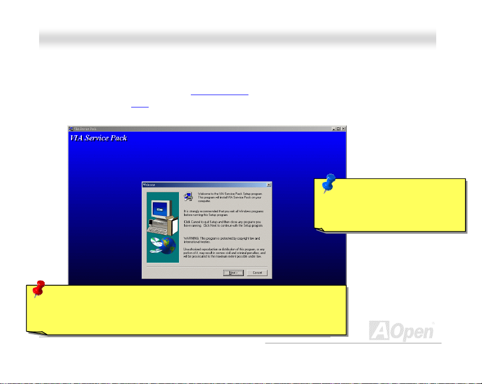
There ar e mother board drivers and utilities inclu ded in AOpen Bon us CD disc. You don’t n eed to
install all of th em in order to boot your s ystem . But after you finis h the hardwar e install ation, you
have t o ins t all you r op er ation s ys t em firs t (s uc h as W ind ows 98) b efor e you c an i nst all any dr i vers
or utilities. Please refer to your operation system’s installation guide.
Note: Please follow recommended procedure to install
Windows 95
and Windows 98.
54
Page 55

MMXX334
4
OOn
n
iinne
e
MMaan
n
a
a
l
l
u
u
ll
AAuuttoorruunn MMeennuu ffrroomm BBoonnuuss CCDD DDiisscc
You can use the aut orun menu of Bonus CD disc. Choos e t h e util ity and driver and s elec t m od el
name.
55
Page 56

MMXX334
4
OOn
n
iinne
e
MMaan
n
a
a
l
l
u
u
ll
IInnssttaalllliinngg WWiinnddoowwss 9955
1. First, d on’ t ins tall any add-on c ard except AGP card.
2. Install Windows 95 OSR 2 v2 . 1, 12 12 or 12 14 ver s i on and later with U SB su pp or t . Ot h erwise,
you need t o inst all U SBSUPP.EXE.
3. Install the VIA 4 in 1 driver
driver and V IA regis tr y (I N F) program.
4. Finall y, Install ot h er add-on cards and th eir drivers.
, which includes VIA AGP Vxd driver, VIA ATAPI Vendor Support
56
Page 57

MMXX334
4
OOn
n
iinne
e
MMaan
n
a
a
l
l
u
u
ll
IInnssttaalllliinngg WWiinnddoowwss 9988
1. First, d on’ t ins tall any add-on c ard except AGP card.
2. Enable U SB Contr oller in BIOS S etup > Ad vanced Ch ipset Feat ures > USB CO ntroller, to
make BIOS fully capable of controlling IRQ assignment.
3. Install Window 98 into your system.
4. Install the VIA 4 in 1 driv er
Vendor Supp ort dri ver an d VIA regis try (INF) program.
5. Finall y, Install ot h er add-on cards and th eir drivers.
, which includes VI A AGP Vxd driver, I RQ Routing, VIA ATAPI
57
Page 58

MMXX334
4
OOn
n
iinne
e
MMaan
n
a
a
l
l
u
u
ll
IInnssttaalllliinngg WWiinnddoowwss 9988 SSEE,, WWiinnddoowwss MMEE &&
WWiinnddoowwss22000000
If you ar e using W indows® 98 Sec ond Editi on, Windows® Millenn ium Edition or Wind ows® 2000,
you do not need t o inst all the 4-in- 1 driver as the IRQ Routin g Driver and th e ACPI R egistry ar e
already incorp orated into t he oper ating syst em. Us ers with W indows
Registry INF and AGP drivers by installing them individually.
Please refer to VIA Technologie s Inc.
http://www.via.com/
http://www.via.com/drivers/4in1420.exe
for latest v ers i on of 4 in 1 dr i ver:
58
®
98 SE may update the VIA
Page 59
MMXX334
4
OOn
n
iinne
e
MMaan
n
a
a
l
l
u
u
ll
IInnssttaalllliinngg VVIIAA 44 iinn 11 DDrriivveerr
You can install th e VI A 4 in 1 driver (IDE Bus mast er (For Windows NT use), VIA ATAPI Vendor
Support Driver, VIA AGP
from the Bonus Pack CD disc Autorun menu.
Warning: If you want to uninstall the VIA AGP Vxd driver, please remove the
AGP card driver first. Otherwise, the screen may go black at rebooting after the
un-installation.
, IRQ Routing Driver (For Windows 98 use), VIA Registry (INF) Driver)
59
Note: Instal ling this Bus Master
IDE driver may cause Suspend to
Hard Drive failure.
Page 60

MMXX334
4
OOn
n
iinne
e
MMaan
n
a
a
l
l
u
u
ll
IInnssttaalllliinngg OOnnbbooaarrdd SSoouunndd DDrriivveerr
If this motherboard comes with an AD 1885 AC97 CODEC, you can find the audio driver from the
Bonus Pac k CD dis c autorun menu.
60
Page 61

MMXX334
4
OOn
n
iinne
e
MMaan
n
a
a
l
l
u
u
ll
IInnssttaalllliinngg HHaarrddwwaarree MMoonniittoorriinngg UUttiilliittyy
You can install H ardw are Monit oring U tilit y to mon itor C PU tem peratur e, fans and s ystem voltage.
The hardw are monit ori ng func ti on is autom atic ally im plem ent ed by the BIOS and uti lit y softw are, no
hardw are ins t allation is needed .
61
Page 62

MMXX334
4
OOn
n
iinne
e
MMaan
n
a
a
l
l
u
u
ll
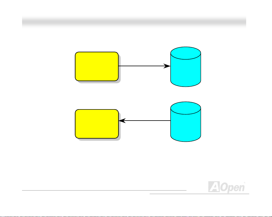
AACCPPII SSuussppeenndd ttoo HHaarrdd DDrriivvee
ACPI Suspen d to Hard Dri ve is basicall y controll ed by Windows operation s ystem. It s aves your
current work (system status, memory and screen image) into hard disk, and then the system can be
totally power off. Next time, when power is on, you can resume your original work directly from hard
disk withi n few sec onds wit hout go thr ough th e Windows bootin g process and run your applic ation
again. If you r mem ory is 64MB , norm ally, you n eed to res erve at least 64MB HDD s pace t o sav e
your memory image.
62
Page 63
MMXX334
4
OOn
n
iinne
e
MMaan
n
a
a
l
l
u
u
ll
When go into Suspend:
System
Image &
Status
When power-on next time:
System
Image &
Status
Save into
Restore w it hi n
seconds
63
Hard
Disk
Hard
Disk
Page 64

MMXX334
4
OOn
n
iinne
e
MMaan
n
a
a
System Requirement
1. AOZVHDD.EXE 1.30b or later.
2. Delete config.sys and autoexec.bat.
Fresh installation of Windows 98 on a new system
1. Execute "Setup.exe /p j" to install Windows 98
2. After Windows 98's installation is complete, go to the Control Panel > Power Management.
1. Clean boot into DOS and run AOZVHD D ut il it y.
a. Set Power Schemes > System Standby to "Never".
b. Click on "Hibernate" and select "Enable Hibernate Support" then "Apply".
c. Click on the "Advanced" tab, you'll see "Hibernate" on "Power Buttons". Note that this option
will only be seen after step b mentioned above has been completed, otherwise only
"Standby" and "S hut d own" will be shown. S elect "Hibernate" and "Appl y".
a. If you assign the whole disk to your Win 98 system (FAT 16 or FAT 32), please run
"aozvhdd /c /file". Please remember sufficient free space has to be reserved in the disk, e.g.
if you h ave 6 4 MB DRA M and 16 MB V GA card i nst alled , t he s yste m need s at l east 8 0 MB
free space. The utility will locate the space automatically.
l
l
u
u
ll
64
Page 65

MMXX334
4
OOn
n
iinne
e
MMaan
n
a
a
2. Reboot system.
3. You've already implemented ACPI Suspend to-Hard Drive. Click "Start > Shut Down >
b. If you assign an individual partition for Win 98, please run "aozvhdd /c /partition". Of
course, the system needs to provide unformatted an empty partition.
Standby" then the screen will g o off imm ediatel y. And 1 minute or so wi ll be tak en for t he
system to s av e w h at 's in the m em ory to the hard dr i ve; the larger th e m em ory size the long er
this proc ess w ill tak e.
l
l
u
u
ll
65
Page 66

MMXX334
4
OOn
n
iinne
e
MMaan
n
a
a
Changing from APM to ACPI (Windows 98 only)
1. Run "Regedit.exe"
2. Select " Add New Hardware" under Control Panel. Allow Windows 98 to detect new hardware. (It
will find "ACPI B I O S " and remove "Plug and Play BIOS")
3. Reboot system.
4. Clean boot in t o DOS an d ru n "AOZVHDD.EXE /C /File"
a. Go through the following path
HKEY_LOCAL_MACHINE
SOFTWARE
MICROSOFT
WINDOWS
CURRENT VERSION
DETECT
b. Select "AD D B i n ar y" and name it as "ACPIOPTION".
c. Right click and select Modify, add "01" after "0000" to make it "0000 01".
d. Save changes.
l
l
u
u
ll
66
Page 67

MMXX334
4
OOn
n
iinne
e
MMaan
n
a
a
Changing from ACPI to APM
1. Run "Regedit.exe"
a. Go through the following path
HKEY_LOCAL_MACHINE
SOFTWARE
MICROSOFT
WINDOWS
CURRENT VERSION
DETECT
ACPI OPTION
b. Right click and select "Modify, change "01" to "00" to make it "0000 02".
c. Save changes.
Tip: "02" means W indow s 98 is ACPI
acknow led g ed but the ACPI funct ion is dis ab led.
l
l
u
u
ll
67
Page 68

MMXX334
4
OOn
n
iinne
e
MMaan
n
a
a
2. Select " Add New Hardware" under Control Panel. Allow Windows 98 to detect new hardware. (It
will find "Plug and Play BIOS" and remove "ACPI BIOS")
3. Reboot system.
4. Run "Add New Hardware" again and it will find "Advanced Power Management Resource".
5. Click "OK".
Tip: Curren tly we found only ATI 3D Rage Pro
AGP card would support ACPI suspend to disk.
Please refer to AOpen web site for latest update.
l
l
u
u
ll
68
Page 69

MMXX334
4
OOn
n
iinne
e
MMaan
n
a
a
3.3
er
k
l
l
u
u
ll
AACCPPII SSuussppeenndd ttoo RRAAMM ((SSTTRR))
This m otherboar d supports A CPI Sus pend to RA M functi on. With this func tion, you c an resum e
your ori gin al work direc tl y fr om DR AM with out g oi ng thr ou gh th e Windows 98 b oot ing proc ess and
run your appl ic ation again. Sus pen d to DRAM sav es your cur rent work in th e system memory, it is
faster t han Suspen d to Hard Dri ve but requ ires power supplied t o DRAM, w hile Suspen d to Hard
Drive requires no pow er.
When go into Suspend:
System Image & Status
in the DRAM
When power-on next time:
System Image & Status
in the DRAM
Backuped by
V Pow
Power back to
r
w
69
Other System
Devices
Other System
Devices
Power loss
Power back to
wor
Page 70

MMXX334
4
OOn
n
iinne
e
MMaan
n
a
a
T o implement ACPI Suspend to DRAM, please follow the procedures as below:
System Requirement
1. An ACPI OS is required. Currently, Windows 98 is the only choice. Please refer to ACPI
2. The VIA 4 in 1 Driver must have been installed properly.
Procedures
1. Changed the following BIOS settings.
2. Go to Control Panel > Power Management . Set “Power Buttons” to “Standby”.
3. Press power button or standby button to wake up the system.
Suspend to Hard Drive
BIOS Se tup > Power Management > ACPI Func tion : Enabled
BIOS Se tup > Power Management > ACPI Suspend Type :S3.
of how to setup Windows 98 ACPI mode.
l
l
u
u
ll
70
Page 71

MMXX334
4
OOn
n
iinne
e
MMaan
n
a
a
l
l
u
u
ll
AAWWAARRDD BBIIOOSS
System parameters can be modified by going into BIOS Setup menu, this menu allows you to
configure the system parameters and save the configuration into the 128 byte CMOS area,
(normall y in the RTC ch ip or i n the main c h ipset). To enter to BIOS setu p men u
POST (Power-On Self Test)
screen is shown on your monitor.
Note: Because the BIOS code is the most often
change d part of th e mo therboard design, the BIOS
information contained in this manual may be
different with actual BIOS that come with your
motherboard.
71
, press <D el> when
Page 72

MMXX334
4
OOn
n
iinne
e
MMaan
n
a
a
l
l
u
u
ll
HHooww TToo UUssee AAwwaarrdd™™ BBIIOOSS SSeettuupp PPrrooggrraamm
Generally, you can use the arrow keys to highlight items that you want to choose, then press
<Enter > key to sel ect, and us e the <P age Up> and <P ag e Down> k ey to ch ange s etting val u e. You
also c an press <F 1> ke y f or h elp and pr ess <E sc > k ey to q uit Aw ard™ BIOS s etup pr ogr am. T h e
follow in g tabl e provides d eta ils ab ou t h ow to use keyboar d in t h e Aw ard ™ BIOS setup program. B y
the way, all pr oduc ts of AO pen als o pr ovides a spec ial func tion i n th e BIOS s etup, you c an pr ess
<F3> key selecting preferred menu language to display.
Key Description
Page Up or + C h ang in g s et ti ng to next value or increase the value.
Page Down or - Changing s etti ng to previous value or decrease value.
Enter Select the item.
Esc 1. In main menu: Quit and don’t save any change.
2. In sub menu: Exit current menu to main menu.
Up Arrow Highlight previous item.
Dow n Ar ro w Highlight next item.
72
Page 73

MMXX334
4
OOn
n
iinne
e
MMaan
n
a
a
Key Description
Left A rrow Move the light bar to left side of menu.
Right Arrow Move the light bar to right side of menu.
F1 Get menu or it em hel p description.
F3 Changin g m enu language.
F5 Load previous setting value from CMOS.
F6 Load fail-save setting value from CMOS.
F7 Load turbo setting value from CMOS.
F10 Save changed setting and exit setup program.
Note: AOpen always dedicates to give users a more friendly computer system. Now, we
includ e all func tion des cr iptions of B IOS s etup pro gram into th e BIOS F lash ROM . When y ou
select one fu nct ion of BIO S set up progr am , the f unct io n des cript ion will appe ar ed at r igh t s ide
of screen. Hence, you don’t need read this manual while you changing the BIOS setting.
l
l
u
u
ll
73
Page 74

MMXX334
4
OOn
n
iinne
e
MMaan
n
a
a
g
l
l
u
u
ll
HHooww TToo EEnntteerr BBIIOOSS SSeettuupp
After you finis h the setting of ju mpers and connec t correct cabl es. Power on and ent er the BIOS
Setup, press <Del> during POST (Power-On Self Test)
recomm en d ed optimal performance.
Del
Warning: Pleas e avoid of us ing "Load Turbo Defau lts", unless you
are sure your system components (CPU, DRAM, HDD, etc.) are
ood eno ugh for turbo setting.
74
. Choose "Load Setup Defaults" for
Page 75
MMXX334
4
OOn
n
iinne
e
MMaan
n
a
a
l
l
u
u
ll
BBIIOOSS UUppggrraaddee
By flashing your motherboard, you agree to accept the possibility of BIOS flash failure. If you
motherb oar d is wor kin g and is st able, an d ther e are n o major bugs that w ere fi xed b y a latter BIO S
revision, we recommend that you DO NOT try to upgrade your BIOS.
By doin g so, you ar e taking a r isk of BIOS flash failure. If you indeed in tent on up grading, P LEA S E
BE SURE to use the right BIOS revision for the right motherboard model.
AOpen E asy Fl ash is a littl e different than tr aditi onal fl ash m ethod. The BIOS
routine are linked together and you simply run a single commend to complete the flash process.
binary fil e and flash
Caution: AOpen Easy Flash BIOS programs are designed to be
compat ible w ith t he Awar d B IOS. At t he dat e of th is no te, AOpe n E as y
Flash BIOS programs are not available for AMI BIOS. AMI BIOS
appears mostly only on old 486 boards and some early Pentium
boards. P lease be s ure to view the READM E compres sed insid e the
BIOS package before upgrading, and follow upgrade instructions
carefully. This will minimize the chance of flash failures.
75
Page 76

MMXX334
4
OOn
n
iinne
e
MMaan
n
a
a
Below are the steps for easy flashing procedures: (applies for Award BIOS ONLY)
1. Download new BIOS upgrade zip
For example, MX34102.ZIP.
2. Run shareware PKUNZIP (http://www.pkware.com/
systems to extract th e bin ar y BIO S fil e an d t h e fl ash ut i li t y.
Or Winzip (http://www.winzip.com/
3. Save the unzipped file into a bootable floppy disk.
For example, MX34102.BIN & MX34102.EXE
4. Reboot the system to DOS mode without loading any memory handler (such as EMM386) or
devic e dri ver. It needs around 520K f ree m em ory spaces.
5. Execute A:> MX3410 2 an d th e pr ogr am wi ll d o the r es t of it.
DO NOT turn off the power during FLASH PROCESS until you are asked to!!
6. Reboot system and press <Del> to enter B IOS setup
“Sav e & Exit Se tup
Warning: The new BIOS upgrade will permanently replace your
origina l BIOS's sett ings and PnP inform ation when flas hing. You may
need to r econfigur e your BIOS setting an d re-insta ll Win95/Win9 8 as
well as your add-on cards, so that your system can go back to work as
normal.
”. Done!
file from AOpen's web site.
) which supports miscellaneous operation
) in Windows environment.
, Choose "Load Setup Defaults ", then
l
l
u
u
ll
76
Page 77

MMXX334
4
OOn
n
iinne
e
MMaan
n
a
a
l
l
u
u
ll
OOvveerrcclloocckkiinngg
As a leadin g manuf actur er in mother board in dustr y, AOpen always listens to what cust omers want
and develop products to fit different user's requirements. Reliability, compatibility, leading
technology and f riendly feat ures are our basic goals when designing mot herboards. Other th an
above mentioned design criteria, there are power users who are always seeking to push the
limitati on of th e s yst em per formanc e by overc l oc k ing which we call them "Overclock er".
This section is dedicated to Overclockers.
This high performance motherboard is designed for maximum 133MHz CPU bus clock. But it
comes with clock generator of 150MHz when we design it to accommodate future CPU bus clock.
Our lab test results shown that 150MHz is achievable when proper setting and qualified
compon ents w er e pr esented.
77
Page 78

MMXX334
4
OOn
n
iinne
e
MMaan
n
a
a
Warning: The design of this product follows CPU and chipset vendor's
design guideline. A ny attempts t o push beyond product spec ification are
not recommended and you are taking your own risk to damage your system
or important data. Before doing overclocking, you must make sure your
components are ab le to tolera te such abn ormal sett ing, especia lly CPU,
memory, hard disks, and AGP VGA cards.
Tip: Note that overclocking may also cause thermal problem. Please
make sure that the cooling fan and the heatsink were adequate to
dissipate excessive heat that's generated by overclocki ng the CPU.
l
l
u
u
ll
78
Page 79

MMXX334
4
OOn
n
iinne
e
MMaan
n
a
a
l
l
u
u
ll
VVGGAA CCaarrdd && HHaarrdd DDiisskk
VGA and HDD is key components for overclocking, for your reference, the following list are what
have been s uc cessful overc l oc k ed in our lab. Please note that AO p en c an not guarant y th ey can be
success ful overc loc ked agai n. Pl eas e ch eck th e Available Vendor List (AVL) by link to our offici al
website.
VGA: http://www.aopen.com.tw/tech/report/overclk/mb/vga-oc.htm
HDD: http://www.aopen.com.tw/tech/report/overclk/mb/hdd-oc.htm
79
Page 80

MMXX334
4
OOn
n
iinne
e
MMaan
n
a
a
GGGG
GGGG
llll
oooo
ssss
ssss
aaaa
rrrr
yyyy
llll
oooo
ssss
ssss
aaaa
rrrr
yyyy
l
l
u
u
ll
AACC9977
Basically, AC97 specification separates sound/modem circuit to two parts, digital processor and a
CODEC
motherboard main chipset, the cost of sound/modem onboard solution can be reduced.
AACCPPII ((AAddvvaanncceedd CCoonnffiigguurraattiioonn && PPoowweerr IInntteerrffaaccee))
ACPI is the power management specification of PC97 (1997). It intends to save more power by
taking full control of power management to operating system and bypass BIOS
super I/O chip needs to provide standard register interface to operating system (such as Windows
98). This is a bit si milar as the PnP
switch to control the power state transition.
AAGGPP ((AAcccceelleerraatteedd GGrraapphhiicc PPoorrtt))
AGP is a bus interface targeted for high-performance 3D graphic. AGP supports only memory
read/wr ite operation and sin gl e-master singl e- s l av e on e- t o-one only. AGP uses both rising and
falling ed ge of the 66MHz cl oc k, for 2X AGP, th e d ata tr ans fer rate is 66MHz x 4byte x 2 = 528MB /s .
AGP is now moving to 4X mode, 66MHz x 4byte x 4 = 1056MB/s. AOpen is the first company to
for analog I/O, they are linked by AC97 link bus. Since digital processor can be put into
. The chip se t o r
register interface. ACPI defines ATX momentary soft power
80
Page 81

MMXX334
4
OOn
n
iinne
e
MMaan
n
a
a
support 4X AGP motherboards by both AX6C (Intel 820) and MX64/AX64 (VIA 694x), started from
Oct 1999.
l
l
u
u
ll
81
AAMMRR ((AAuuddiioo//MMooddeemm RRiisseerr))
The CODEC circ uit of A C97 sound/m od em s olution can be put on m oth er b oard or put on a riser
card (AMR card) that connects to motherboard through AMR connector.
AAOOppeenn BBoonnuuss PPaacckk CCDD
A disc bundled with AOpen motherboard product, there are motherboard drivers, Acrobat Reader
for PDF
online m an u al and other useful utilities.
AAPPMM
Unlike ACPI, BIOS c ontrols most APM power m anagement func tions. AOpen Suspend to Hard
Drive is a good example of APM pow er m an agement.
AATTAA//6666
ATA/66 uses b oth r is in g ed g e and falling edge but doubles UDMA/33 transfer rate. The data
transfer rate is 4 times of the PIO mode 4 or DMA mode 2, 16.6MB/s x4 = 66MB/s. To use ATA/66,
you need special ATA/66 IDE cable.
Page 82

MMXX334
4
OOn
n
iinne
e
MMaan
n
a
a
l
l
u
u
ll
AATTAA//110000
ATA/100 is a new IDE s p ecif ication und er dev el oping. ATA/100 uses both risin g ed g e and falling
edge as ATA/66
x 2 = 100MB/s. To use ATA/100, you need special 80-wire IDE cable, the same as ATA/66.
BBIIOOSS ((BBaassiicc IInnppuutt//OOuuttppuutt SSyysstteemm))
BIOS is a set of assembly rout in e/program th at r es id e in EPROM or Flash ROM. BIOS controls
Input/ou t p ut d evices and oth er har d ware devices of m oth er b oard. In gener al, to pr o vid e h ar d w ar e
independent portability, operation system and drivers is required to access BIOS without directly
access hardware devices.
BBuuss MMaasstteerr IIDDEE ((DDMMAA mmooddee))
The traditional PIO (Programmable I/O) IDE requires the CPU to involve in all the activities of the
IDE access inc luding waiti ng for t h e mec h anical events. To reduce the workl oad of th e CPU, the
bus master IDE device transfers data from/to memory without interrupting CPU, and releases CPU
to operate concurrent l y whil e data is transf err in g b etw e en m em ory and IDE devic e. You need the
bus master ID E dr i ver and t h e bus m ast er ID E HDD to support bus master IDE mode.
CCOODDEECC ((CCooddiinngg aanndd DDeeccooddiinngg))
Normally, CODEC means a circuit that can d o dig ital to analog con ve r s i on and also the analog to
digital conversion. It is part of AC97
but clock cycle time is reduced to 40ns. The data transfer rate is (1/40ns) x 2 bytes
sound/modem solution.
82
Page 83

MMXX334
4
OOn
n
iinne
e
MMaan
n
a
a
l
l
u
u
ll
DDIIMMMM ((DDuuaall IInn LLiinnee MMeemmoorryy MMoodduullee))
DIMM socket ha s total 168-pin and supports 64-bit data. I t can be single or double side, the golden
finger sig nals on each side of PCB ar e diff erent, that is why it was c all ed Du al In Lin e. Almost all
DIMMs are made by SDRAM
FPM/EDO
EECCCC ((EErrrroorr CChheecckkiinngg aanndd CCoorrrreeccttiioonn))
The ECC mod e ne eds 8 ECC bits for 64-bit data. E ac h tim e m em ory is access ed, ECC bits are
updated and ch ecked by a special algorithm. The ECC al g or it hm has the ability to detect doub l e-bit
error and au t om a tically corr ect si ngle-bit err or wh il e parity mode can onl y d etect single-bit error.
EEDDOO ((EExxtteennddeedd DDaattaa OOuuttppuutt)) MMeemmoorryy
The EDO DRAM technology is actually very similar to FPM (Fast Page Mode). Unlike traditional
FPM that tri-states the mem ory output dat a to st art th e pre-charg e act i vity, E DO DRAM holds the
memor y data val id until the next m em or y access cycle, th at is sim il ar to pipeline eff ect an d r ed uces
one clock state.
EEEEPPRROOMM ((EElleeccttrroonniicc EErraassaabbllee PPrrooggrraammmmaabbllee RROOMM))
Also known as E2PROM. Both EEPRO M and Flash ROM can be re-programmed by electronic
signals, but the interface technology is different. Size of EEPROM is much smaller than flash ROM,
AOpen m oth erboard uses EE PR O M for jum per-less and battery-les s d esi gn.
and only op er ate at 5V. Do not conf use them with SD RAM DIMM..
, which op er at e at 3. 3V. Note that s om e old DIMMs are made by
83
Page 84

MMXX334
4
OOn
n
iinne
e
MMaan
n
a
a
l
l
u
u
ll
EEPPRROOMM ((EErraassaabbllee PPrrooggrraammmmaabbllee RROOMM))
Traditional motherboard stores BIOS code in EPROM. EPROM can only be erased by ultra-violet
(UV) ligh t. If BIOS has to be upgr aded, you need to r em o ve E PR OM from moth erb oard, clear by
UV light, re-program, and then insert back.
FFCCCC DDooCC ((DDeeccllaarraattiioonn ooff CCoonnffoorrmmiittyy))
The DoC is component certification standard of FCC EMI regulations. This standard allows DIY
compon en t (such as mother b oar d) t o app l y DoC lab el s eparately with out a shielding of h ous in g.
FFCC--PPGGAA
FC means Flip Chip, FC-PGA is a new package of Intel for Pentium III CPU. It can plug into
SKT370 socket, but require motherboard to add some signals on socket 370. That is, the
motherb oard needs to be r ed esi gn ed . I nt el is goi ng to ship FC-PGA 370 CPU an d ph as e out s lot1
CPU.
FFllaasshh RROOMM
Flash ROM can be re-programmed by electronic signals. It is easier for BIOS to upgrade by a flash
utility, but it is also easier to be infected by virus. Because of increase of new functions, BIOS size
is increased from 64KB to 256KB (2M bit). AOpen AX5T is the first board to implement 256KB
(2Mbit) Flash ROM. Now flash ROM size is moving to 4M bit on AX6C (Intel 820) and MX3W (Intel
810) moth er b oard.
84
Page 85

MMXX334
4
OOn
n
iinne
e
MMaan
n
a
a
l
l
u
u
ll
FFSSBB ((FFrroonntt SSiiddee BBuuss)) CClloocckk
FSB Clock means CPU external bus clock.
CPU internal clock = CPU FSB Clock x CPU Clock Ratio
II22CC BBuuss
See SMBus.
PP11339944
P1394 (IEE E 13 94) is a standard of high-s p eed s er i al p er ip h eral bus. Unlike low or medium speed
USB
, P1394 supports 50 to 1000Mbit/s and can be used for video camera, disk and LAN.
PPaarriittyy BBiitt
The parit y mode uses 1 parity bit for each byte, nor m all y it is e ven pa r it y mod e, that is, each ti m e
the memor y d ata is up dated, parit y bit wi ll b e adj us ted to have even c ou nt "1" for each byte. W hen
next tim e, if memory is read with od d nu mb er of " 1" , th e par it y error is occurr ed an d this is called
singl e bit error detecti on.
PPBBSSRRAAMM ((PPiippeelliinneedd BBuurrsstt SSRRAAMM))
For Socket 7 CPU, one burst data read requires four QWord (Quad-word, 4x16 = 64 bits). PBSRAM
only needs on e ad dress decodi ng tim e and automatic ally s en ds th e rem ai ning QWords to CPU
according to a predefined sequence. Normally, it is 3-1-1-1, total 6 clocks, which is faster than
85
Page 86

MMXX334
4
OOn
n
iinne
e
MMaan
n
a
a
asynchronous SRAM. PBSRAM is often used on L2 (level 2) cache of Socket 7 CPU. Slot 1 and
Socket 370 CPU do not need PBSRAM.
l
l
u
u
ll
PPCC110000 DDIIMMMM
SDRAM DIMM that supports 100MHz CPU FSB bus clock.
PPCC113333 DDIIMMMM
SDRAM DIMM that supports 133MHz CPU FSB bus clock.
PPDDFF FFoorrmmaatt
A file format for electronic document, PDF format is independent from platform, you can read PDF
file under Windows, Unix, Linux, Mac … with different PDF reader. You can also read PDF file by
web browser such as IE and Netscape, note that you need to install PDF plug-in first (Included in
Acrobat Reader).
PPnnPP ((PPlluugg aanndd PPllaayy))
The PnP specification suggests a standard register interface for both BIOS and operating system
(such as Windows 95). These registers are used by BIOS and operating system to configure
system r es ource and preven t any conflicts . The IRQ /DMA/Memory will be autom atically allocated
by PnP BIOS or op erating system . C urrently, almost all th e PC I c ards and m ost ISA car ds are
already PnP compliant.
86
Page 87

MMXX334
4
OOn
n
iinne
e
MMaan
n
a
a
l
l
u
u
ll
PPOOSSTT ((PPoowweerr--OOnn SSeellff TTeesstt))
The BIOS self test procedure after power-on, sometimes, it is the first or the second screen shown
on your mon it or during system b oot .
RRDDRRAAMM ((RRaammbbuuss DDRRAAMM))
Rambus is a memory technology that uses large burst mode data transfer. Theoretically, the data transfer should be high than SDRAM one RDRAM channel is supported, 16-bit data per channel, and this channel may have maximum 32 RDRAM devices, no matter how many RIMM
RRIIMMMM
184-pin m em ory module that s up ports RDRAM memory technology. A RIMM memory module may
contain up to maximum of 16 RDRAM devices.
SSDDRRAAMM ((SSyynncchhrroonnoouuss DDRRAAMM))
SDRAM is one of the DRAM technologies that allows DRAM to use the same clock as the CPU
host bus (EDO
to use burst mode transfer. SDRAM comes in 64-bit 168-pin DIMM
the first company to support dual-SDRAM DIMMs onboard (AP5V), from Q1 1996
and FPM are asynchronous and do not have clock signal). It is similar as PBSRAM
. RDRAM is cascaded in channel operation. For Intel 820, only
sockets.
and oper ates at 3.3V. AO p en is
87
Page 88

MMXX334
4
OOn
n
iinne
e
MMaan
n
a
a
l
l
u
u
ll
SSIIMMMM ((SSiinnggllee IInn LLiinnee MMeemmoorryy MMoodduullee))
SIMM socket is only 72-pin, and is only single side. The golden finger signals on each side of PCB
are identical. That is why it w as c all ed Single In Line. SI M M is m ad e b y FP M or EDO
supports 32- b it d ata. SIM M h ad b een phased out on cur rent motherb oard design.
SSMMBBuuss ((SSyysstteemm MMaannaaggeemmeenntt BBuuss))
SMBus is also called I2C bus. It is a two-wire bus developed for component communication
(especially for semiconductor I C). For example, set clock of clock generator for jumper-less
motherboard. The data transfer rate of SMBus is only 100Kbit/s, it allows one host to communicate
with CPU an d m an y m ast er s and sl a ves to s end / r ec eive messag e.
SSPPDD ((SSeerriiaall PPrreesseennccee DDeetteecctt))
SPD is a small ROM or EEPROM device resided on the DIMM or RIMM. SPD stores memory
module information such as DRAM timing and chip parameters. SPD can be used by BIOS
decide best timing for this DIMM or RIMM.
UUllttrraa DDMMAA//3333
Unlike tr ad iti on al PIO/DMA mode, wh ic h on l y us es th e rising edge of IDE c om m and si g n al to
transfer data. UDMA/33 uses both rising edge and falling edge, the data transfer rate is double of
the PIO mode 4 or DMA mode 2.
88
DRAM and
to
Page 89

MMXX334
4
OOn
n
iinne
e
MMaan
n
a
a
16.6MB/s x2 = 33MB/s
l
l
u
u
ll
UUSSBB ((UUnniivveerrssaall SSeerriiaall BBuuss))
USB is a 4-pin serial peripheral bus that is capable of cascading low/medium speed peripherals
(less than 10Mbit/s ) such as keybo ard , m ouse, joystick, scanner, printer and mod em. With USB, the
traditional complex cables from back panel of your PC can be eliminated.
ZZIIPP ffiillee
A compressed file format to reduce file size. To unzip file, run shareware PKUNZIP
(http://www.pkware.com/
for windows environment.
) for DOS an d ot h er op erating syst em or W I NZI P (http://www.winzip.co m/)
89
Page 90

MMXX334
4
OOn
n
iinne
e
MMaan
n
a
a
l
l
u
u
ll
TTrroouubblleesshhoooottiinngg
Turn off the power and unplug the AC power cable, then remove all of the add-on
cards and cables, including VGA, IDE, FDD, COM1, COM2 and printer.
Make sure if all jumper settings are correct.
Start
Clear CMOS
Next
90
Page 91

MMXX334
4
OOn
n
iinne
e
MMaan
n
a
a
l
l
u
u
ll
Install the VGA card. Then connect your monitor and keyboard.
Next
Continue
Turn on the power
and check if the power
suppl y and CPU fan work
properly.
91
NoYes
The problem is probably caused by
power supply or motherboard failure
Please c ont act y our r es eller or local
distributor for repairing.
.
Page 92

MMXX334
4
OOn
n
iinne
e
MMaan
n
a
a
l
l
u
u
ll
Press <Ctrl> and <Al t> k ey at the sam e time, h old them
and then press <Del> to reboot the system.
Continue
Check if there is display?
Yes
Check if the system
reboots?
Yes
Next
92
No
No
Perhaps your VGA card
or monitor is defective.
It is very possible that
your keyboard is
defective.
Page 93

MMXX334
4
OOn
n
iinne
e
MMaan
n
a
a
l
l
u
u
ll
During system rebooting, press <Del> to enter BIOS
setup. Choose “Load Setup Default”.
Turn off the system and re-connect IDE cable.
Re-install operatiing system such as Windows 98.
Continue
Check if the system can
reboot successfully?
Yes
End
93
No
The problem should be
caused by the IDE cable
or HDD itself.
Page 94
MMXX334
4
OOn
n
iinne
e
MMaan
n
a
a
l
l
u
u
ll
TTeecchhnniiccaall SSuuppppoorrtt
Dear Cust om er,
Thanks for choosing AOpen products. To provide the best and fastest service to our customer is our
first pri ority. However, we receive nu merous em ails and phon e-calls worl dwide ever yday, it is very
hard f or us to s er ve ever yone on ti me. W e r ecom men d you f ollow th e pr oced ures bel ow and s eek
help b efor e c ontact us. W ith your hel p, w e c an th en c ont inu e t o pr ovi de th e b est qu ality s er vic e t o
more customers.
Thanks very much for your und er s t anding!
AOpen Technical Supporting Team
2222
1111
1111
2222
Online Manual: Please check the manual carefully and make sure the jumper
settings an d ins tallation pr oc ed ur e ar e c orr ec t.
http://www.aopen.com.tw/tech/download/manual/default.htm
Test Report: We recommend to choose board/card/device from the compatibility test
reports for assembling y our PC.
http://www.aopen.com.tw/tech/report/default.htm
94
Page 95
MMXX334
4
OOn
n
iinne
e
MMaan
n
a
a
3333
3333
4444
4444
5555
5555
6666
6666
FAQ: The latest FAQ (Frequently Asked Questions) may contain a solution to your
problem.
http://www.aopen.com.tw/tech/faq/default.htm
Download Software: Check out this table to get the la test updated BIOS/utility and
drivers.
http://www.aopen.com.tw/tech/download/default.htm
News Group: Your problem probably had been answered by our support engineer or
professional users on the news group.
http://www.aopen.com.tw/tech/newsgrp/default.htm
Contact Distribut ors /R e sellers: We sell our products through resellers and
integrators. They sh oul d kn ow you r s ys tem configuration very wel l and should be
able to sol ve y our problem mor e effic i ently than us. After all , th eir attitude of ser vice
is an important reference for you if next time you want to buy something else from
them.
l
l
u
u
ll
95
Page 96

MMXX334
4
OOn
n
iinne
e
MMaan
n
a
a
7777
7777
PPaarrtt NNuummbbeerr aanndd SSeerriiaall NNuummbbeerr
The Part Number and Serial number are printed on bar code label. You can find this bar code label
on the outsid e pac ki n g, on ISA /CPU slot or on com p on ent s id e of PC B . For ex am pl e:
Part No.
P/N: 91.88110.201 is part number, S/N: 91949378KN73 is serial number
Contact Us: Please prepare detail s ystem configur at i on an d er r or s ymp t om before
contacting us. The part number, serial number and BIOS version are also very
helpful.
l
l
Serial No.
u
u
ll
96
Page 97

MMXX334
4
OOn
n
iinne
e
MMaan
n
a
a
l
l
u
u
ll
MMooddeell nnaammee aanndd BBIIOOSS vveerrssiioonn
Model name and BIOS version can be found on upper left corner of first boot screen (POST screen).
For examp l e:
MX34 is model name of motherboard, R1.00 is BIOS versi on.
MX34 R1.00 Feb.01 .2 00 1 AOpen Inc .
Award Plug and Play BIOS Extension v1.0A
Copyright © 1998, Aw ard Software, Inc.
97
Page 98

MX3
4
O
nline Manua
A
l
Pacific Rim
AOpen Inc.
Tel: 886-2- 2696-1333
Fax: 886- 2- 86 91-2233
China
艾尔鹏国际上海(股)有限公司
Tel: 49-21 02-157700
Fax: 49- 21 02-157799
Web Site: www.aopen.com
E-mail: Send us email by going through the contact form below.
English http://www.aopen.com.tw/tech/contact/techusa.htm
Japanese http://aojp.aopen.com.tw/tech/contact/techjp.htm
Chinese http://w3.aopen.com.tw/tech/contact/techtw.htm
German http://www.aopencom.de/tech/contact/techde.htm
French http://aofr.aopen.com.tw/tech/contact/techfr.htm
Simplified Chine se http://www.aopen.com.cn/tech/contact/techcn.htm
Europe
AOpen Computer b.v.
Tel: 31-73- 645-9516
Fax: 31- 73- 64 5-9604
Germany
AOpen Computer GmbH.
Tel: 49-21 02-157700
Fax: 49- 21 02-157799
98
merica
AOpen America Inc.
Tel: 1-510- 498-8928
Fax: 1-4 08- 92 2-2935,
1-408-432-0496
 Loading...