

Page 1

AAXX33SS MMaaxx//AAXX33SS PPlluuss IIII--UU OOnnlliinnee MMaannuuaall
Overview
AX3S Max/AX3S Plus II-U
DOC. NO.: AX3SP2U-OL-E0108A
1
Installation
Hardware
Drivers &
Utilities
BIOS Setup
AWARD
Glossary
Troubleshooting &
Technical Support
Page 2

AAXX33SS MMaaxx//AAXX33SS PPlluuss IIII--UU OOnnlliinnee MMaannuuaall
WWhhaatt’’ss iinn tthhiiss mmaannuuaall
AX3S Max/ AX3 S P lus II- U ...................................................................................................................1
What’s in this manual ......................................................................................................................................................2
You Must Notice ..............................................................................................................................................................9
Before You Start............................................................................................................................................................10
Overview .......................................................................................................................................................................11
Feature Highlight...........................................................................................................................................................12
Quick Installation Procedure..........................................................................................................................................17
Motherboard Map ..........................................................................................................................................................18
Block Diagram ...............................................................................................................................................................19
Hard war e Ins tal lat ion..................................................................................................................20
About “Optional” and “Upgrade Optional”…...................................................................................................................21
JP14 Clear CMOS Data .................................................................................................................................................2 2
CPU Installation ............................................................................................................................................................. 23
JP23 FSB/PCI Clock Ratio ............................................................................................................................................25
CPU Jumper-less Design............................................................................................................................................... 27
CPU and Housing Fan Connector (with H/W Monito ring) ...............................................................................................3 4
DIMM Sockets ...............................................................................................................................................................35
Front Panel Connector ..................................................................................................................................................39
2
Page 3

AAXX33SS MMaaxx//AAXX33SS PPlluuss IIII--UU OOnnlliinnee MMaannuuaall
ATX Power Connector ...................................................................................................................................................40
AC Power Auto Recovery ..............................................................................................................................................41
Keyboard/Mouse Wake-up.............................................................................................................................................41
IDE, Floppy, IDE RAID (AX3S Max Only) Connector .....................................................................................................42
JP35 Enable/Disable Onboard IDE RAID Controller (AX3S Max Only) .......................................................................... 44
IrDA Connector ..............................................................................................................................................................45
WOM (Zero Voltage Wake on Modem) Connector.........................................................................................................46
WOL (Wake on LAN).....................................................................................................................................................49
AGP (Accelerated Graphic Port) Expansion Slot ........................................................................................................... 51
DVO Connector .............................................................................................................................................................52
CNR (Communication and Network Riser) Expansi on Slot ............................................................................................53
PC99 Color Coded Back Panel......................................................................................................................................54
Support 8 USB Connectors............................................................................................................................................55
Chassis Intrusion Sensor...............................................................................................................................................56
COM2 Connector........................................................................................................................................................... 57
CD Audio Connector......................................................................................................................................................58
Modem Audio Connector ...............................................................................................................................................59
AUX-IN Connector.........................................................................................................................................................60
Front Audio Connector...................................................................................................................................................61
3
Page 4

AAXX33SS MMaaxx//AAXX33SS PPlluuss IIII--UU OOnnlliinnee MMaannuuaall
Die-Hard BIOS (Optional) ..............................................................................................................................................62
GPO (General Purpose Output) Connector ...................................................................................................................65
Dr. LED Connector ........................................................................................................................................................66
Dr. Voice........................................................................................................................................................................68
Battery-less and Long Life Design.................................................................................................................................69
Over-current Protection .................................................................................................................................................70
Hardware Monitoring .....................................................................................................................................................71
Resettable Fuse ............................................................................................................................................................72
Power Bridge.................................................................................................................................................................73
2200
μf
Low ESR Capacitor..........................................................................................................................................7 5
Layout (Frequency Isolation Wall) .................................................................................................................................77
Pure Aluminum Heatsink ............................................................................................................................................... 78
Driver and Utility..........................................................................................................................79
Auto-run Menu from Bonus CD Disc..............................................................................................................................80
Eliminate “?” mark from Windows 95/ 98 ........................................................................................................................81
Installing Onboard AGP Driver.......................................................................................................................................82
Installing Ultra ATA/100 IDE Driver................................................................................................................................ 83
Installing Onboard Sound Driver....................................................................................................................................84
Install Onboard IDE RAID Driver (AX3S Max only)........................................................................................................85
4
Page 5

AAXX33SS MMaaxx//AAXX33SS PPlluuss IIII--UU OOnnlliinnee MMaannuuaall
Install FastCheck™ Monit orin g Utili ty (AX 3S M ax only).................................................................................................85
ACPI Suspend to Hard Drive.........................................................................................................................................86
ACPI Suspend to RAM (STR)........................................................................................................................................90
AWARD BIOS ................................................................................................................................9 2
About BIOS Function Description…...............................................................................................................................93
How To Use Award™ BIOS Setup Program................................................................................................................... 9 4
How To Enter BIOS Setup .............................................................................................................................................96
BIOS Upgrade ...............................................................................................................................................................97
Overclocking ................................................................................................................................99
VGA Card & Hard Disk ................................................................................................................................................100
Glossary .....................................................................................................................................101
AC97 ...........................................................................................................................................................................101
ACPI (Advanced Configuratio n & Power Interfac e) ......................................................................................................101
AGP (Accelerated Graphic Port).................................................................................................................................. 101
AMR (Audio/Modem Riser).......................................................................................................................................... 1 02
AOpen Bonus Pack CD ...............................................................................................................................................102
APM (Advanced Power Management).........................................................................................................................102
ATA (AT Attachment)....................................................................................................................................................102
ATA/66.........................................................................................................................................................................1 02
5
Page 6

AAXX33SS MMaaxx//AAXX33SS PPlluuss IIII--UU OOnnlliinnee MMaannuuaall
ATA/100....................................................................................................................................................................... 1 03
BIOS (Basic Input/Output Sys tem) ..............................................................................................................................103
Bus Master IDE (DMA mode).......................................................................................................................................103
CNR (Communication and Networki ng Riser)..............................................................................................................103
CODEC (Coding and Decoding) ..................................................................................................................................104
DDR (Double Data Rated) SDRAM..............................................................................................................................104
DIMM (Dual In Line Memory Module) ..........................................................................................................................104
DMA (Direct Memory Access) ......................................................................................................................................104
ECC (Error Checking and Correction).......................................................................................................................... 105
EDO (Extended Data Output) Memory.........................................................................................................................105
EEPROM (Electronic Erasable Programmab le ROM)..................................................................................................105
EPROM (Erasable Programmabl e ROM)..................................................................................................................... 10 5
EV6 Bus ......................................................................................................................................................................106
FCC DoC (Declaration of Conformity)..........................................................................................................................106
FC-PGA (Flip Chip-Pin Grid Array) ..............................................................................................................................106
Flash ROM ..................................................................................................................................................................106
FSB (Front Side Bus) Clock ......................................................................................................................................... 10 7
2
I
C Bus ........................................................................................................................................................................107
IEEE 1394 ...................................................................................................................................................................107
6
Page 7

AAXX33SS MMaaxx//AAXX33SS PPlluuss IIII--UU OOnnlliinnee MMaannuuaall
Parity Bit......................................................................................................................................................................108
PBSRAM (Pipelined Burst S RAM) ...............................................................................................................................108
PC-100 DIMM .............................................................................................................................................................. 1 08
PC-133 DIMM .............................................................................................................................................................. 1 08
PC-1600 or PC-2100 DDR DRAM ...............................................................................................................................108
PCI (Peripheral Component Interface) Bus.................................................................................................................. 10 9
PDF Format.................................................................................................................................................................109
PnP (Plug and Play) ....................................................................................................................................................109
POST (Power-On Self Test) ......................................................................................................................................... 10 9
RDRAM (Rambus DRAM)............................................................................................................................................110
RIMM (Rambus Inline Memory Module).......................................................................................................................110
SDRAM (Synchronous DRAM) ....................................................................................................................................110
Shadow E
SIMM (Single In Li ne M emory Mod ule)........................................................................................................................ 111
SMBus (System Management Bus) .............................................................................................................................111
SPD (Serial Presence Detect ) .....................................................................................................................................111
Ultra DMA ....................................................................................................................................................................112
USB (Universal Serial B us) ..........................................................................................................................................112
VCM (Virtual Channel Memory)...................................................................................................................................113
2
PROM ........................................................................................................................................................110
7
Page 8

AAXX33SS MMaaxx//AAXX33SS PPlluuss IIII--UU OOnnlliinnee MMaannuuaall
ZIP file.........................................................................................................................................................................113
Troubleshooting.........................................................................................................................114
Technical Support ......................................................................................................................118
Product Registration..................................................................................................................12 1
How to Conta ct Us.....................................................................................................................122
8
Page 9

AAXX33SS MMaaxx//AAXX33SS PPlluuss IIII--UU OOnnlliinnee MMaannuuaall
YYoouu MMuusstt NNoottiiccee
Adobe, the Adobe logo, Acrobat is trademarks of Adobe Systems Incorporated.
AMD, the AMD logo, Athlon and Duron are trademarks of Advanced Micro Devices, Inc.
Intel, the Intel logo, Intel Celeron, Pentium II, Pentium III are trademarks of Intel Corporation.
Microsoft, Windows, and Windows logo are either registered trademarks or trademarks of Microsoft Corporation in the United
States and/or other countries.
All product and brand names used on this manual are used for identification purposes only and may be the registered
trademarks of their respective owners.
All of the specifications and information contained in this manual are subject to change without notice. AOpen reserves the right
to revise this publication and to make reasonable changes. AOpen assumes no responsibility for any errors or inaccuracies that
may appear in this manual, including the products and software described in it.
This documentation is protected by copyright law. All rights are reserved.
No part of this document may be used or reproduced in any form or by any means, or stored in a database or retrieval
system without prior written permission from AOpen Corporation.
Copyright
©
1996-2000, AOpen Inc. All Rights Reserved.
9
Page 10

AAXX33SS MMaaxx//AAXX33SS PPlluuss IIII--UU OOnnlliinnee MMaannuuaall
BBeeffoorree YYoouu SSttaarrtt
This Online Manual will introduce to the user how this product is installed. All useful information will be described in later
chapters. Please keep this manual carefully for future upgrades or system configuration changes. This Online Manual is saved
in PDF format
get free download from Adobe web site
Although this Online Manual is optimized for screen viewing, it is still capable for hardcopy printing, you can print it by A4 paper
size and set 2 pages per A4 sheet on your printer. To do so, choose File > Page Setup and follow the instruction of your printer
driver.
Thanks for the help of saving our earth.
, we recommend using Adobe Acrobat Reader 4.0 for online viewing, it is included in Bonus CD disc or you can
.
10
Page 11

AAXX33SS MMaaxx//AAXX33SS PPlluuss IIII--UU OOnnlliinnee MMaannuuaall
OOvveerrvviieeww
Thank you for choosing AOpen AX3S Max/AX3S Plus II-U motherboard. The AX3S Max/AX3S Plus II-U is Intel® Socket 370
motherboard (M/B) based on the ATX form factor featuring the Intel
in the M/B, the AX3S Max/AX3S Plus II-U motherboard can support Intel
Tualatin are supported) & Celeron™ processor and 66/100/133MHz Front Side Bus (FSB)
has one AGP slot and supports AGP 1X/2X/4X mode and pipelined spilt-transaction long burst transfer up to 1056MB/sec.
According to different customer’s requirements, 32, 64, 128, 256 and 512MB SDRAM DIMM modules can be applied to the
motherboard and the maximum memory size can be up to 512MB. The on-board IDE controller supports Ultra DMA
mode and the transfer rate up to 100MB/s. AX3S Max/AX3S Plus II-U equipped with a Promise
RAID controller (AX3S Max only) that provides high performance and fault tolerance, plus NEC USB 2.0 provides four
downstream USB ports for connectivity with any USB compliant device or hub.
Further flexibility can be achieved by taking advantage of the
Communication and Network Riser (CNR)
audio, modem, and/or LAN configuration on a single baseboard
design. Besides, the AX3S Max/AX3S Plus II-U motherboard has an
AD 1885 AC97
performance and magic surround stereo sound to let people enjoy
working with it. Now, enjoy all features from AOpen AX3S
Max/AX3S Plus II-U motherboard.
card option that allows
CODEC chipset onboard for provides high
®
815E B-Step chipset. As high performance chipset built
®
Socket 370 series Pentium® III (Both Coppermine &
clock. In the AGP performance, it
®
FastTrak™ 100 Lite IDE
33/66/100
11
Page 12

AAXX33SS MMaaxx//AAXX33SS PPlluuss IIII--UU OOnnlliinnee MMaannuuaall
FFeeaattuurree HHiigghhlliigghhtt
CPU
Supports Intel® Socket 370 Pentium® III (Both Coppermine & Tualatin are supported) & Celeron™ 533MHz~1.2GHz+ with
66/100/133MHz Front Side Bus (FSB)
overheating, an automatic shutdown of system had been especially designed on this motherboard. System would be
automatically power off when this motherboard with implementation of THERMTRIP circuit detected a CPU temperature above
135 degree for 4 seconds.
designed for Socket 370 technology. To avoid possible CPU damage caused by
Chipset
With the Intel® 815E B-Step chipset, Intel delivers a discrete graphics solution with all the performance, innovative features and
proven reliability of the Intel
leading-edge AGP graphics solution for Intel
815E B-Step chipset's I/O Controller Hub (ICH2) features two USB controllers supporting four USB ports. With support for 5.1
channels of AC97 audio and the ability to make the most of soft audio/modem technology, the 815E B-Step chipset delivers an
ideal solution for innovative new form factors.
®
815 chipset family. With its highly scalable design, the new 815E B-Step chipset offers an ideal,
®
Pentium® III/Celeron™ processor platforms. And the smart integration in the Intel
12
Page 13

AAXX33SS MMaaxx//AAXX33SS PPlluuss IIII--UU OOnnlliinnee MMaannuuaall
Expansion Slots
Including six 32-bit/33MHz PCI, one CNR and one AGP 4X slots. The PCI local bus throughput can be up to 132MB/s. The
Communication & Nectworking Riser (CNR)
interf ace fo r a Mod em/ LA N/A udi o c ar d. T he Accelerated Graphics Port (AGP)
sophistication and speed. The AGP video cards support data transfer rate up to 1056MB/s. As AX3S Max/AX3S Plus II-U
motherboard includes one AGP expansion slot for a bus mastering AGP graphic card, For AD and SBA signaling, AX3S
Max/AX3S Plus II-U motherboard can support 133MHz 2X/4X mode. Of six PCI slots provided, AX3S Max/AX3S Plus II-U
supports four master PCI slots for arbitration and decoding functions also and two slave PCI slots.
slot provided from AX3S Max/AX3S Plus II-U motherboard can support CNR
specifi cat ion p rovi des a n ew le vel of v ide o disp lay
Memory
Provides four 168-pin SDRAM DIMM socket that support up to 512MB of PC-100/133 compliant SDRAM (Synchronous Dynamic
Random Access Memory). 32, 64, 128, 256 and 512MB SDRAM DIMM modules are supported.
Ultra DMA 33/66/100 Bus Mater IDE
Comes with an on-board PCI Bus Master IDE controller with two connectors that supports four IDE devices in two channels,
supports Ultra DMA
33/66/100, PIO Modes 3 and 4 and Bus Master IDE DMA Mode 5, and supports Enhanced IDE devices.
13
Page 14

AAXX33SS MMaaxx//AAXX33SS PPlluuss IIII--UU OOnnlliinnee MMaannuuaall
On-board ATA/100 IDE RAID (AX3S Max on ly)
1. Supports data striping (RAID 0) and mirroring (RAID 1). Provides dramatic increase in drive performance and/or fault
tolerant options. Offers performance customization and data rebuilds from the BIOS menu. Mirroring supports automatic
background rebuilds. Fault tolerance can be restored automatically without rebooting.
2. Supports up to four IDE drives which capacities are more than 8.4GB on the two IDE RAID connectors while still supporting
four IDE devices on the motherboard. The burst data transfer rates can up to 100MB/s from ATA/100 drives to boot overall
system performance.
3. Supports IDE Bus Master operation allows multi-tasking during disk drives transfer which increase CPU efficiency, then the
CPU is free to process task during IDE data transfer through PCI bus interface to/from system memory.
On-board AC97 Sound
AX3S Max/AX3S Plus II-U M/B uses the AD 1885 AC97 sound chip. This on-board audio includes a complete audio recording
and playback system.
Eight USB Connectors
Provides four ports, eight USB connectors for USB interface devices, such as mouse, keyboard, modem, scanner, etc. Built-in
NEC Host Controller provides four downstream USB ports for connectivity with any USB compliant device or hub. Each USB
port dedicated to providing full USB 2.0 bandwidth to the attached device.
14
Page 15

AAXX33SS MMaaxx//AAXX33SS PPlluuss IIII--UU OOnnlliinnee MMaannuuaall
1MHz Stepping Frequency Adjustment
Provides “1MHz Stepping Frequency Adjustment” function in the BIOS. This magic function allows you adjust CPU FSB
frequency from 66~248 by 1MHz stepping, and lets your system can get maximum performance.
Watch Dog Timer
Includes AOpen “Watch Dog Timer” function that can auto-reset system in 4.8 seconds when you fail to system overclocking.
Die-Hard BIOS with external controller (Optional)
The Die-Hard BIOS technology is a very effective hardware protection method that doesn’t involve any software or BIOS coding.
Hence, it is 100% virus free.
Dr. LED
The Dr. LED has 8 LEDs on the AX3S Max/AX3S Plus II-U motherboard can easily shows what kind of problems you may
encounter.
Dr. Voice
The Dr. Voice provides 4 kinds of language version (English, Chinese, Japanese and German) that can easily to tell what kind of
problem you may encounter.
15
Page 16

AAXX33SS MMaaxx//AAXX33SS PPlluuss IIII--UU OOnnlliinnee MMaannuuaall
Power Management/Plug and Play
The AX3S Max/AX3S Plus II-U Motherboard supports the power management function that confirms to the power-saving
standards of the U.S. Environmental Protection Agency (EPA) Energy Star program. It also offers Plug-and-Play
save users from configuration problems, thus making the system much more user-friendlier.
, which helps
Hardware Monitoring Management
Supports CPU or system fans status, temperature and voltage monitoring and alert, through the on-board hardware monitor
module.
Enhanced ACPI
Fully implement the ACPI standard for Windows® 98/ME/2000 series compatibility, and supports Soft-Off , S TR (Suspend t o RAM,
S3), STD (Suspend to Disk, S4), WOM (Wake On Modem), WOL (Wake On LAN) features.
Super Multi-I/O
The AX3S Max/AX3S Plus II-U provides two high-speed UART compatible serial ports and one parallel port with EPP and ECP
capabilities. UART can als o be directed from COM2 to the Infrared Module for the wireless connections.
16
Page 17

AAXX33SS MMaaxx//AAXX33SS PPlluuss IIII--UU OOnnlliinnee MMaannuuaall
QQuuiicckk IInnssttaallllaattiioonn PPrroocceedduurree
This page gives you a quick procedure on how to install your system. Follow each step accordingly.
1. Installing CPU and Fan
2. Installing System Memory (DIMM
3. Connecting Front Panel Cable
4. Connecting IDE and Floppy Cable
5. Connecting ATX Power Cable
6. Connecting Back Panel Cable
7. Power-on and Load BIOS Setup Default
8. Setting CPU Frequency
9. Reboot
10. Insta lli ng O pe rat in g Sys tem (s uch as W ind ows 98 )
11. Installing Driver and Utility
17
Page 18
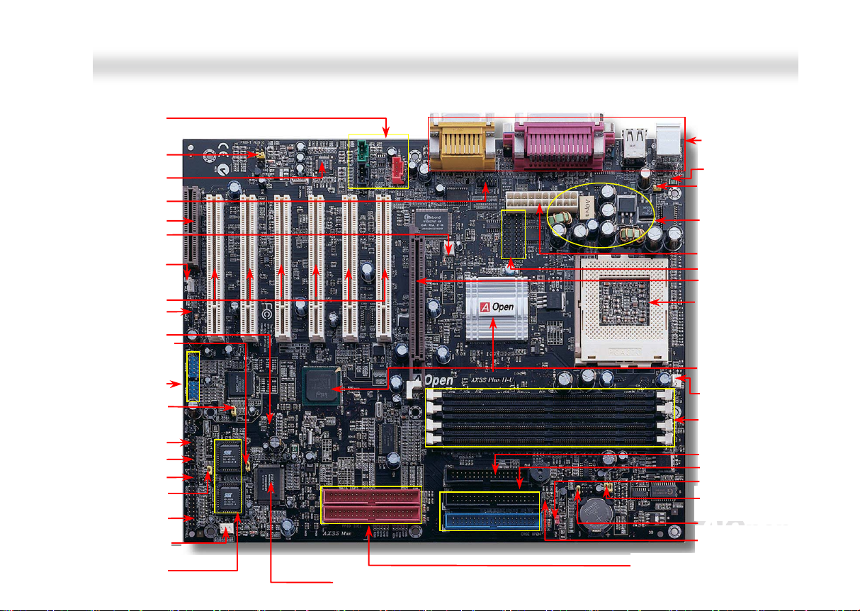
p
A
A
p
A
(
g)
r
r
d
r
(
)
ecto
g
A
(
y)
AAXX33SS MMaaxx//AAXX33SS PPlluuss IIII--UU OOnnlliinnee MMaannuuaall
Red: MODEM-CN
Green: AUX-IN
Black: CD-IN
Front Audio Connector
AC97 CODEC Chipset
COM2 Port Connector
32-bit PCI Expansion Slot x6
(PCI 5 & 6 support slave mode
WOM (Wake On Modem)
2nd USB Port Connector
JP35 IDE RAID Controller
r
3
& 4th USB Port Connector
Enable/Disable Jumpe
CNR Expansion Slot
AUX Fan Connector
w/o H/W Monitorin
WOL (Wake On LAN)
Connecto
PCI cards only)
Connecto
Enable/Disable Jumper
AX3S Max onl
JP34 USB 3&4
Dr. LED Connector
JP30 Die Hard BIOS
Select Jumper
Front Panel Conn
System Fan Connector
Die Hard BIOS with 100%
Virus Protection (Optional)
with H/W Monitorin
Optional
Motherboard Map
PC99 Colored Back
Panel
Resettable Fuse
Keyboard Wake-Up
Select Jum
2200μf Low ESR
Capacitors
TX Power Connector
DVO Connectors
GP 4X Expansion Slot
370-pin CPU Socket with
Frequency/Voltage Auto-detection
that supports Intel
(Both Tualatin & Coppermine
are supported) & Celeron
533MHz~1.2GHz+
Intel® 815E B-Step Chipset
with Pure Aluminum Heatsink
CPU Fan Connector
with H/W Monitoring
PC-100/133 DIMM Slot
x4 supports maximum
to 512MB
u
TA 33/6 6/100 IDE Connector x2
JP14 CMOS Clear Jumper
Dr. Voice Language Select
Jumper
r
18
Promise® FastTrak 100™ Lite IDE RAID Controller
(AX3S Max only)
TA/100 IDE RAID Connector x2
(AX3S Max only)
JP23 FSB Select Jumper
Chassis Intrusion
Connector
er
®
Pentium III
Page 19
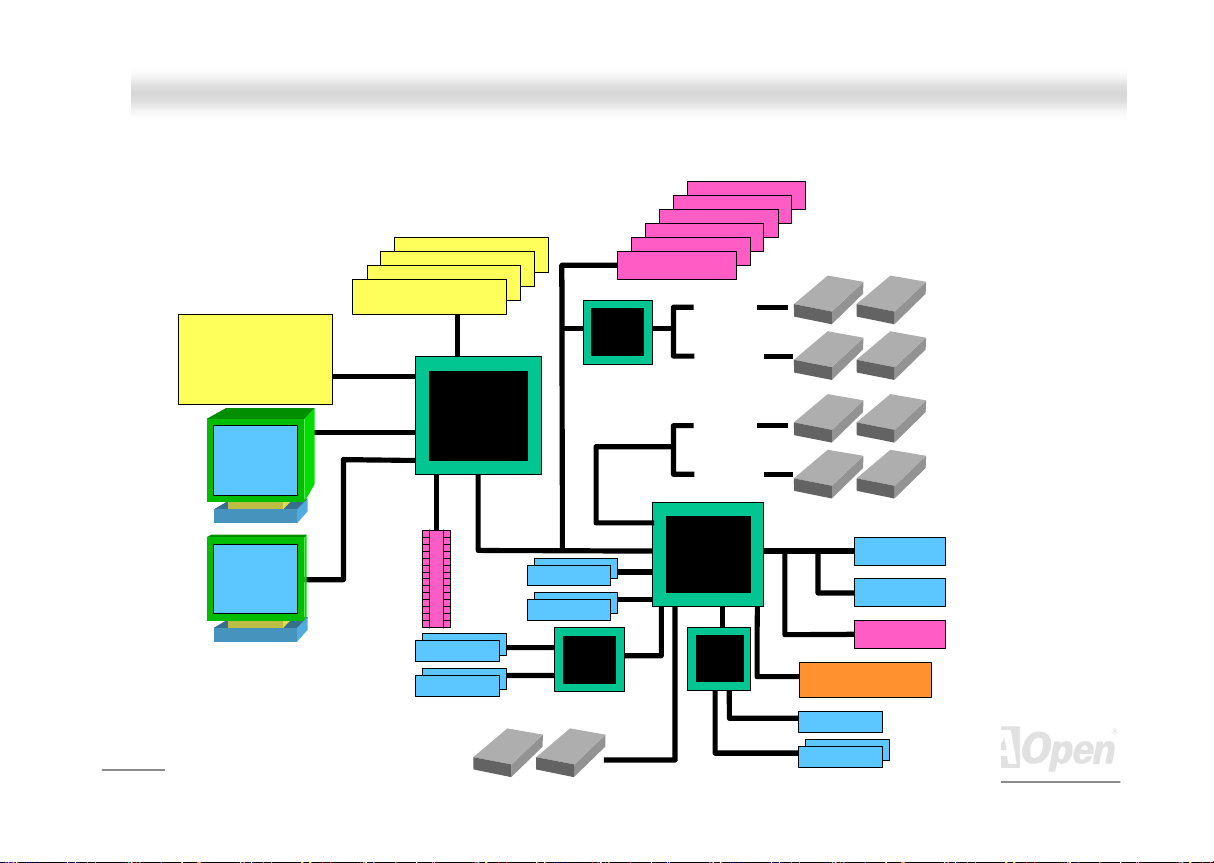
AAXX33SS MMaaxx//AAXX33SS PPlluuss IIII--UU OOnnlliinnee MMaannuuaall
BBlloocckk DDiiaaggrraamm
Socket 370 Intel
Pentium III/Celeron
CPU (Both Tualatin &
Coppermine are supported)
CRT
Monitor
LCD
Monitor
15-pin D-Sub
DVO Connector
USB Connector
DIMM Socket x4
66/100/133MHz
System Bus
Connector
AGP 4X Slot
x4
PC-100/133 SDRAM
Up to 512MB
Intel 815E B-
Step
FW82815
GMCH
USB
Connector
x4
3rdUSB Port
4thUSB Port
PCI Bus
1stUSB Port
2ndUSB Port
USB 2.0
Host
Controller
32-bit PCI Slot x6
Promis e
FastTrak
100 IDE
RAID
Controller
ATA
33/66100
Primary
Channel
Secondary
Channel
Primary
Channel
Secondary
Channel
Intel
FW82801BA
ICH2
Low Pin
Count
Super
I/O
Supports ATA100 IDE RAID 0
and RAID 1 So l ution (AX3S
Max onl y)
AC’97 Link
Firmware Hub
Audio CODEC
Modem CODEC
CNR Slot
4Mbit Flash EEPROM
Parallel Port
IDE Dr i v e x4
IDE Dr i v e x4
Flopp y Disk Drive x2
19
Serial Port x2
Page 20

AAXX33SS MMaaxx//AAXX33SS PPlluuss IIII--UU OOnnlliinnee MMaannuuaall
HHaarrddwwaarree IInnssttaallllaattiioonn
This chapter describes jumpers, connectors and hardware devices of this motherboard.
Note: El ectrostatic discharge (ESD) can damage your processor, disk drives, expansion boards, and
other components. Always observe the following precautions before you install a system component.
1. Do not remove a component from its protective packaging until you are ready to install it.
2. Wear a wrist ground strap and attach it to a metal part of the system unit before handling a
component. If a wrist strap is not available, maintain contact with the system unit t hroughout any
procedure requiring ESD protection.
20
Page 21

AAXX33SS MMaaxx//AAXX33SS PPlluuss IIII--UU OOnnlliinnee MMaannuuaall
AAbboouutt ““OOppttiioonnaall”” aanndd ““UUppggrraaddee OOppttiioonnaall””……
When you read this online manual and start to assemble your computer system, you may find some of functions are called
“Optional”, and some are called “Upgrade Optional”. Though all AOpen motherboards include many amazing and powerful
features, in some situations, these powerful features are not used to every user. Hence, we changed some key features as
“Optional” for you to choose. Some optional functions that can be upgraded by users, we call them “Upgrade Optional”. As for
those optional functions that can’t be upgraded by ourselves, we call them “Optional”. If needed, you can contact our local
distributors or resellers for purchasing “Upgrade Optional” components, and again you can visit AOpen official web site:
www.aopen.com.tw
for more detail information.
21
Page 22
AAXX33SS MMaaxx//AAXX33SS PPlluuss IIII--UU OOnnlliinnee MMaannuuaall
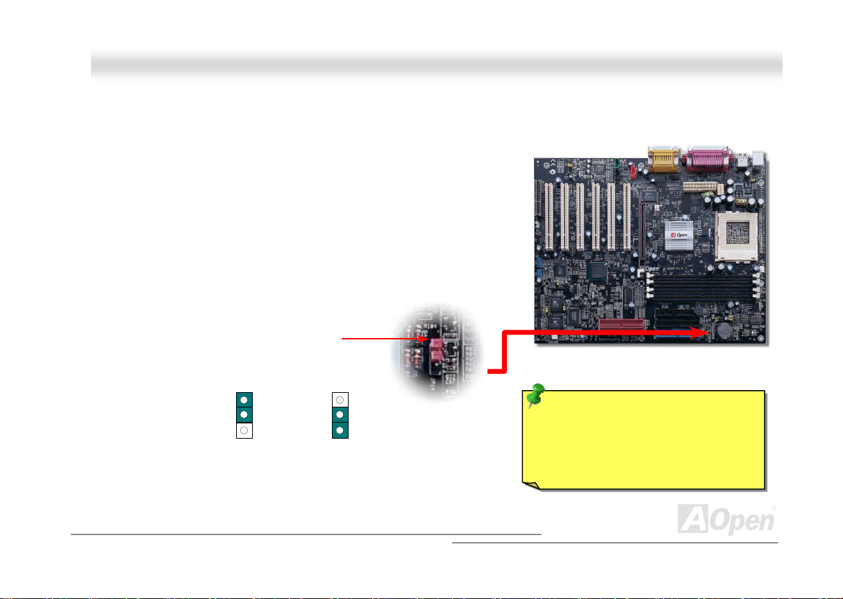
JJPP1144 CClleeaarr CCMMOOSS DDaattaa
You can clear CMOS to restore system default setting. To clear the CMOS, follow the procedure below.
1. Turn off the s ystem and unplug the AC power.
2. Remove ATX power cable from connector PW R2.
3. Locate JP14 and short pins 2-3 for a few seconds.
4. Return JP14 to its normal setting by shorting pins 1 & pin2.
5. Connect ATX power cable back to connector PWR2.
11
Normal Operation
(default)
Pin 1
Clear CMOS
Tip: W hen should I Clear CMOS?
1. Boot fa il bec aus e of ove rc lock i ng…
2. Forget password…
3. Troubleshooting…
22
Page 23
AAXX33SS MMaaxx//AAXX33SS PPlluuss IIII--UU OOnnlliinnee MMaannuuaall
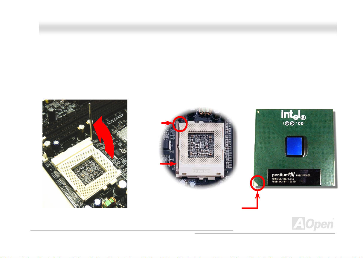
CCPPUU IInnssttaallllaattiioonn
This motherboard supports Intel® Pentium III®(Both Coppermine and Tualatin are supported) and Celeron™ Socket 370 series
CPU. Be careful of CPU orientation when you pl ug it into CPU socket.
1. Pull up the CPU socket level and
up to 90-degree angle.
2. Locate Pin 1 in the socket and look for a black dot or cut edge on t he
CPU upper interface. Match Pin 1 and cut edge, then ins ert the CPU into
the socket.
CPU pin 1
and cut edge
CPU socket
Lever
CPU cut edge
23
Page 24
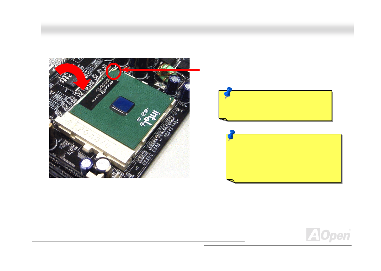
y
/
t
AAXX33SS MMaaxx//AAXX33SS PPlluuss IIII--UU OOnnlliinnee MMaannuuaall
3. Press down the CPU socket level and finish
CPU installation.
CPU cut edge
Note: If you do not match the CPU
socket Pin 1 and CPU cut edge well, it
ma
damage the CPU.
Note: This socket supports FC-PGA
FC-PGA2 package CPU, which is the
latest CPU package developed by Intel.
We strongly recommend you not to inser
former PPGA-package CPU onto it.
24
Page 25
AAXX33SS MMaaxx//AAXX33SS PPlluuss IIII--UU OOnnlliinnee MMaannuuaall
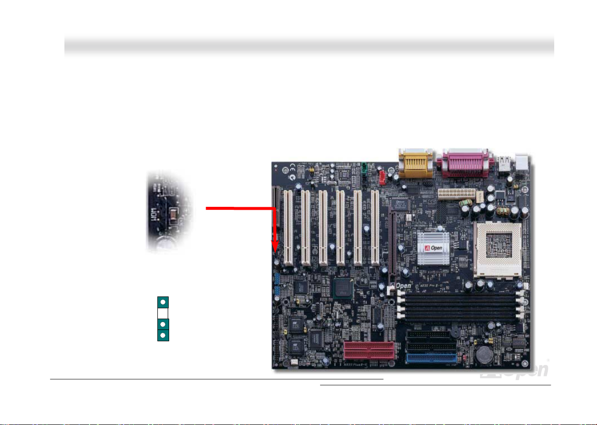
JJPP2233 FFSSBB//PPCCII CClloocckk RRaattiioo
This jumper is used to specify the relationship of PCI and FSB clock. Generally speaking, if you are not overclockers, we
recommend you to set at the default setting. By the way, this motherboard also provides “1MHz S tepping Adjus tment ” feature
for overclockers. You can adjust CPU FSB frequency via BIOS setup program. Based on the CPU type, the adjustment range
has three level: 66~83 (FSB=66MHz, such as Celeron™ 533), 75~124 (FSB=100, such as Pentium
(FSB=133, such as Pentium
Adjustment” range will be changed and following JP23 setting.
®
III 800EB) MHz for your choosing. If you fix the CPU FSB frequency by JP23, the “1MHz St epping
®
III 800E), 100~248
Auto
8
7
FSB=133
FSB=100
FSB=66
2
1
(Default)
25
Page 26
AAXX33SS MMaaxx//AAXX33SS PPlluuss IIII--UU OOnnlliinnee MMaannuuaall
PCI Clock = CPU FSB Clock / Clock Ratio
AGP Clock = PCI Clock x 2
Clock Ratio CPU (Host ) PCI AGP Memory
2X 66MHz 33MHz 66MHz PCI x3
2X, overclocking 75MHz 37.5MHz 75MHz PCI x3
3X 100MHz 33MHz 66MHz PCI x3
3X, overclocking 112MHz 38.3MHz 76.6MHz PCI x3
4X 133MHz 33MHz 66MHz PCI x3 or x4
4X, overclocking 155MHz 37. 5MHz 75MHz PC I x3 or x4
Warning: Intel® 815E B-Step chipset supports
maximum 133MHz FSB and 66MHz A GP clock, higher
clock setting may cause serious system damage.
26
Page 27
AAXX33SS MMaaxx//AAXX33SS PPlluuss IIII--UU OOnnlliinnee MMaannuuaall
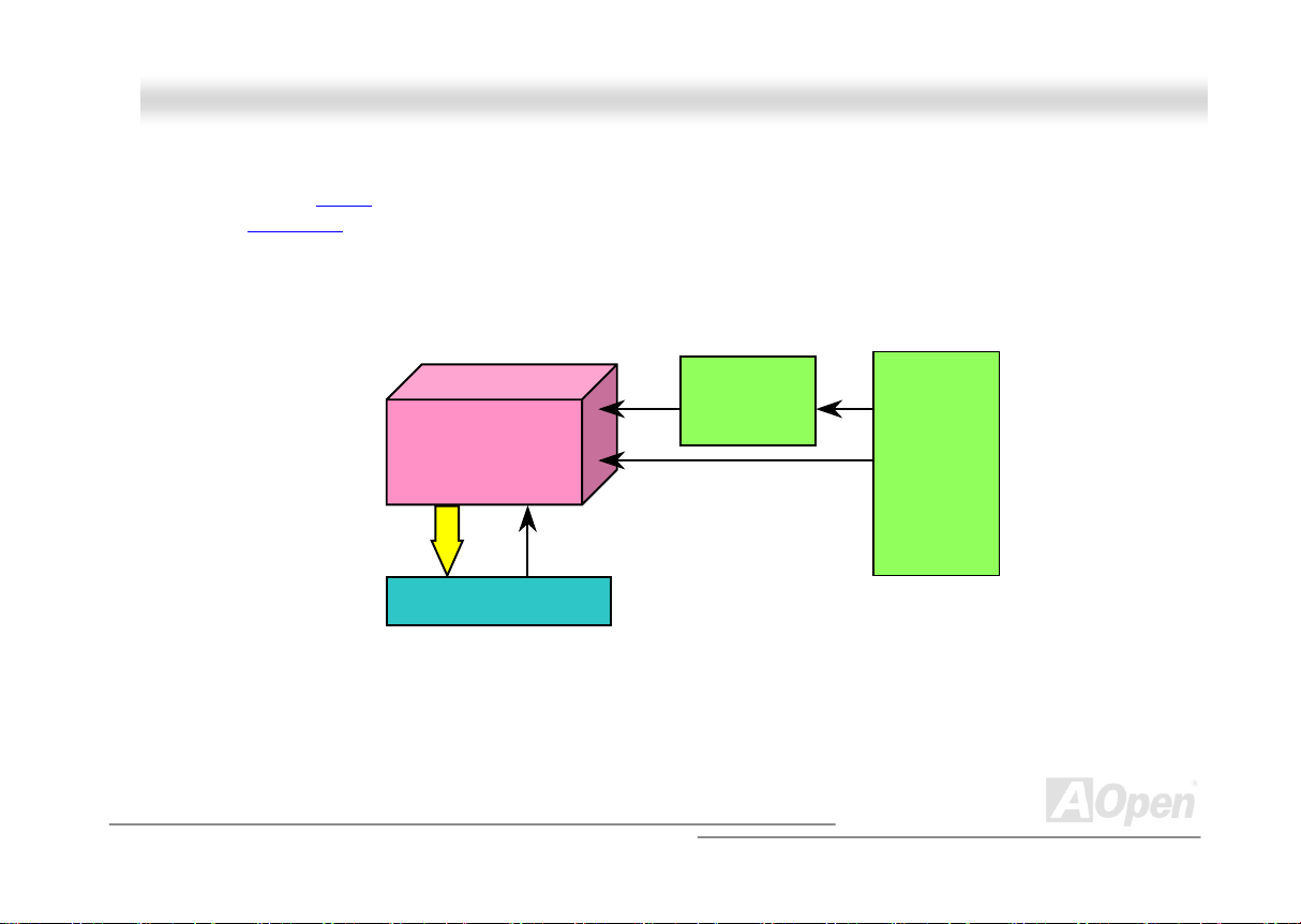
CCPPUU JJuummppeerr--lleessss DDeessiiggnn
CPU VID signal and SMbus clock generator provide CPU voltage auto-detection and allows the user to s et the CPU frequency
through the BIOS setup
designs are eliminated. There will be no worry of wrong CPU voltage detection.
, therefore no jumpers or switches are used. The disadvantages of the Pentium based jumper-less
Intel® Socket 370
Pentium III &
Celeron CPU
CPU VID signal
Power Regulator
(Automatically generates CPU voltage)
CPU Freq. Ratio
CPU voltage
Clock
Generator
BIOS
Controlled
Circuit
27
Page 28
AAXX33SS MMaaxx//AAXX33SS PPlluuss IIII--UU OOnnlliinnee MMaannuuaall
FFuullll--rraannggee AAddjjuussttaabbllee CCPPUU CCoorree VVoollttaaggee
This function is dedicated to overclockers, AOpen works together with Fairchild t o develop a special chip FM3540 that s upports
Adjustable CPU Core Voltage from 1.05V to 1.825 by 0.05 st epping. But this motherboard can also automatically detect CPU
VID signal and generates proper CPU c ore voltage.
BIOS Setup > Frequency/Voltage Control > CPU Voltage Setting
Warning: Higher CPU core voltage may be
able to increase CPU speed for overclocking,
but you may damage the CPU or reduce the
CPU lifecycle
28
Page 29
AAXX33SS MMaaxx//AAXX33SS PPlluuss IIII--UU OOnnlliinnee MMaannuuaall
SSeettttiinngg CCPPUU FFrreeqquueennccy
This motherboard is CPU jumper-less design, you can set CPU frequency through the BIOS setup, and no j umpers or switches
are needed.
y
BIOS Setup > Frequency/Voltage Control > CPU Speed Setting
CPU Ratio
CPU FSB
(By BIOS Table)
CPU FS B
(1 MHz Stepping
by manual
Adjustm e nt )
3x, 3.5x, 4x, 4.5x, 5x, 5.5x, 6x, 6.5x, 7x, 7.5x, 8 x, 8.5x, 9x, 9.5 x, 10x, 10.5 x, 11x,
11.5x, and 12x
66.6, 66.8, 68.3, 70, 75, 80, 83, 100, 100.2, 103, 105 , 110, 115, 120, 124, 133.3,
133.6, 137, 140, 145, 150, 160 , 166. 5 and 200 MH z
FSB = 66, 66~83MHz
FSB = 100, 75~124MHz
FSB = 133, 100~248MHz
Warning: Intel® 815E B-Step chipset supports
maximum 133MHz FSB and 66MHz AGP clock,
higher clock setting may cause serious system
damage.
Tip: If your syst em hangs or fails to boot because
of overclocking, simply use <Home> key to
Home
restore the default setting (433MHz) or you can
wait the AOpen “Watch Dog Timer” reset the
system after five seconds and system will
auto-detect hardware again.
29
Page 30
y
AAXX33SS MMaaxx//AAXX33SS PPlluuss IIII--UU OOnnlliinnee MMaannuuaall
SSuuppppoorrtteedd CCPPUU FFrreeqquueennccyy
Core Frequency = CPU Bus Clock * CP U Ra tio
PCI Clock = CPU Bus Clock / Clock Ratio
AGP Clock = PCI Clock x 2
CPU
Celeron 533 533MHz 66MHz 8x
Celeron 566 566MHz 66MHz 8.5x
Celeron 600 600MHz 66MHz 9x
Celeron 667 667MHz 66MHz 10x
Celeron 700 700MHz 66MHz 10.5
Celeron 766 766MHz 66MHz 11.5x
Celeron 800 800MHz 100MHz 8x
Celeron 850 850MHz 100MHz 8.5x
Celeron 900 900MHz 100MHz 9x
Celeron 1.2G 1.2GHz 100MHz 12x
Pentium III 500E 500MHz 100MHz 5x
Pentium III 600E 600MHz 100MHz 6x
Pentium III 650E 650MHz 100MHz 6.5x
Pentium III 700E 700MHz 100MHz 7x
CPU Core
Frequenc y
Note: This motherboard support CPU
auto-detection function. Hence, you
don’t need to setup the CPU frequency
manuall
.
FSB Clock Ratio
30
Page 31

AAXX33SS MMaaxx//AAXX33SS PPlluuss IIII--UU OOnnlliinnee MMaannuuaall
Pentium III 750E 750MHz 100MHz 7.5
Pentium III 800E 800MHz 100MHz 8x
Pentium III 850E 850MHz 100MHz 8.5x
Pentium III 533EB 533MHz 133MHz 4x
Pentium III 600EB 600MHz 133MHz 4.5x
Pentium III 667EB 667MHz 133MHz 5x
Pentium III 733EB 733MHz 133MHz 5.5
Pentium III 800EB 800MHz 133MHz 6x
Pentium III 866EB 866MHz 133MHz 6.5
Pentium III 933EB 933MHz 133MHz 7x
Pentium III 1G 1GHz 133MHz 7.5x
Pentium III 1.13G 1.13GHz 133MHz 8.5x
Warning: Intel® 815E B-Step chipset supports maximum 133MHz
Bus and 66MHz AGP clock, higher clock setting may cause serious
system damage.
Warning: To avoid possible CPU damage caused by overheating, an automatic
shutdown of system had been espec ially designed on this motherboard. System
would be automatically power off when this motherboard with implementation of
THERMTRIP circuit detected a CPU temperature above 135 degree for 4
seconds.
31
Page 32

AAXX33SS MMaaxx//AAXX33SS PPlluuss IIII--UU OOnnlliinnee MMaannuuaall
AAOOppeenn ““WWaattcchh DDoogg TTiimmeerr””
With this motherboard, AOpen provides a very special, useful feature for overclockers. When you power-on the system, the
BIOS will check last system POST
the CPU FSB
reset the system to reboot in five seconds. Then, BIOS will detect the CPU’s default frequency and POST again. With this
special feature, you can easily overclock your system to get higher system performance, and without removing the cover of
system housing to set the jumper to clear CMOS data when your s ystem hanged.
frequency by user’s setting that stored in the BIOS. If system failed in BIOS POST, the “Watch Dog Timer” will
AOpen
Watch Dog
Timer
status. If it succeeded, the BIOS will enable “Watch Dog Timer” function immediately, and set
Enable/Disable Signal
from BIOS
Countdown about
5 seconds if fails
in POST
Reset Signal
Clock Generator
32
BIOS
CPU ID Signal
CPU
Page 33

AAXX33SS MMaaxx//AAXX33SS PPlluuss IIII--UU OOnnlliinnee MMaannuuaall
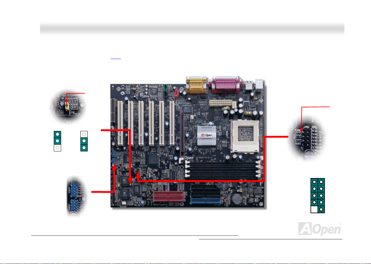
CCPPUU aanndd HHoouussiinngg FFaann CCoonnnneeccttoorr ((wwiitthh HH//WW MMoonniittoorriinngg))
Plug in the CPU fan cable to the 3-pin CPU FAN connector. If you have chassis fan, you can also plug it on S ystem Fan or AUX
FAN (without H/W monitoring) connector.
FAN2 Connector
GND
+12V
SENSOR
FAN3 Connector
GND
+12V
SENSOR
CPU Fan Connector
Note: Some CPU fans do
not have sensor pin, so that
cannot support hardware
monitoring function.
34
Page 34

AAXX33SS MMaaxx//AAXX33SS PPlluuss IIII--UU OOnnlliinnee MMaannuuaall
DDIIMMMM SSoocckkeettss
This motherboard has four 168-pin DIMM sockets that allow you to install PC100 or PC133 memory up to 512MB. The AX3S
Max/AX3S Plus II-U motherboard supports Non-ECC/ECC
and Registered SDRAM.
DIMM1
DIMM2
DIMM3
DIMM4
35
Page 35

AAXX33SS MMaaxx//AAXX33SS PPlluuss IIII--UU OOnnlliinnee MMaannuuaall
DIMM can be single side or double s ide; it has 64 bit data and 2 or 4 clock signals. We st rongly recommend choosing 4-clock
SDRAM for its reliabil ity
Note: Based on Intel 815E B-Step chipset specification, we
recommend you that using double-side SDRAM modules with DIMM
socket 1 & 2. By the way, do not insert the single-side DIMM module
in the DIMM socket 4 when DIMM socket 3 left blank. This will cause
the size report error of DIMM.
SDRAM DIMM Modul e
ECC-Register DIMM Modul e
36
Page 36

AAXX33SS MMaaxx//AAXX33SS PPlluuss IIII--UU OOnnlliinnee MMaannuuaall
HHooww ttoo IInnssttaallll MMeemmoorryy MMoodduulleess
Please follow the procedure as shown below t o finish memory installation.
1. Make sure the DIMM module’s pin face down and match the socket’s size as depicted below.
2. Insert the module straight down to the DIMM slot with bot h hands and press down firmly until the DIMM module is securely
in place.
3. Repeat step 2 to finish additional DIMM modules installation.
Tab
20 pins 60 pins 88 pins
Note: The ta bs of t he DIMM slot
will close-up to hold the DIMM in
place when the DIMM touches
the slot’s bottom.
37
Page 37

p
AAXX33SS MMaaxx//AAXX33SS PPlluuss IIII--UU OOnnlliinnee MMaannuuaall
SSttaannddbbyy PPoowweerr aanndd BBoooott IInnddiiccaattee LLEEDD
Standby Power LED is used to indicate that the standby power is ready to use when it is lighting. And flickering Boot LED means
that the POST is in the process, and it will keep on lighting even aft er POST is done. They are both very useful indicators, which
is used to examine the status of your system.
Boot LED
Standby
ower LED
Warning: Do not install or remove the
DIMM module when the RAM power LED
is lighting.
38
Page 38

e
V
V
V
A
AAXX33SS MMaaxx//AAXX33SS PPlluuss IIII--UU OOnnlliinnee MMaannuuaall
FFrroonntt PPaanneell CCoonnnneeccttoorr
Attach the power LED, speaker, power and reset switch connectors to th
corresponding pins. If you enable “Suspend Mode” item in BIOS Setup, the ACPI
& Power LED will keep flashing while the s ystem is in suspend mode.
Locate the power switch cable from your ATX housing. It is 2-pin female
connector from the housing front panel. Plug this connector to the soft-power
switch connector marked SPWR.
Suspend Type ACPI L E D
Power on Suspend (S1) Flashing for every second
Suspend to RAM (S3) or Suspend to Disk (S4) The LED will be turned off
IDE LED
Speaker
1
SPWR
IDE LED
CPI & PWR
LED
Reset
IDE LED
SPEAKER
NC
NC
+5
+5
+5
GND
NC
1
SPWR
GND
ACPILED-
GND
ACPILED
NC
NC
GND
RESET
GND
39
Page 39

AAXX33SS MMaaxx//AAXX33SS PPlluuss IIII--UU OOnnlliinnee MMaannuuaall
AATTXX PPoowweerr CCoonnnneeccttoorr
The ATX power supply uses 20-pin connector shown below. Make sure you plug in the right direction.
COM
+5V
COM
+3.3V
+3.3V
+3.3V
-12V
COM
PS-ON
COM
+5V
COM
PW-OK
5VSB
+12V
+5V
+5V
-5V
COM
COM
40
Page 40

AAXX33SS MMaaxx//AAXX33SS PPlluuss IIII--UU OOnnlliinnee MMaannuuaall
AACC PPoowweerr AAuuttoo RReeccoovveerryy
A traditional ATX system should remain at power off stage when AC power resumes from power failure. This design is
inconvenient for a network server or works tation, without an UPS, that needs to keep power-on. This motherboard implements
an AC Power Auto Recovery f unction to solve t his problem.
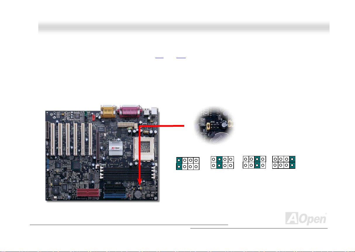
KKeeyybbooaarrdd//MMoouussee WWaakkee--uupp
This motherboard provides keyboard/mouse wake-up function. You can use the JP28 to enable or dis able this function.
JP28
KB/Mouse Wake-up
Pin 1
Disable
(Default)
Enable
41
Page 41

(
(
r
(
A
AAXX33SS MMaaxx//AAXX33SS PPlluuss IIII--UU OOnnlliinnee MMaannuuaall
IIDDEE,, FFllooppppyy,, IIDDEE RRAAIIDD ((AAXX33SS MMaaxx OOnnllyy)) CCoonnnneeccttoorr
Connect 34-pin floppy cable and 40-pin, 80-wire IDE cable to floppy connector FDC and IDE / IDE RAID connector. Be careful of
the pin1 orientation. Wrong orientation may cause system damage.
RAID IDE 2
Slave (4th)
RAID IDE 1
2nd)
Slave
RAID IDE 2
Master
3rd)
RAID IDE 1
Maste
1st)
42
Pin 1
Primary
Slave (2nd)
Pin 1
Secondary
Slave (4th)
Secondary
Master (3rd)
IDE2 (Secondary)
IDE1 (Primary)
TA 33/66/100
IDE Connector
Primary
Master (1st)
FDD
Connector
Page 42

AAXX33SS MMaaxx//AAXX33SS PPlluuss IIII--UU OOnnlliinnee MMaannuuaall
IDE1 is also known as the primary channel and IDE2 as the secondary channel. Each channel supports two IDE devices that
make a total of four devices. In order to work together, the two devices on each channel must be set differently to Master and
Slave mode. Either one can be the hard disk or the CDROM. The setting as master or slave mode depends on the jumper on
your IDE device, so please refer to your hard disk and CDROM manual accordingly.
This motherboard supports ATA33
modes. The IDE bus is 16-bit, which m eans every transfer is two bytes.
Mode Clock Period Clock
PIO mode 0 30ns 20 600ns (1/600ns) x 2byte = 3.3MB/s
PIO mode 1 30ns 13 383ns (1/383ns) x 2byte = 5.2MB/s
PIO mode 2 30ns 8 240ns (1/240ns) x 2byte = 8.3MB/s
PIO mode 3 30ns 6 180ns (1/180ns) x 2byte = 11.1MB/s
PIO mode 4 30ns 4 120ns (1/120ns) x 2byte = 16.6MB/s
DMA mode 0 30ns 16 480ns (1/480ns) x 2byte = 4. 16MB/s
DMA mode 1 30ns 5 150ns (1/150ns) x 2byte = 13.3MB/s
DMA mode 2 30ns 4 120ns (1/120ns) x 2byte = 16.6MB/s
UDMA 33 30ns 4 120ns (1/120ns) x 2byte x2 = 33MB/s
UDMA 66 30ns 2 60ns (1/60ns) x 2byte x2 = 66MB/s
UDMA100 20ns 2 40ns (1/40ns) x 2byte x2 = 100MB/s
Warning: Th e sp ec ific at io n of the I DE c abl e is a max imu m of 46c m (1 8 inc hes ) ;
make sure your cable does not exceed this length.
, ATA66 or ATA100 IDE devices. Following table lists the transfer rate of IDE PIO and DMA
Count
Cycle Time Data Transfer Rate
Tip:
1. For better signal quality,
it is recommended to set
the far end side device
to master mode and
follow the suggested
sequence to install your
new device. Please refer
to above diagram
2. To achieve the best
performance of Ultra
DMA 66/100 hard disks,
a special 80-wires IDE
cable for Ultra DMA
1 i r
ir
.
43
Page 43

AAXX33SS MMaaxx//AAXX33SS PPlluuss IIII--UU OOnnlliinnee MMaannuuaall
JJPP3355 EEnnaabbllee//DDiissaabbllee OOnnbbooaarrdd IIDDEE RRAAIIDD CCoonnttrroolllleerr ((AAXX33SS MMaaxx OOnnllyy))
The JP35 is used to enable or disable onboard PROMISE® FastTrak 100 Lite IDE RAID controller. If you want to disable this
controller, please turn off the system power first, and short pin 2 and pin 3 of JP35 by jumper.
11
Enable
(Default)
Pin 1
Disable
44
Page 44

X
AAXX33SS MMaaxx//AAXX33SS PPlluuss IIII--UU OOnnlliinnee MMaannuuaall
IIrrDDAA CCoonnnneeccttoorr
The IrDA connector can be configured to support wireless infrared m odule, with this module and application software such as
Laplink or Windows 95 Direct Cable Connection, the us er can transfer files to or from laptops, notebooks, PDA devic es and
printers. This connector supports HPSIR (115.2Kbps, 2 meters) and ASK-IR (56Kbps).
Install the infrared module onto the IrDA connector and enable the infrared function f rom BIOS Setup, UART Mode, make sure
to have the correct orientation when you plug in the IrDA connector.
IR_T
IrDA Connector
NC
+5V
Pin 1
GND
IR_RX
45
Page 45
AAXX33SS MMaaxx//AAXX33SS PPlluuss IIII--UU OOnnlliinnee MMaannuuaall
WWOOMM ((ZZeerroo VVoollttaaggee WWaakkee oonn MMooddeemm)) CCoonnnneeccttoorr
This motherboard implements special circuit to support Wake On Modem, both Internal modem card and external box modem
are supported. Since Internal modem card consumes no power when system power is off, it is recommended to use an internal
modem. To use internal modem, connect 4-pin cable from RING connector of modem card to the WOM connector on the
motherboard.
WOM Connector
+5VSB
NC
RI-
GND
46
Page 46

AAXX33SS MMaaxx//AAXX33SS PPlluuss IIII--UU OOnnlliinnee MMaannuuaall
WWOOMM bbyy EExxtteerrnnaall BBOOXX MMooddeem
Traditional Green PC suspend mode does not really turn off the system power supply, it uses external box modem to trigger MB
COM port and resume back to active.
m
Serial Port
(Modem Side)
Pin 1
(Motherboard Side)
Serial Port
47
Page 47

AAXX33SS MMaaxx//AAXX33SS PPlluuss IIII--UU OOnnlliinnee MMaannuuaall
WWOOMM bbyy IInntteerrnnaall MMooddeemm CCaarrd
With the help of the ATX soft power On/Off, it is possible to have a system totally power off, and wakeup to automatically answer
a phone call as an answering machine or to send/receive a fax. You may identify whether or not your system is in true power off
mode by checking to see if the fan of your power supply is off. Both an external box modem and an internal m odem card can be
used to support Modem Wake Up, but if you use an external modem, you have to leave your box modem on.
WOM Connector
(Motherboard Side)
d
WOM Connector
(Modem Card Side)
48
Page 48

AAXX33SS MMaaxx//AAXX33SS PPlluuss IIII--UU OOnnlliinnee MMaannuuaall
WWOOLL ((WWaakkee oonn LLAANN))
This feature is very similar as Wake On Modem, but it goes through local area network. To use Wake On LAN function, you must
have a network card with chipset that supports this feature, and connect a cable from LAN card to motherboard WOL c onnector.
The system identification information (probably IP address) is stored on network card and because there is a lot of traffic on the
Ethernet, you need to install network management software, such as ADM, for the checking of how to wake up t he system. Note
that, at least 600mA ATX standby current is required to support the LAN card for this function.
LID
GND
+5VSB
49
Page 49

AAXX33SS MMaaxx//AAXX33SS PPlluuss IIII--UU OOnnlliinnee MMaannuuaall
WOL Connector
(Motherboard Side)
WOL Connector
(Ethernet Card Side)
50
Page 50

AAXX33SS MMaaxx//AAXX33SS PPlluuss IIII--UU OOnnlliinnee MMaannuuaall
AAGGPP ((AAcccceelleerraatteedd GGrraapphhiicc PPoorrtt)) EExxppaannssiioonn SSlloott
The AX3S Max/AX3S Plus II-U provides an AGP 4x slot. The AGP 4x is a bus interface targeted for high-performance 3D
graphic. AGP supports only memory read/write operation and single-master single-slave one-to-one only. A GP uses both rising
and falling edge of the 66MHz clock, for 2X AGP, the data transfer rate is 66MHz x 4bytes x 2 = 528MB/s. AGP is now moving
to AGP 4x mode, 66MHz x 4bytes x 4 = 1056MB/s.
51
Page 51

AAXX33SS MMaaxx//AAXX33SS PPlluuss IIII--UU OOnnlliinnee MMaannuuaall
DDVVOO CCoonnnneeccttoorr
The AX3S Max/AX3S Plus II-U provides a DVO (Digital Video Output) connector which transferring the VGA s ignal to the AOpen
Digital Video/TV Riser Card. W ith this connector and riser card, you can connect the digital LCD panel with computer to get high
quality picture.
DVO 1 & 2
Connector
AOpen Digital
Video/TV Riser Card
5V
NC
NC
GND
FTVSYNC
FTHSYNC
GND
3VFTSCL
VFT
DA
DVO CN 2
1 2
5V
SL_STALL
3.3V
GND
PCIRST1GND
3.3V
GND
FTBLNK-
1.8V
11 20
52
FTD1
GND
FTD3
FTD5
FTD6
FTCLK0
3.3V
FTD9
FTD11
DVO CN 1
1 2
FTD0
FTD2
3.3V
FTD4
GND
FTCLK1
FTD7
FTD8
FTD10
3.3V
11 20
Page 52

AAXX33SS MMaaxx//AAXX33SS PPlluuss IIII--UU OOnnlliinnee MMaannuuaall
CCNNRR ((CCoommmmuunniiccaattiioonn aanndd NNeettwwoorrkk RRiisseerr)) EExxppaannssiioonn SSlloott
CNR is a riser card specification to replace the AMR (Audio/Modem Riser) that supports V.90 analog modem, multi-channel
audio, and phone-line based networking. Owing to CPU computing power getting stronger, the digital processing job can be
implemented in main chipset and share CPU power. The analogy conversion (CODEC
circuit design, which is put on CNR card. This motherboard implements sound CODE C on board (can be disabled by JP12), but
reserve CN R slot fo r t he opt i on of mod em f unc ti on. Not e t hat you c an sti ll use P CI m odem ca rd.
) circuit requires a different and separate
53
Page 53

AAXX33SS MMaaxx//AAXX33SS PPlluuss IIII--UU OOnnlliinnee MMaannuuaall
PPCC9999 CCoolloorr CCooddeedd BBaacckk PPaanneell
The onboard I/O devices are PS/2 Keyboard, PS/2 Mouse, COM1 and 15-pi n VGA Connect or, Printer, eight USB, AC97 sound
and game ports. The view angle of drawing shown here is from the back panel of the housing.
PS/2 Mouse
Connector
USB
Connectors
SPP/EPP/ECP
Parallel Port
MIDI/Game Port
PS/2 Keyboard
PS/2 Keyboard: For standard keyboard, which is us ing a PS/2 plug.
PS/2 Mo us e: For PC- Mou se, wh ic h is us i ng a PS /2 p lu g.
USB Por t : Available for connecting USB devices.
Parallel Port: To connect with SPP/ECP/EPP pri nter.
COM1 Port: To connect with pointing devices, modem or others serial devices.
VGA Connector: To connect with PC m onitor.
Speaker Out: To External Speaker, Earphone or Amplifier.
Line-In: Comes from the signal sources, such as CD/Tape player.
MIC-In: From Microphone.
MIDI/Game Port: For 15-pin PC joystick, game pad or MIDI devices.
Connector
COM 1 Port 15-pin VG A Connector
MIC-In
Line-In
Speaker Out
54
Page 54
AAXX33SS MMaaxx//AAXX33SS PPlluuss IIII--UU OOnnlliinnee MMaannuuaall
SSuuppppoorrtt 88 UUSSBB CCoonnnneeccttoorrss
This motherboard provides 8 USB connectors to connect USB devices, such as mouse, keyboard, modem, printer, etc. There
are two connectors on the PC99 back panel. You can use proper cable to connect other USB connectors to the back panel or
front panel of chassis. By the way, you can us e JP34 to disable USB3 and USB4 if you do not need them.
1
Enable
(Default)
USB3 & 4
Pin 1
Disable
1 2
+5V
SBD3SBD3+
GND
NC
USB2 Connector
+5V
SBD2-
SBD2+
GND
KEY
Pin 1
55
Page 55

AAXX33SS MMaaxx//AAXX33SS PPlluuss IIII--UU OOnnlliinnee MMaannuuaall
CChhaassssiiss IInnttrruussiioonn SSeennssoorr
The “CASE OPEN” header provides chassis intrusion-monitoring function. This function logged the event in the system BIOS
when chassis is opened. You can use the 2-pin chassis intrusion sensor to connect with this header, and enable the chassis
monitoring function of system BIOS.
Sense
GND
Chassis I nt rus i on
Connector
56
Page 56

AAXX33SS MMaaxx//AAXX33SS PPlluuss IIII--UU OOnnlliinnee MMaannuuaall
CCOOMM22 CCoonnnneeccttoorr
The AX3S Max/AX3S Plus II-U provides two s erial port connectors. But, the COM2 port connector of PC99 colored back panel
has been replaced to VGA connector. The COM2 port connector will be mounted on the upper area of M/B. With proper cable,
you can connect it to the back panel of chassis.
Pin 1
DTR#
SIN
COM2 Connector
DSR#
CTS#
2
1
DCD#
SOUT
GND
RTS#
RI#
57
Page 57

AAXX33SS MMaaxx//AAXX33SS PPlluuss IIII--UU OOnnlliinnee MMaannuuaall
CCDD AAuuddiioo CCoonnnneeccttoorr
This connector is used to connect CD Audio cable from CDROM or DVD drive to onboard sound.
R
GND
GND
L
CD-IN
58
Page 58
AAXX33SS MMaaxx//AAXX33SS PPlluuss IIII--UU OOnnlliinnee MMaannuuaall
MMooddeemm AAuuddiioo CCoonnnneeccttoorr
This connector is used to connect Mono In/MIC Out cable from internal modem card to onboard sound circuit. The pin 1-2 is
Mono In, and the pin 3-4 is MIC Out. Please note that there is no standard for this kind of connector yet, only some internal
modem cards implement this connector.
MIC Out
GND
GND
Mono In
MODEM-CN
59
Page 59

AAXX33SS MMaaxx//AAXX33SS PPlluuss IIII--UU OOnnlliinnee MMaannuuaall
AAUUXX--IINN CCoonnnneeccttoorr
This connector is used to connect MPEG Audio cable from MPEG card to onboard sound.
R
GND
GND
L
AUX-IN
60
Page 60

y
AAXX33SS MMaaxx//AAXX33SS PPlluuss IIII--UU OOnnlliinnee MMaannuuaall
FFrroonntt AAuuddiioo CCoonnnneeccttoorr
If the housing has been designed with an audi o port on the front panel, you’ll be able to connect onboard audio to front panel
through this connector. By the way, please remove the jumper cap from the Front Audio Connector before you connect the cable.
Do not remove this yellow jumper cap if hous ing without an audio port on the front panel.
Front Audio Connector
1 2
FP_MIC
NC
PHONE_R
NC
PHONE_L
9 10
GND
+5V
JS1
KEY
NC
Note: Please remove the jumper cap from the Front Panel Audio Connector before
audio port on the front panel.
ou connect the cable. Do not remove this y ellow jumper cap if housing without an
61
Page 61

AAXX33SS MMaaxx//AAXX33SS PPlluuss IIII--UU OOnnlliinnee MMaannuuaall
DDiiee--HHaarrdd BBIIOOSS ((OOppttiioonnaall))
Recently, many viruses have been found that they may destroy bios code and data area. Therefore, this motherboard
implements a very effective hardware prot ection method that does not involve any software or BIOS coding, hence it is 100%
virus free. You may restore the originally mounted BIOS with 2
This motherboard comes with one BIOS ROM, you may contact our local distributor or reseller for purchasing the extra BIOS
ROM. Please visit our website: www.aopen.com
BIOS
ROM
JP30
Pin 1
for details.
nd
BIOS ROM by setting JP30 to pin 2-3 if it fails to act normally.
Rescue
ROM
1
Normal
1
Rescue
62
Page 62

AAXX33SS MMaaxx//AAXX33SS PPlluuss IIII--UU OOnnlliinnee MMaannuuaall
EExxtteerrnnaall CCoonnttrroolllleerr ffoorr DDIIEE--HHAARRDD BBIIOOSS ((OOppttiioonnaall))
External Controller provides you a better and convenience way to switch the BIOS status between “Rescue” and “Normal”
without opening the case of your computer. You have to plug the jumper cable to the c onnector pin (JP 3 0 ) on the motherboard.
Be careful of the orientation when you connect, the red wire should correspond to Pin1.
Manual Switch
To / Form CPU
Read/Write
Normal
Flash ROM
Read Only
Rescue ROM
63
Page 63
p
AAXX33SS MMaaxx//AAXX33SS PPlluuss IIII--UU OOnnlliinnee MMaannuuaall
Note: If you suspect your BIOS is infected by virus, just rescue your bios by following steps:
1. Turn off the system, set the External Controller to “Rescue” to read from rescue ROM.
2. Boot the system and set the switch back to “Normal”.
3. Follow the BIOS upgrade procedure to rehabilitate BIOS.
4. Reboot the system, and you should be able to back to norm al.
Normal
(Read from normal
Flash ROM)
Tip: If y ou place the sw itch to th e middle
rd
(as 3
picture shown), you will not be
able to boot your system, thus you can
rotect your data from molesting.
Rescue
(Read from
Rescue ROM)
Lock
(Lock your computer
to protect your data)
64
Page 64

AAXX33SS MMaaxx//AAXX33SS PPlluuss IIII--UU OOnnlliinnee MMaannuuaall
GGPPOO ((GGeenneerraall PPuurrppoossee OOuuttppuutt)) CCoonnnneeccttoorr
GPO (General Purpose Output) is an advanced specification developed by AOpen for power users to define the further
function by oneself. For example, you c an design a daughter board to provide additional capabilities , such as an alarm, a buzzer,
a timekeeper, etc.
Pin 1
GPO19
GPO20
3.3V
1 6
NC
GND
3 4
65
Page 65

AAXX33SS MMaaxx//AAXX33SS PPlluuss IIII--UU OOnnlliinnee MMaannuuaall
DDrr.. LLEEDD CCoonnnneeccttoorr
In conjunction with Dr. LED (Upgrade Optional), which can easily show what kind of problem may occur on your system during
assembly. It can clearly indicate whether there is a component issue or an installation issue by t he 8 LEDs on the front panel of
Dr. LED. This helps you quickly self-diagnostic your system status.
Pin 1
3.3V
NC
GND
1 2
GPO12
GPO14
GPO14-
5 6
66
Page 66

AAXX33SS MMaaxx//AAXX33SS PPlluuss IIII--UU OOnnlliinnee MMaannuuaall
Dr. LED is a CD disc storage box with 8 LEDs on its front panel, the size of Dr. LED is exactly the same as 5.25 in floppy drive,
so that it can be mount into normal 5.25 in drive bay of any housing.
The total 8 LEDs light up alternatively if the system fails in one of eight stages. Once the LED7 (latest LED) is lit, this indicates
that the system has completed its boot-up procedure.
The 8 LEDs indicate the following messages when lit:
LED 0 - Indicates that the CPU may have been ins talled incorrectly or is damaged.
LED 1 - Indicates that the memory may have been installed incorrectly or is damaged.
LED 2 - Indicates that the AGP may have been installed incorrectly or is damaged.
LED 3 - Indicates that the PCI card may have been installed incorrectly or is damaged.
LED 4 - Indicates that the floppy disk drive may have been i nstalled incorrectly or is damaged.
LED 5 - Indicates that the HDD may have been i nstalled incorrectly or is damaged.
LED 6 - Indicates that the keyboard may have been installed incorrectly or is damaged.
LED 7 - Indi ca tes th at t he sy st em is OK.
7 6 5 4 3 2 1 0
Boot O.K. KB HDD Audio CPU Video MemoryPCI
Note: During POST (Power On Sel f Test) procedure, the
Debug LED will light on sequentially from LED0 to LED7 until
the system boot O.K
67
Page 67

AAXX33SS MMaaxx//AAXX33SS PPlluuss IIII--UU OOnnlliinnee MMaannuuaall
DDrr.. VVooiiccee
The Dr. Voice is a great feature of AX3S Pro-U motherboard, which can identifies what kind of problems had occurred in the
operating system. It can even clearly “tell” whether there is a component issue or an installed issue, such as CPU, memory
module, VGA, PCI add-on card, FDD, HDD or keyboard by voice. The Dr. Voice provides four kinds of language versions,
English, German, Japanese and Chinese for your choosing. You can select preferred language version by JP15 & JP16
jumpers.
JP16
Pin 1
JP16
English
(Default)
Select Jumper
JP15
Dr. Voice
Language
Chinese
JP15
Pin 1
Japanese
German
68
Page 68

A
AAXX33SS MMaaxx//AAXX33SS PPlluuss IIII--UU OOnnlliinnee MMaannuuaall
Auto Switch
RTC
CMOS
Battery ATX Stand-by Power
uto switching to ATX standby
power as long as AC power line is
plugged. This smart design
increases battery life if you still plug
battery on motherboard.
Backup by EEPROM
BBaatttteerryy--lleessss aanndd LLoonngg LLiiffee DDeessiiggnn
This Motherboard implements Flash ROM and a special circuit that allows you to save your current CPU and CMOS Setup
configurations without the need of a battery. The RTC (real time clock) can also keep running as long as the power cord is
plugged. If you lose your CMOS data by accident, you c an just reload the CMOS configurations from Flash ROM and the system
will recover as usual.
Flash
ROM
(Real Time Clock)
00:00:00
69
Page 69
AAXX33SS MMaaxx//AAXX33SS PPlluuss IIII--UU OOnnlliinnee MMaannuuaall
OOvveerr--ccuurrrreenntt PPrrootteeccttiioonn
The Over Current Protection was very popular implemented on ATX 3.3V/5V/12V switching power supply. However, the new
generation CPU uses different voltage that has regulator to transfer 5V to CPU voltage (for example, 2.0V), and makes 5V over
current protection useless. This motherboard is with switching regulator onboard supports CPU over-current protection; in
conjunction with 3.3V/5V/12V power supply provide the full line over-current protection.
Note: Although we have implemented protection circuit try to prevent any human operating
mistake, there is still certain risk that CPU, memory, HDD, add-on cards installed on this
motherboard may be damaged because of component failure, human operating error or unk nown
nature reason. AOpen cannot guaranty the protection circuit will always work perfectly.
ATX
Switching
Power
Supply
12V (Protected by power supply)
3.3V (Protected by power supply)
5V (Protected by power supply)
Onboard
Power
Regulator
Over-Current
Protection
Circuit
CPU Core Voltage
70
Page 70

AAXX33SS MMaaxx//AAXX33SS PPlluuss IIII--UU OOnnlliinnee MMaannuuaall
Fan
CPU
Fan Speed
AOpen H/W
Monitoring
Utility
CPU Temperature
CPU Voltage
System Voltage
Detection
Circuit
HHaarrddwwaarree MMoonniittoorriinngg
This motherboard implements a hardware m onitoring system. As you turn on your system, this smart design will continue to
monitor your system’s working voltage, fan status and CPU temperature. If any of these systems’ status go wrong, there will be
an alarm through the chassis external speaker or buzzer of motherboard (if existed) to warn the user.
Power
71
Page 71

AAXX33SS MMaaxx//AAXX33SS PPlluuss IIII--UU OOnnlliinnee MMaannuuaall
RReesseettttaabbllee FFuussee
Traditional motherboard has fuse for Keyboard and USB port to prevent over-current or shortage. These fuses are soldered
onboard that when it is broken (function as protecting the m otherboard), user still cannot replace it and the motherboard is still
malfunctioning.
With expensive Resettable Fuse, the motherboard can be resumed back to normal function after the fuse had done its
protection job.
Resettable
Fuse
72
Page 72

AAXX33SS MMaaxx//AAXX33SS PPlluuss IIII--UU OOnnlliinnee MMaannuuaall
PPoowweerr BBrriiddggee
All conductors resist the flow of current to some extent and i n order to eliminate resistance to minimum, a most economical way
to reduce resistance is to make conductor as efficient as possible by providing s o-called “conduit” to channel the current flow.
Resistance also creates heat and it has to be reduc ed to a controllable level. What AOpen engineers are doing is to provide a
better path to reach optimum power route to efficiently deliver power (both voltage and current) to destination without creating
heat that’s normally accompanied by high current with resistance during the journey.
In a typical motherboard design, there are 4 layers of copper for the entire circuitry where both VCC and ground are sandwiched
between solder side and component side. In the older generation motherboard when bus speed and component numbers are
low, it is quite sufficient, but as the performance of today’s personal computer has reached to PC133 and operating over 1GHz
in CPU speed, the old method seems to be crippled by dilemma. Today’s motherboard design faces challenge of providing fast
Power Br id ge
73
Page 73

AAXX33SS MMaaxx//AAXX33SS PPlluuss IIII--UU OOnnlliinnee MMaannuuaall
speed with low noise that is detrimental to the system stability. In order to provide every critical part of circuitry within the PCB,
AOpen deploys a new design concept called “Power Bridge”. These bridges are strategically place within the motherboard
design that provides both voltage and current to a targeted PCB region. This extra power is so pure that it contains no inherit
noise when travel through VCC and ground plane. Further, since the extra power is via “Power Bridge”, PCB VCC and Ground
will have lesser current flow through and lesser thermal problem.
Benefits
1. Increase current flow and eliminate accompanied heat
2. Even current distribution within motherboard
3. Better PCB layout and component placement
74
Page 74

AAXX33SS MMaaxx//AAXX33SS PPlluuss IIII--UU OOnnlliinnee MMaannuuaall
0
μμμμ
ffff
2222000
Besides the deployment of Power Bridge, a group of large capacitors that meet the requirements of today’s high performance
motherboard design. The theory behind this is long transmission lines have considerable inductanc e and capacitance as well as
resistance. When a current flows through the line, inductance and capacitance have the effect of varying the voltage on the line
μμμμ
ffff
LLooww EESSRR CCaappaacciittoorr
as the current varies. Thus the supply voltage varies with
the load. Several kinds of devices are used to overcome
this undesirable variation, in an operation called regulation
of the voltage. They include induction regulators and
three-phase synchronous motors (called synchronous
condensers), both of which vary the effective amount of
inductance and capacitance in the transmission circuit.
Inductance and capacitance react with a tendency to
nullify one another. When a load circuit has more inductive
than capacitive reactance, as almost invariably occurs in
large power systems, the amount of power delivered f or a
given voltage and current is less than when the two are
equal. The ratio of these two amounts of power is c alled
the power factor. Because transmission-line losses are
proportional to current, capacitance is added to the circuit
when possible, thus bringing the power factor as nearly as
possible to 1. For this reason, large capacitors are
frequently inserted as a part of power-transmission
systems.
75
Page 75

AAXX33SS MMaaxx//AAXX33SS PPlluuss IIII--UU OOnnlliinnee MMaannuuaall
The power circuit of the CPU core voltage must be checked to ensure system stability for high speed CPUs (such as the new
Pentium III, or when overclocking). A typical CPU core voltage is 2.0V, so a good design should control voltage between 1.860V
and 2.140V. That is, the transient must be below 280mV. B elow is a timing diagram captured by a Digital Storage Scope, it
shows the voltage transient is only 143mv even when maximum 18A current is applied.
Note: This diagram for example only, it m ay not be exactly the same as this motherboard.
76
Page 76

AAXX33SS MMaaxx//AAXX33SS PPlluuss IIII--UU OOnnlliinnee MMaannuuaall
LLaayyoouutt ((FFrreeqquueennccyy IIssoollaattiioonn WWaallll))
Note: This diagram for example only, it may not be exactly
the same as this motherboard.
For high frequency operation, especially overclocking,
layout is the most important factor to make sure
chipset and CPU working in stable condition. The
layout of this motherboard implements AOpen’s
unique design called “ Frequency Isolation Wall”.
Separating each critical portion of motherboard into
regions where each region operates in a same or
similar frequency range to avoid cross talk and
frequency interference between each region’s
operations and condition. The trace length and route
must be calculated carefully. For example, the clock
trace must be equal length (not necessarily as short
as possible) so that clock skew will be controlled
within few a pico second (1/10
12
Sec)
77
Page 77

AAXX33SS MMaaxx//AAXX33SS PPlluuss IIII--UU OOnnlliinnee MMaannuuaall
PPuurree AAlluummiinnuumm HHeeaattssiinnkk
Cool down CPU and Chipset is important for system reliability. Aluminum heat sink provides better heat consumption especially
when you are trying to overclock.
78
Page 78

AAXX33SS MMaaxx//AAXX33SS PPlluuss IIII--UU OOnnlliinnee MMaannuuaall
DDrriivveerr aanndd UUttiilliittyy
There are motherboard drivers and utilities included in AOpen Bonus CD disc. You don’t need to install all of them in order to
boot your system. But after you finish the hardware installation, you have to install your operation system first (such as Windows
98) before you can install any drivers or ut ilities. Please refer to your operation system’s installation guide.
Note: Please follow recommended procedure
to install Windows 95
and Windows 98.
79
Page 79

AAXX33SS MMaaxx//AAXX33SS PPlluuss IIII--UU OOnnlliinnee MMaannuuaall
AAuuttoo--rruunn MMeennuu ffrroomm BBoonnuuss CCDD DDiisscc
You can use the auto-run menu of Bonus CD disc. Choose the utility and driver and select model name.
80
Page 80

AAXX33SS MMaaxx//AAXX33SS PPlluuss IIII--UU OOnnlliinnee MMaannuuaall
EElliimmiinnaattee ““??”” mmaarrkk ffrroomm WWiinnddoowwss 9955//9988
Windows 95/98 cannot recognize this chipset, because it was released before the Intel 815E B-Step chips et. You can install the
Intel INF Update Utility from the Bonus Pack CD disc auto-run m enu to eliminate the “?” marks.
81
Page 81

AAXX33SS MMaaxx//AAXX33SS PPlluuss IIII--UU OOnnlliinnee MMaannuuaall
IInnssttaalllliinngg OOnnbbooaarrdd AAGGPP DDrriivveerr
Intel 815E B-Step chipset i ntegrates a 2D/3D graphics accelerator and provides A GP 2X/4X incredible performance to access
main memory at over 1GB/s. You can find the audio driver from the Bonus Pack CD disc auto-run menu.
Note: If you are using Windows95,
you should install DCOM95 patch
from the Bonus Pack auto-run menu
first, before you install AGP driver.
82
Page 82

AAXX33SS MMaaxx//AAXX33SS PPlluuss IIII--UU OOnnlliinnee MMaannuuaall
IInnssttaalllliinngg UUllttrraa AATTAA//110000 IIDDEE DDrriivveerr
This Intel® Ultra ATA Storage Driver is designed to take advantage of devices supporting ATA DMA/Ultra DMA technologies, and
improve system performance of Windows 98, Windows 98 Second Edition(SE), Windows Millennium Edition(Me), Windows NT*
4.0 (any Service Pack), and Windows 2000 operating systems. However, we could not guarantee it would not trigger any system
instabilities as Intel also suggests it is not a requirement for your operating system to work properly. Nevertheless, if you need
this driver, you c an still find it in the AOpen Bonus Pack
Note: Installing this ATA/100 IDE
driver may cause Suspend to
Hard Drive failure.
CD disc.
83
Page 83

AAXX33SS MMaaxx//AAXX33SS PPlluuss IIII--UU OOnnlliinnee MMaannuuaall
IInnssttaalllliinngg OOnnbbooaarrdd SSoouunndd DDrriivveerr
This motherboard comes with an AD1885 AC97 CODEC. You can find the audio driver from the Bonus Pack CD disc auto-run
menu.
84
Page 84

AAXX33SS MMaaxx//AAXX33SS PPlluuss IIII--UU OOnnlliinnee MMaannuuaall
IInnssttaallll OOnnbbooaarrdd IIDDEE RRAAIIDD DDrriivveerr ((AAXX33SS MMaaxx oonnllyy))
The onboard PROMISE® FastTrak 100 Lite chipset provides DOS, Widows 3.1/95/98/98 SE/ME/NT/2000 driver for install.
Please refer to the “ATA/100 IDE RAID Manual” for get more detail information.
IInnssttaallll FFaassttCChheecckk™™ MMoonniittoorriinngg UUttiilliittyy ((AAXX33SS MMaaxx oonnllyy))
You can monitor the operating status of disk array and drives configured on the IDE RAID channel using the supplies
FastCheck™ monitoring utility for Windows-based operating system. FastCheck™ generates visual and audible messages
alerting you of possible problems with the disk array or controller. Please refer to the “ATA/100 IDE RAID Manual” for get more
detail information.
85
Page 85

AAXX33SS MMaaxx//AAXX33SS PPlluuss IIII--UU OOnnlliinnee MMaannuuaall
AACCPPII SSuussppeenndd ttoo HHaarrdd DDrriivvee
ACPI Suspend to Hard Drive is basically controlled by Windows operation system. It sa ves your current work (system status,
memory and screen image) into hard disk, and then the system can be totally power off. Next time, when power is on, you can
resume your original work directly from hard disk within few seconds without go through the Windows booting process and run
your application again. If your memory is 64MB, normally, you need to reserve at least 64MB HDD space to save your memory
image.
When go into Suspend:
When power-on next time:
System
Image &
Status
System
Image &
Status
Hard
Save into
Restore within
seconds
Disk
Hard
Disk
86
Page 86

AAXX33SS MMaaxx//AAXX33SS PPlluuss IIII--UU OOnnlliinnee MMaannuuaall
System Requirement
1. AOZVHDD.EXE 1.30b or later.
2. Delete config.sys and autoexec.bat.
Fresh installation of Windows 98 on a new system
1. Execute "Setup.exe /p j" to install Windows 98
2. Aft er Windows 98's installation is complete, go to the Control Panel > Power Management.
a. Set Power Schemes > System Standby to "Never".
b. Click on "Hibernate" and select "Enable Hibernate Support" then "Apply".
c. Click on the "Advanced" tab, you'll see "Hibernate" on "Power Buttons". Note that this option will only be s een after step
b mentioned above has been completed; otherwise only "Standby" and "Shutdown" will be shown. Select "Hibernate" and
"Apply".
3. Clean boot into DOS and run AOZVHDD utility.
a. If you ass ign the wh ole disk to your W in 98 system (FAT 1 6 or FAT 32 ), please r un "aozvhdd / c /file". Please remember
sufficient free space has to be reserved in the disk, e.g. if you have 64 MB DRAM and 16 MB VGA card installed, the
system needs at least 80 MB free space. The utility will locate the space automatically.
b. If you assign an individual partition for Win 98, please run "aozvhdd /c /partition". Of course, the system needs to
provid e unf orm at te d an emp ty pa rt iti o n.
4. Reboot sys tem .
5. You've already implemented ACPI Suspend to-Hard Drive. Click "Start > Shut Down > Standby" then the screen will go off
immediately. And 1 minute or so will be taken for the system to save what's in the memory to the hard drive; the larger the
memory size the longer this process will take.
87
Page 87

AAXX33SS MMaaxx//AAXX33SS PPlluuss IIII--UU OOnnlliinnee MMaannuuaall
Changing from APM to ACPI ( Windows 98 only)
1. Run "Regedit.exe"
a. Go through the following path
HKEY_LOCAL_MACHINE
SOFTWARE
MICROSOFT
WINDOW S
CURRENT VERSION
DETECT
b. Select "ADD Binary" and name it as "ACPIOPTION".
c. Right click and select Modify, add "01" after "0000" to make it "0000 01".
d. Save changes.
2. Select "Add New Hardware" under Control Panel. Allow Windows 98 to detect new hardware. (It will find "ACPI BI O S " and
remove "Plug and Pla y BIOS")
3. Reboot sys tem .
4. Clean boot into DOS and run "AOZVHDD.EXE /C /File"
Changing from ACPI to APM
1. Run "Regedit.exe"
a. Go through the following path
88
Page 88

A
AAXX33SS MMaaxx//AAXX33SS PPlluuss IIII--UU OOnnlliinnee MMaannuuaall
HKEY_LOCAL_MACHINE
SOFTWARE
MICROSOFT
WINDOW S
CURRENT VERSION
DETECT
ACPI OPTION
b. Right click and select "Modify, change "01" to "02" to make it "0000 02".
c. Save changes.
2. Select "Add New Hardware" under Control Panel. Allow Windows 98 to detect new hardwar e. (It will find "Plug and Play
BIOS" and remove "ACPI BIOS")
3. Reboot sys tem .
4. Run "Add New Hardware" again and it will find "Advanced Power Management Resource".
5. Click "OK ".
Tip: "02" means Windows 98 is ACPI acknowledged
but the ACPI function is disabled.
Tip: Currently we found only ATI 3D Rage Pro AGP card would support
CPI suspend to disk. Please refer to AOpen web site for latest update
89
Page 89

work
AAXX33SS MMaaxx//AAXX33SS PPlluuss IIII--UU OOnnlliinnee MMaannuuaall
AACCPPII SSuussppeenndd ttoo RRAAMM ((SSTTRR))
This motherboard supports ACPI Suspend to RAM function. With this function, you can resume your original work directl y from
DRAM without going through the Windows 98 boot ing process and run your application again. Suspend to DRAM saves your
current work in the system memory, it is faster than Suspend to Hard Drive but requires power supplied to DRAM, while
Suspend to Hard Drive requires no power.
When go into Suspend:
When power-on next time:
System Image & Status
in the DRAM
System Image & Status
in the DRAM
Backup by 3.3V
Power
Power back to
Other System
Devices
Other System
Devices
Power loss
Power back to
90
Page 90

AAXX33SS MMaaxx//AAXX33SS PPlluuss IIII--UU OOnnlliinnee MMaannuuaall
To implement ACPI Suspend to DRAM, please follow the procedures as below:
System Requirement
1. An ACPI OS is required. Currently, Windows 98 is the only choice.
2. The Intel
®
Chipset Software Installation Utility must have been installed properly.
Procedures
1. Changed the following BIOS settings.
BIOS Setup > Power Management Setup > A CPI Function: Enabled
BIOS Setup > Power Management Setup > A CPI Suspend Type: S3.
2. Go to Control Panel > Power Management. Set “Power B uttons” to “Standby”.
3. Press power button or standby butt on to wake up the system.
91
Page 91

AAXX33SS MMaaxx//AAXX33SS PPlluuss IIII--UU OOnnlliinnee MMaannuuaall
AAWWAARRDD BBIIOOSS
System parameters can be modified by going into BIOS Setup m enu, this menu all ows yo u to conf igure t he syst em paramet ers
and save the configuration into the 128 bytes CMOS area, (normally in the RTC chip or in the mai n chipset).
The AwardBIOS™ that installed in the Flash RO M
BIOS provides critical low-level support for standard devices such as hard disk drives, serial and parallel ports.
Most BIOS setting of AX3S Max/AX3S Plus II-U motherboard had optimized by AOpen’s R&D engineering team. But, the default
setting of BIOS still can’t fine-t une the chipset controlling enti re system. Hence, t he rest of this chapter is intended to guide you
through the process of configuring your system using setup.
To enter to BIOS setup menu
, press <Del> when POST (Power-On Self Test) screen is shown on your monitor.
of the motherboard is a custom version of an industry standard BIOS. The
Note: Because the BIOS code is the most often
changed part of the motherboard design, the BIOS
information contained in this manual may be
different with actual BIOS that come with your
motherboard.
92
Page 92

AAXX33SS MMaaxx//AAXX33SS PPlluuss IIII--UU OOnnlliinnee MMaannuuaall
AAbboouutt BBIIOOSS FFuunnccttiioonn DDeessccrriippttiioonn……
AOpen always dedicates to give users a more friendly computer system. Now, we include all f unction descriptions of BIOS setup
program into the BIOS Flash ROM. When you select one function of BIOS setup program, the function description will appeared
at right side of screen. Hence, you don’t need read this manual while you changing the BIOS setting.
Menu Items Select Window Item Function Description W indow
93
Page 93

AAXX33SS MMaaxx//AAXX33SS PPlluuss IIII--UU OOnnlliinnee MMaannuuaall
HHooww TToo UUssee AAwwaarrdd™™ BBIIOOSS SSeettuupp PPrrooggrraamm
Generally, you can use the arrow keys to highlight items that you want to choose, then press <Enter> key to select, and use the
<Page Up> and <Page Down> key to change setting value. You also can press <F1> key f or help and press <Esc> k ey to quit
Award™ BIOS setup program. The following table provides details about how to use keyboard in the Award™ BIOS setup
program. By the way, all products of AOpen also provides a special function in the BIOS setup, you can press <F3> key
selecting preferred menu language to display.
Key Description
Page Up or + Changing setting to next value or increase the value.
Page Down or - Changing setting to previous value or decrease value.
Enter Select the item.
Esc 1. In main menu: Quit and don’t save any change.
2. In sub menu: Exit current menu to main menu.
Up Arrow Highlight previous item.
Down Arrow Highlight next item.
Left Arrow Move the light bar to left side of menu.
Right Arrow Move the light bar to right side of menu.
F1 Get menu or item help description.
F3 Changing menu language.
F5 Load previous setting value from CMOS.
94
Page 94

AAXX33SS MMaaxx//AAXX33SS PPlluuss IIII--UU OOnnlliinnee MMaannuuaall
Key Description
F6 Load fail-save setting value from CMOS.
F7 Load turbo setting value from CMOS.
F10 Save changed setting and exit setup program.
Note: A Open always dedicates to give users a more
friendly computer system. Now, we include all
function descriptions of BIOS setup program into the
BIOS Flash ROM. When you select one function of
BIOS setup program, the function description will
appeared at right side of screen. Hence, you don’t
need read this manual while you changing t he BIOS
setting.
95
Page 95

AAXX33SS MMaaxx//AAXX33SS PPlluuss IIII--UU OOnnlliinnee MMaannuuaall
HHooww TToo EEnntteerr BBIIOOSS SSeettuupp
After you finish the setting of jumpers and connect correct cables. Power on and enter the BIOS Setup, press <Del> during
POST (Power-On Self Test). Choose "Load Setup Defaults" for recommended optimal performance.
Del
Warning: Please avoid of using "Load Turbo Defaults", unless
you are sure your system components (CPU, DRAM, HDD, etc.)
are good enough for turbo setting.
96
Page 96

AAXX33SS MMaaxx//AAXX33SS PPlluuss IIII--UU OOnnlliinnee MMaannuuaall
BBIIOOSS UUppggrraaddee
By flashing your motherboard, you agree to accept the possibility of BIOS flash failure. If you motherboard is work ing and is
stable, and there are no major bugs that were fixed by a latter BIOS revision, we recommend that you DO NOT try to upgrade
your BIOS.
By doing so, you are taking a risk of BIOS flash failure. If you indeed intent on upgrading, PLEASE BE SURE to use the right
BIOS revision for the right motherboard model.
AOpen Easy Flash is a li ttle different than traditional flash method. The BIOS
and you simply run a single commend to complete the flash process.
binary file and flash routine are linked together
Caution: AOpen Easy Flash BIOS programs are designed to be
compatible with the Award BIOS. At the date of this note, AOpen
Easy Flash BIOS programs are not available for AMI BIOS. AMI
BIOS appears mostly only on old 486 boards and some early
Pentium boards. Please be sure to vi ew the README compressed
inside the BIOS package before upgrading, and follow upgrade
instructions carefully. This will minimize the chance of flash
failures.
97
Page 97

AAXX33SS MMaaxx//AAXX33SS PPlluuss IIII--UU OOnnlliinnee MMaannuuaall
Below are the steps for easy flashing procedures: (applies for Award BIOS ONLY)
1. Download new BIOS upgrade zip
For example, A X3SP2U102.ZIP.
2. Run shareware PKUNZIP (http://www.pkware.com/
binary BI OS f il e an d th e flas h uti li ty.
Or Winzip (http://www.winzip.com/
3. Save the unzipped file into a bootable floppy disk.
For example, A X3SP2U102.BIN & AX3SP2U102.EXE
4. Reboot the system to DOS mode without loading any memory handler (such as E MM386) or device driver. It needs
around 520K free memory spaces.
5. Execute A:> A X3SP2U102 and the program will do the rest of it.
DO NOT turn off the power during FLASH PROCESS until you are asked to!!
6. Reboot system and press <Del> to enter BIOS setup
Warning: The new BIOS upgrade will permanently replace your
original BIOS's settings and PnP information when flashing. You
may need to reconfigure your BIOS setting and re-install
Win95/Win98 as well as your add-on cards, so that your system
can go back to work as normal.
file from AOpen's web site.
) which supports miscellaneous operation systems to extract the
) in Windows environment.
, Choose "Load Setup Defaults", then “Save & Exit Setup”. Done!
98
Page 98

AAXX33SS MMaaxx//AAXX33SS PPlluuss IIII--UU OOnnlliinnee MMaannuuaall
OOvveerrcclloocckkiinngg
As a leading manufacturer in motherboard industry, AOpen always listens to what customers want and develop products to fit
different user's requirements. Reliability, compatibility, leading technology and friendly features are our basic goals when
designing motherboards. Other than above mentioned design criteria, there are power users who are always seeking to push
the limitation of the system performance by overclocking which we call them "Overclocker".
This section is dedicated to overclockers.
This high performance motherboard is designed for maximum 100MHz CPU bus clock. But it comes with clock generator of
248MHz when we design it to accommodate future CPU bus clock. Our lab test results shown that 166MHz is achievabl e when
proper setting and qualified components were presented, we feel quite comfortable overclocking to 166MHz. Not only that, this
motherboard has full-range (CPU core voltage) settings and an option t o adjust CPU core voltage. The CPU clock ratio can be
up to 8x that supports almost all of Pentium III/Celeron CPUs in the future and provides flexibility for overclockers. For your
reference, the following configurations are what we f eel comfortable at 166MHz bus clock.
But not guaranty. ☺
Tip: Note that overclocking may also
cause thermal problem. Please make
sure that the cooling fan and the
heatsink were adequate to dissipate
excessive heat that's generated by
overclocking the CPU.
☺
☺☺
Warning: The design of this product follows CPU and chipset vendor's
design guideline. Any attempts to push beyond product specification are
not recommended and you are taking your own risk to damage your
system or important data. Before doing overclocking, you must make sure
your components are able to tolerate such abnormal setting, especially
CPU, DRAMs, hard disks, and AGP VGA cards.
99
Page 99

AAXX33SS MMaaxx//AAXX33SS PPlluuss IIII--UU OOnnlliinnee MMaannuuaall
VVGGAA CCaarrdd && HHaarrdd DDiisskk
VGA and HDD i s key components for overclocking, for your reference, the following list are what have been successful
overclocked in our lab. Please note that AOpen can not guaranty they can be successful overclocked again. Please check the
Available Vendor List ( AVL) by link to our official website.
VGA: http://www.aopen.com.tw/tech/report/overclk/mb/vga-oc.htm
HDD: http://www.aopen.com.tw/tech/report/overclk/mb/hdd-oc.htm
100
Page 100

AAXX33SS MMaaxx//AAXX33SS PPlluuss IIII--UU OOnnlliinnee MMaannuuaall
GGlloossssaarryy
AACC9977
Basically, AC97 specification separates sound/modem circuit to two parts, digital processor and a CODEC for analogy I/O they
are linked by AC97 link bus. Since digital processor can be put into motherboard main chipset, the cost of sound/modem
onboard solution can be reduced.
AACCPPII ((AAddvvaanncceedd CCoonnffiigguurraattiioonn && PPoowweerr IInntteerrffaaccee))
ACPI is the power management specification of PC97 (1997). It intends to save m ore power by taking full control of power
management to operating system and bypass BIOS
to operating system (such as Windows 98). This is a bit similar as the PnP
power switch to control the power state transition.
AAGGPP ((AAcccceelleerraatteedd GGrraapphhiicc PPoorrtt))
AGP is a bus interface targeted for high-performance 3D graphic. AGP supports only memory read/write operation and
single-master single-slave one-to-one only. AGP uses both rising and falling edge of the 66MHz clock, for 2X AGP, the data
transfer rate is 66MHz x 4byte x 2 = 528MB/s. AGP is now moving to 4X mode, 66MHz x 4byt e x 4 = 1056MB/s. AOpen is the
first company to support 4X AGP motherboards by both AX6C (Intel 820) and MX64/AX64 (VIA 694x), started from Oct 1999.
. The chipset or super I/O chip needs to provide standard register interface
register interface. ACPI defines ATX momentary soft
101
 Loading...