

Page 1

AP5TC
User's Guide
Printed in Taiwan
PART NO.: 49.87907.001
DOC. NO. : AP5TC-1-E9801A
Page 2

AP5TC
Mainboard
User's Guide
Document Number : AP5TC-1-E9801A
Model and Revision : For AP5TC revision 1.xx
Manual Version : English, revision A
Release Date : Jan 9, 1998
More help for latest information:
Taiwan http://www.aopen.com.tw
USA http://www.aopen-usa.com
http://www.aopenamerica.com
Europe http://www.aopen.nl
Page 3

Copyright
Copyright 1998 by this company. All rights reserved. No part of this
publication may be reproduced, transmitted, transcribed, stored in a retrieval
system, or translated into any language or computer language, in any form or
by any means, electronic, mechanical, magnetic, optical, manual or otherwise,
without the prior written permission of this company.
ii
Page 4

Disclaimer
This company makes no representations or warranties, either expressed or
implied, with respect to the contents hereof and specifically disclaims any
warranties, merchantability or fitness for any particular purpose. Any software
described in this manual is sold or licensed "as is". Should the programs
prove defective following their purchase, the buyer (and not this company, its
distributor, or its dealer) assumes the entire cost of all necessary servicing,
repair, and any incidental or consequential damages resulting from any defect
in the software. Further, this company reserves the right to revise this
publication and to make changes from time to time in the contents hereof
without obligation to notify any person of such revision or changes.
Intel and Pentium are registered trademarks of Intel Corporation.
XT/AT is a registered trademark of International Business Machines Corporation.
AMI is a registered trademark of American Megatrends Inc.
AWARD is a registered trademark of Award Software Inc.
Other brand and product names are trademarks and/or registered trademarks of their
respective holders.
iii
Page 5

Organization
Chapter 1, Overview, covers the introduction and specifications of the system
board.
Chapter 2, Hardware Installation, describes hardware jumpers, connectors and
memory configuration. There are user friendly drawings to locate jumper and
connector.
Chapter 3, AWARD BIOS, explains the system BIOS and tells how to configure
the system by setting the BIOS parameters.
Appendix A, Frequently Asked Question, collects most frequently asked
question of this product.
Appendix B, Troubleshooting Guide, includes first aid information you need if
you meet trouble, the WWW address and worldwide service telephone/fax are
also included.
Appendix C, Jumper Table Summary, gives you a tabular summary of the
jumper settings discussed in Chapter 2.
iv
Page 6
Conventions
The following conventions are used in this manual:
Text entered by user,
default settings,
recommended selections
<Enter>, <Tab>,<Ctl>, <Alt>,
<Ins>, <Del>, etc
Represent text input by the user,
default settings and recommended
selections
Represent the actual keys that you
have to press on the keyboard.
Note:
Gives bits and pieces of additional
information related to the current topic.
Warning:
Alerts you to any damage that might
result from doing or not doing specific
actions.
Caution:
Suggests precautionary measures to
avoid potential hardware or software
problems.
Important:
Reminds you to take specific action
relevant to the accomplishment of the
procedure at hand.
Tip:
Tells how to accomplish a procedure
with minimum steps through little
shortcuts.
v
Page 7

Contents
CHAPTER 1 OVERVIEW
1.1 SPECIFICATIONS.................................................................................3
1.2 SUSPEND TO HARD DRIVE ..................................................................5
1.3 CPU THERMAL PROTECTION ..............................................................8
1.4 PCI SOUND CARD CONNECTOR...........................................................9
CHAPTER 2 HARDWARE INSTALLATION
2.1 JUMPERS AND CONNECTOR LOCATIONS..............................................2
2.2 JUMPERS........................................................................................... 4
2.2.1 Setting the CPU Voltage ............................................................5
2.2.2 Selecting the CPU Frequency....................................................8
2.2.3 Clearing the CMOS..................................................................12
2.3 CONNECTORS ..................................................................................13
2.3.1 Power Cable.............................................................................13
2.3.2 CPU Fan...................................................................................14
2.3.3 PS/2 Mouse..............................................................................14
2.3.4 Serial Devices (COM1/COM2).................................................15
2.3.5 USB Device (optional)..............................................................15
2.3.6 Floppy Drive.............................................................................16
2.3.7 Printer.......................................................................................16
2.3.8 IDE Hard Disk and CD ROM....................................................17
2.3.9 Hard Disk LED .........................................................................18
2.3.10 Panel Connector.....................................................................19
2.3.11 Keyboard................................................................................20
2.3.12 IrDA Connector ......................................................................21
2.3.13 SB-LINK .................................................................................22
2.4 INSTALLING THE SYSTEM MEMORY....................................................23
CHAPTER 3 AWARD BIOS
3.1 ENTERING THE AWARD BIOS SETUP MENU ........................................2
3.2 STANDARD CMOS SETUP .................................................................. 3
3.3 BIOS FEATURES SETUP.....................................................................6
3.4 CHIPSET FEATURES SETUP............................................................... 11
3.5 POWER MANAGEMENT SETUP........................................................... 17
vi
Page 8

3.6 PNP/PCI CONFIGURATION SETUP ....................................................22
3.7 LOAD SETUP DEFAULTS ...................................................................26
3.8 LOAD TURBO DEFAULTS...................................................................26
3.9 INTEGRATED PERIPHERALS...............................................................27
3.10 PASSWORD SETTING ......................................................................32
3.11 IDE HDD AUTO DETECTION ...........................................................32
3.12 SAVE & EXIT SETUP.......................................................................32
3.13 EXIT WITHOUT SAVING....................................................................33
3.14 NCR SCSI BIOS AND DRIVERS .....................................................33
3.15 BIOS FLASH UTILITY......................................................................34
APPENDIX A FREQUENTLY ASKED QUESTION
APPENDIX B TROUBLESHOOTING
APPENDIX C JUMPER TABLE SUMMARY
vii
Page 9

Chapter 1
Overview
The AP5TC is a high-performance Pentium-based system board that utilizes
the PCI/ISA architecture and Baby AT form factor. It integrates the Intel
82430TX PCIset, a Super I/O controller, and a PCI mode 4 enhanced IDE
controller with bus master and Ultra DMA/33 to enhance system performance.
It has 512KB pipelined-burst second-level cache onboard and support four
single in-line memory module (SIMM) plus two Dual in-line memory module
(DIMM) that allow to mix EDO and SDRAM memory and expansion up to a
maximum of 256MB. For the memory and IDE performance, the Intel 430TX
chipset is currently the fastest Pentium chipset in the market.
In addition, AP5TC also implements many special features as following.
Switching Power Regulator Although Linear Regulator is good enough for
AMD K6, AP5TC uses switching requlator to reserve the upgrade capability for
new generation CPU.
Over-current Protection AP5TC implements CPU core voltage 15A overcurrent protection to prevent any accident short circuit and prevent system
damage.
CPU Thermal Protection When CPU temperature is higher than a predefined
value, the CPU speed will automatically slow down and there will be warning
from BIOS and also ADM (AOpen Desktop Manager, similar as Intel LDCM), if
ADM is installed.
Full-range CPU core voltage This motherboard supports the CPU core
voltage from 1.3V to 3.5V, that can be applied to various CPU type in future.
Resetable Fuse AP5TC implements resetable fuses to prevent any accidental
short circuit caused by keyboard or USB devices hot plug.
PCI Sound Card connector The SB-LINK connector can be used to link
Creative-compatible PCI sound card. If you have a Creative PCI sound card
installed, it is necessary to link the card to this connector for compatibility issue
under DOS environment.
1-1
Page 10

Overview
FCC DoC certificate The AP5TC has also passed FCC DoC test, this means
you can use any kind of housing with very low EMI radiation.
Powerful utility softwares supported AOpen Bonus Pack bundled CD
contains many useful utilities, such as ADM (Advanced Desktop Manager),
AOchip, Hardware Monitor utility, AcePhone, EasyAxess, Suspend to Hard
Drive utility, and BIOS flash utility.
1-2
Page 11

1.1 Specifications
Overview
Form Factor
Board Size
CPU
System Memory
Second-level Cache
Chipset
Expansion Slots
Serial Port
Parallel Port
Floppy Interface
IDE Interface
USB Interface
PS/2 Mouse
Keyboard
RTC and Battery
BIOS
Baby AT
220 mm x 250 mm
Intel Pentium Processor P54C, PP/MT (P55C), AMD K5/K6,
Cyrix 6x86 and IDT C6.
FPM (Fast Page Mode) or EDO (Extended Data Output) 72-pin
SIMM x4, and SDRAM 168-pin x2 maximum 256MB.
256KB or 512KB pipelined-burst cache onboard.
Intel 82430TX PCIset
ISA x3 and PCI x4
Two serial ports UART 16C550 compatible, and the 3rd
UART for IR function.
One parallel port supports standard parallel port (SPP),
enhanced parallel port (EPP) or extended capabilities port
(ECP).
Floppy interface supports 3.5 inches drives with 720KB,
1.44MB or 2.88MB format or 5.25 inches drives with 360KB,
1.2MB format.
Dual-channel IDE interface support maximum 4 IDE hard
disks or CDROM, mode 4 , bus master hard disk drives and
Ultra DMA/33 mode hard drives are also supported.
Two USB ports supported by USB bracket, the BIOS also
supports USB driver to simulate legacy keyboard.
PS/2 mouse supported by PS/2 mouse bracket.
Default AT compatible keyboard, mini-DIN PS/2 keyboard
connector is optional.
RTC build in Intel PIIX4 chipset, Lithium (CR-2032) battery.
AWARD Plug-and-Play Flash ROM BIOS
1-3
Page 12

Overview
Suspend to Hard
Drive
Switching Regulator
Over-current
Protection
CPU Thermal
Protection
SB-LINK connector
supported
Supported by BIOS, save your work to hard disk and resume
within a very short time. VESA compatible VGA and Sound
Blaster compatible sound card required.
High efficient switching regulator for future CPU.
CPU core voltage 15A over-current protection to prevent any
accident short circuit.
Warning when CPU temperature is higher than the predefined
value.
The SB-LINK connector can be used to link Creative PCI
sound card.
1-4
Page 13

Overview
1.2 Suspend to Hard Drive
Suspend to Hard Drive saves your current work (system status, memory and
screen image) into hard disk, and then the system can be totally power off.
Next time, when power is on, you can resume your original work directly from
hard disk within few second without go through the Win95 booting process and
run your application again. If your memory is 16MB, normally, you need to
reserve at least 16MB HDD space to save your memory image. Note that you
have to use VESA compatible PCI VGA (AOpen PV70/PT70), Sound Blaster
compatible sound card and sound driver that supports APM (AOpen AW35 or
MP56) for Suspend to Hard Drive to work properly. Of course, we recommend
to use AOpen products for best compatibility.
Although Suspend to Hard Drive is so powerful, it is actually a little complicated
to set up this function. To use Suspend to Hard Drive, please make sure you
have read the following in detail.
1. Go into BIOS setup, Power Management
"Suspend to Disk".
2. Go into BIOS setup, PNP/PCI Configuration à PnP OS Installed, select
"No". This can give BIOS the capability to allocate system resources for
Suspend to Hard Drive.
3. Bootup your system into DOS command prompt. If you are Win'95 user,
Please restart your Windows 95 under "Command Prompt" by pressing "F8"
while system shows "Windows 95 Starting ...". Choose "Safe Mode
Command Prompt Only" from selection so that system will start in DOS
command prompt.
4. Copy AOZVHDD.EXE to the root directory of your C: drive.
Option 1: Use /file switch (applied to FAT16 file system):
5.
Please use following command to create a hidden file in the root directory of
your hard disk for Suspend to Hard Drive to save the system status and
memory image.
C:>AOZVHDD /c /file
Please make sure that you have enough continuous HDD space for
creating this hidden file. For example, if you have 32MB of system memory
and 4MB of VGA memory, you need at least 36MB (32MB + 4MB) of
continuous HDD space. If AOZVHDD failed to allocate the HDD space, you
may run "DEFRAG" Utility or "Disk Defragmenter" which come with MSDOS or Win'95 to free HDD space.
à Suspend Mode Option, select
1-5
Page 14

Overview
Option2: Use /partiton switch (applied to FAT16/FAT32 file system):
To create a separate partiton for Suspend to Hard Drive, please make sure
you have allocated a free partition. We suggest you reserve the free
partition which space is appropriate for your future memory expansion. For
example, if you have 32MB of system memory and 4MB of VGA memory
currently, but you plan to upgrade system memory to 64MB in the near
future, then you may reserve a 68MB (64MB+4MB) space by using a disk
utility (such as fdisk). Next, use following command to create a suspend
partition:
C:>AOZVHDD /c /partition
If there is no extra free partition and you don't want your data lost, please do
not use this partition method.
6. After creating above partition or hidden file, please reboot your system.
7. Push suspend switch (momentary mode) or use Win95 Suspend icon to
force system goes into Suspend to Hard Drive mode and then turn system
power off by power switch of your power supply.
8. Next time when you turn on your system, it will resume to your original work
automatically.
Warning: Note that Intel Bus Master and Ultra
DMA/33 IDE driver are not fully compatible with
Suspend to Hard Drive function, installing these
drivers may cause the system unstable. Under this
situation, please uninstall the drivers.
1-6
Warning: This function does not support SCSI hard
disks.
Page 15

Overview
Tip: Following VGA card have been tested &
recognized as VESA compatible VGA device.
AOpen PV90 (Trident 9680)
AOpen PT60 (S3 Virge/BIOS R1.00-01)
AOpen PV60 (S3 Tiro64V+)
AOpen PT70 (S3 Virge/DX)
ProLink Trident GD-5440
ProLink Cirrus GD-5430
ProLink Cirrus GD-5446
ATI Mach 64 GX
ATI 3D RAGE II
Diamond Stealth64D (S3 868)
Diamond Stealth64V (S3 968)
KuoWei ET-6000.
Tip: Following Sound card have been tested OK for
Suspend to Hard Drive.
AOpen AW32
AOpen AW35
AOpen MP56
Creative SB 16 Value PnP
Creative SB AWE32 PnP
ESS 1868 PnP
If your sound card can not work after resume from
Suspend to Hard Drive, check your sound card
vendor see if there is driver to support APM, and
install it again.
Note: The USB function has not been tested for
Suspend to Hard Drive. If you find any unstable
problem, please go into BIOS, Integrated Peripherals
à USB Legacy Support. Disable the USB Legacy
function.
1-7
Page 16
Overview
1.3 CPU Thermal Protection
This motherboard implements special thermal protection circuit below the CPU.
When temperature is higher than a predefined value, the CPU speed will
automatically slow down and there will be warning from BIOS and also ADM
(AOpen Desktop Manager, similar as Intel LDCM) or Hardware Monitor utility
software.
ADM is a very powerful network and hardware monitor software. If you do not
need network monitor function, you may also use Hardware Monitor utility,
which is a small utility for hardware monitoring. Both ADM and Hardware
Monitor utility are available on the bundled CD and our web site
(hhtp://www.aopen.com.tw).
CPU Thermal Protection is automatically implemented by BIOS and utility
software, no hardware installation is needed.
1-8
Page 17
Overview
1.4 PCI Sound Card connector
AP5TC implements a SB-LINK connector to support Creative-compatible PCI
sound card. If you have a Creative-compatible PCI sound card installed, it is
necessary to link the card to SB-LINK connector for compatibility issue under
DOS environment.
1-9
Page 18

Chapter 2
Hardware Installation
This chapter gives you a step-by-step procedure on how to install your system.
Follow each section accordingly.
Caution: Electrostatic discharge (ESD) can
damage your processor, disk drives, expansion
boards, and other components. Always
observe the following precautions before you
install a system component.
1. Do not remove a component from its
protective packaging until you are ready
to install it.
2. Wear a wrist ground strap and attach it to
a metal part of the system unit before
handling a component. If a wrist strap is
not available, maintain contact with the
system unit throughout any procedure
requiring ESD protection.
2-1
Page 19
Hardware Installation
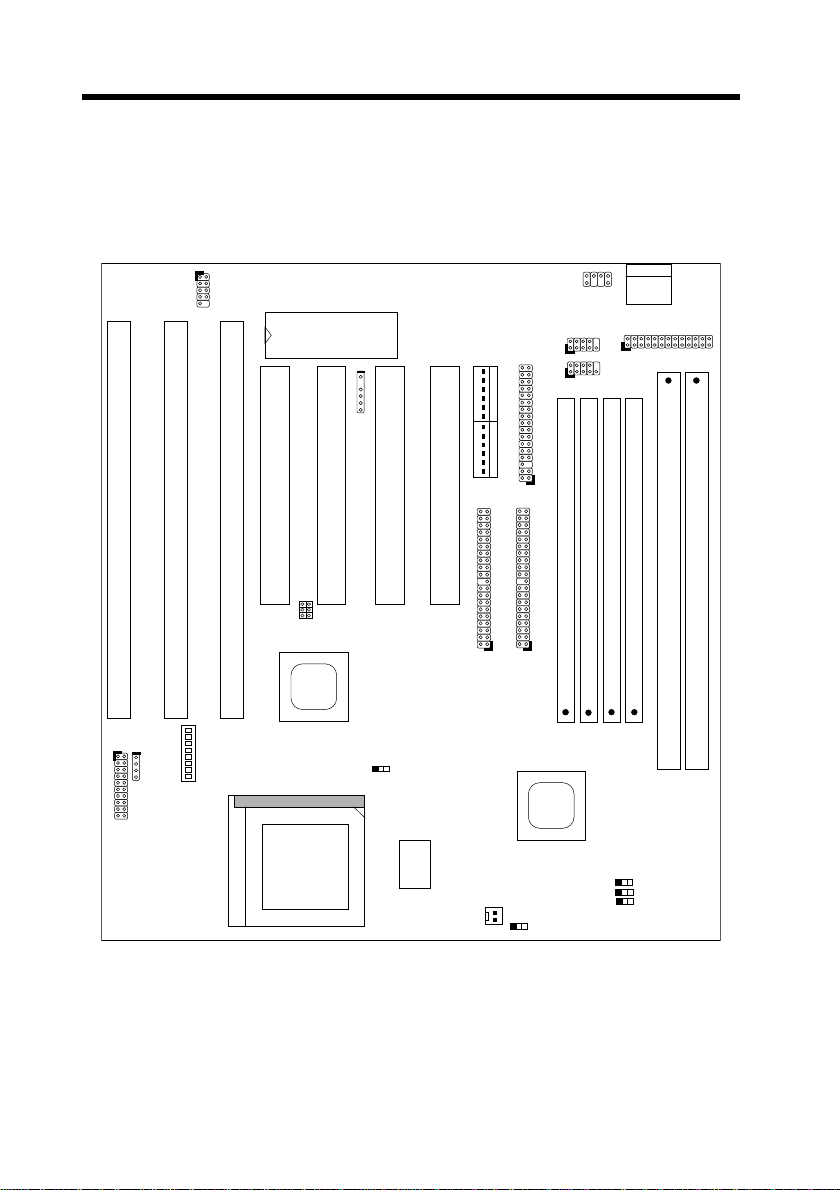
2.1 Jumpers and Connector Locations
The following figure shows the locations of the jumpers and connectors on the
system board:
I
S
A
3
HDD LED
PANEL
USB
KB1
PS2 MS
P
C
I
4
SB-LINK
BIOS
P
C
I
3
IrDA
PWR1
P
P
C
C
I
I
1
2
IDE1
I
I
S
S
A
A
2
1
FDC
IDE2
COM2
COM1
S
I
M
M
1
PRINTER
D
D
I
I
S
S
S
I
I
M
M
M
M
M
M
3
2
M
M
I
M
M
2
1
4
PiiX4
SW1
JP14
TX
JP4
FAN
JP12
JP5
JP6
2-2
Page 20

Hardware Installation
Jumpers
SW1: DIP Switch for CPU voltage and clock ratio
JP4,JP5,JP6: CPU external (bus) clock
JP12: I/O Voltage
JP14: Clear CMOS
Connectors
KB1: AT keyboard connector
PWR1: AT (PS/2) power connector
PS2 MS: PS/2 mouse connector
USB: USB connector
COM1: COM1 connector
COM2: COM2 connector
FDC: Floppy drive connector
PRINTER: Printer connector
IDE1: IDE1 primary channel
IDE2: IDE2 secondary channel
FAN: CPU fan connector
IrDA: IrDA (Infrared) connector
HDD LED: HDD LED connector
PANEL: Front panel (Multifunction) connector
SB-LINK: Creative PCI sound card connector
2-3
Page 21

Hardware Installation
3
3
2.2 Jumpers
Jumpers are made by pin headers and plastic connecting caps for the purpose of
customizing your hardware. Doing so requires basic knowledge of computer
hardware, be sure you understand the meaning of the jumpers before you change
any setting. The onboard jumpers are normally set to their default with optimized
settings.
On the mainboard, normally there is a bold line marked beside pin 1 of the jumper,
sometimes, there are numbers also. If we connect (short) plastic cap to pin 1 and
2, we will say set it at 1-2, and when we say jumper is open, that means no plastic
cap connected to jumper pins.
Open
1
2
Short
1
2
Jumper set at 1-2
1
2
Jumper set at 2-3
1
2
2-4
Page 22
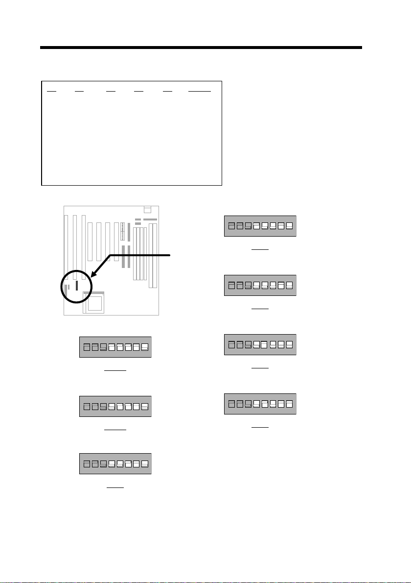
2.2.1 Setting the CPU Voltage
ON
ON
ON
ON
ON
ON
S4
ON
OFF
OFF
ON
OFF
OFF
OFF
S5
ON
ON
OFF
OFF
OFF
ON
ON
S6
ON
ON
ON
OFF
OFF
OFF
OFF
S7
ON
ON
ON
ON
ON
OFF
ON
S8
OFF
OFF
OFF
OFF
OFF
OFF
ON
Vcore
3.52V
3.45V
3.2V
2.9V
2.8V
2.2V
1.8V
Hardware Installation
SW1 is used to select CPU core
voltage (Vcore) and ratio, there
are totally eight switches on the
DIP. After installing a CPU,
remember to set the switch 4-8
to specify a proper Vcore.
1 2 3 4 5 6 7 8
2.9V
K6-166/200 or M2
1 2 3 4 5 6 7 8
2.8V
Intel P55C (MMX)
ON
1 2 3 4 5 6 7 8
3.52V
Cyrix 6x86 or AMD K5
1 2 3 4 5 6 7 8
3.45V
Intel P54C or IDT C6
1 2 3 4 5 6 7 8
1 2 3 4 5 6 7 8
2.2V
K6-266/300
1 2 3 4 5 6 7 8
1.8V
Reserved for future use
3.2V
AMD K6-233
2-5
Page 23

Hardware Installation
Warning: Please make sure that you have installed CPU fan
properly if Intel PP/MT-233 or AMD K6 CPU is being selected
to use. It may cause your system unstable if you can not meet
the heat dissipation requirement from above CPU type. It is
recommended to adopt larger fan on these CPU for better air
flow in the system. Please refer to AOpen 's web site
(http://www.aopen.com.tw) to choose a proper CPU fan.
Tip: Normally, for single voltage CPU, Vcpuio (CPU I/O
Voltage) is equal to Vcore, but for CPU that needs dual voltage
such as PP/MT (P55C) or Cyrix 6x86L, Vcpuio is different from
Vcore and must be set to Vio (PBSRAM and Chipset Voltage).
The single or dual voltage CPU is automatically detected by
hardware circuit.
Tip: For supporting more different CPUs in future, this
motherboard uses five switchs to specify Vcore. There are 32
settings totally, and the range is from 1.3V to 3.5V.
CPU Type S4 S5 S6 S7 S8 Vcore
INTEL P54C Single Voltage OFF ON ON ON OFF 3.45V
INTEL MMX P55C Dual Voltage OFF OFF OFF ON OFF 2.8V
AMD K5 Single Voltage ON ON ON ON OFF 3.52V
AMD K6-166/200 Dual Voltage ON OFF OFF ON OFF 2.9V
AMD K6-233 Dual Voltage OFF OFF ON ON OFF 3.2V
AMD K6-266/300 Dual Voltage OFF ON OFF OFF OFF 2.2V
Cyrix 6x86 Single Voltage ON ON ON ON OFF 3.52V
Cyrix 6x86L Dual Voltage OFF OFF OFF ON OFF 2.8V
Cyrix M2 Dual Voltage ON OFF OFF ON OFF 2.9V
IDT C6 Single Voltage OFF ON ON ON OFF 3.45V
2-6
Page 24

Hardware Installation
This motherboard supports the CPU core voltage from 1.3V to 3.5V, that can be
applied to the various CPU type in future. For your reference, all settings are
listed in the following table.
Vcore
1.30V
1.35V
1.40V
1.45V
1.50V
1.55V
1.60V
1.65V
1.70V
1.75V
1.80V
1.85V
1.90V
1.95V
2.00V
2.05V
2.0V
2.1V
2.2V
2.3V
2.4V
2.5V
2.6V
2.7V
2.8V
2.9V
3.0V
3.1V
3.2V
3.3V
3.4V
3.5V
S4
OFF
ON
OFF
ON
OFF
ON
OFF
ON
OFF
ON
OFF
ON
OFF
ON
OFF
ON
OFF
ON
OFF
ON
OFF
ON
OFF
ON
OFF
ON
OFF
ON
OFF
ON
OFF
ON
S5
OFF
OFF
ON
ON
OFF
OFF
ON
ON
OFF
OFF
ON
ON
OFF
OFF
ON
ON
OFF
OFF
ON
ON
OFF
OFF
ON
ON
OFF
OFF
ON
ON
OFF
OFF
ON
ON
S6
OFF
OFF
OFF
OFF
ON
ON
ON
ON
OFF
OFF
OFF
OFF
ON
ON
ON
ON
OFF
OFF
OFF
OFF
ON
ON
ON
ON
OFF
OFF
OFF
OFF
ON
ON
ON
ON
S7
OFF
OFF
OFF
OFF
OFF
OFF
OFF
OFF
ON
ON
ON
ON
ON
ON
ON
ON
OFF
OFF
OFF
OFF
OFF
OFF
OFF
OFF
ON
ON
ON
ON
ON
ON
ON
ON
S8
ON
ON
ON
ON
ON
ON
ON
ON
ON
ON
ON
ON
ON
ON
ON
ON
OFF
OFF
OFF
OFF
OFF
OFF
OFF
OFF
OFF
OFF
OFF
OFF
OFF
OFF
OFF
OFF
2-7
Page 25
Hardware Installation
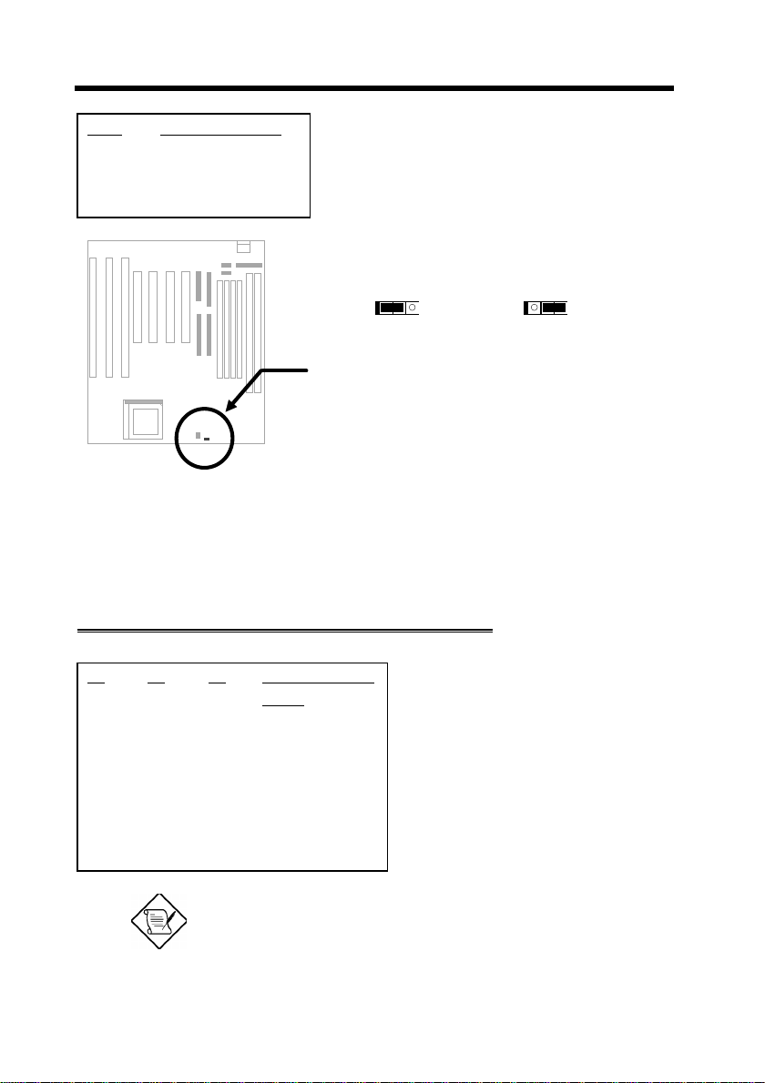
JP12
1-2
3-4
I/O Voltage (Vio)
3.3 (default)
3.45V
JP12 is reserved for testing purposes only.
This jumper enables you to set the voltage of
the onboard chipset and PBSRAM (Vio). For
dual-voltage CPU, JP12 also functions as
CPU I/O voltage (Vcpuio) controller.
JP12
1 2 3
3.3V
(default)
JP12
1 2 3
3.45V
2.2.2 Selecting the CPU Frequency
Intel Pentium, Cyrix 6x86, AMD K5/K6 and IDT C6 CPU are designed to have
different Internal (Core) and External (Bus) frequency.
Core frequency = Ratio * External bus clock
2-8
S1
OFF
ON
ON
OFF
ON
ON
OFF
S2
OFF
OFF
ON
ON
OFF
ON
ON
S3
OFF
OFF
OFF
OFF
ON
ON
ON
CPU Frequency
Ratio
1.5x (3.5x)
2x
2.5x (1.75x)
3x
4x
4.5x
5x
Note: Intel PP/MT MMX 233MHz is using 1.5x jumper setting
for 3.5x frequency ratio, and AMD PR166 is using 2.5x
setting for 1.75x frequency ratio.
The ratio of Core/Bus frequency
is selected by the switch 1-3 of
SW1.
Page 26
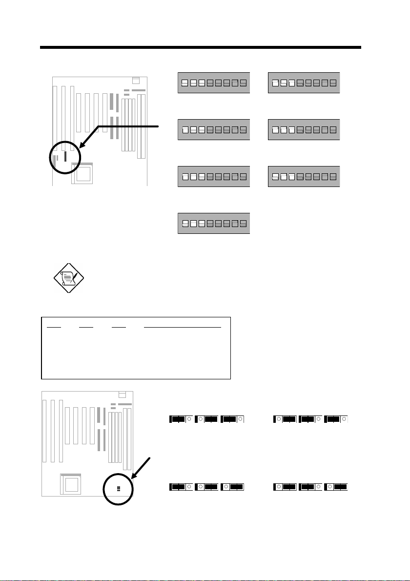
Hardware Installation
ON
ON
ON
ON
ON
ON
ON
JP4
1-2
2-3
1-2
2-3
JP5
2-3
1-2
2-3
1-2
1 2 3 4 5 6 7 8
1.5x (3.5x)
1 2 3 4 5 6 7 8
2x
1 2 3 4 5 6 7 8
2.5x (1.75x)
1 2 3 4 5 6 7 8
1 2 3 4 5 6 7 8
4x
1 2 3 4 5 6 7 8
4.5x
1 2 3 4 5 6 7 8
5x
3x
Note: Intel PP/MT 233MHz is using 1.5x jumper setting for
3.5x frequency ratio, and AMD PR166 is using 2.5x setting for
1.75x frequency ratio.
JP6
1-2
1-2
2-3
2-3
CPU External Clock
60MHz
66MHz
75MHz
83.3MHz
JP4, JP5 and JP6 are the
selections of CPU external
clock (bus clock), which is
actually the clock from clock
generator.
JP4 JP5 JP6
1 2 3 1 2 3 1 2 3
60MHz
JP4 JP5 JP6
1 2 3 1 2 3 1 2 3
75MHz
JP4 JP5 JP6
1 2 3 1 2 3 1 2 3
66MHz
JP4 JP5 JP6
1 2 3 1 2 3 1 2 3
83.3mhz
2-9
Page 27
Hardware Installation
Warning: INTEL TX chipset supports only 60/66MHz
external CPU bus clock, the 75/83.3MHz settings are for
internal test only, set to 75/83.3MHz exceeds the
specification of TX chipset, which may cause serious
system damage.
Caution: Following table are possible settings of current
CPU available on the market. The correct setting may
vary because of new CPU product, refer to your CPU
specification for more details.
Warning: Cyrix 6x86 P200+ uses 75MHz external clock,
the jumper setting shown on the table below is for user's
convenient. It may cause serious system damage to use
75MHz clock.
INTEL
Pentium
P54C 90 90MHz = 1.5x 60MHz OFF OFF OFF 1-2 & 2-3 & 1-2
P54C 100 100MHz = 1.5x 66MHz OFF OFF OFF 2-3 & 1-2 & 1-2
P54C 120 120MHz = 2x 60MHz ON OFF OFF 1-2 & 2-3 & 1-2
P54C 133 133MHz = 2x 66MHz ON OFF OFF 2-3 & 1-2 & 1-2
P54C 150 150MHz = 2.5x 60MHz ON ON OFF 1-2 & 2-3 & 1-2
P54C 166 166MHz = 2.5x 66MHz ON ON OFF 2-3 & 1-2 & 1-2
P54C 200 200MHz = 3x 66MHz OFF ON OFF 2-3 & 1-2 & 1-2
INTEL
Pentium
MMX
PP/MT 150 150MHz = 2.5x 60MHz ON ON OFF 1-2 & 2-3 & 1-2
PP/MT 166 166MHz = 2.5x 66MHz ON ON OFF 2-3 & 1-2 & 1-2
PP/MT 200 200MHz = 3x 66MHz OFF ON OFF 2-3 & 1-2 & 1-2
PP/MT 233 233MHz = 3.5x 66MHz OFF OFF OFF 2-3 & 1-2 & 1-2
AMD K5 CPU Core
PR90 90MHz = 1.5x 60MHz OFF OFF OFF 1-2 & 2-3 & 1-2
PR100 100MHz = 1.5x 66MHz OFF OFF OFF 2-3 & 1-2 & 1-2
PR120 90MHz = 1.5x 60MHz OFF OFF OFF 1-2 & 2-3 & 1-2
PR133 100MHz = 1.5x 66MHz OFF OFF OFF 2-3 & 1-2 & 1-2
PR166 116MHz = 1.75x 66MHz ON ON OFF 2-3 & 1-2 & 1-2
CPU Core
Frequency
CPU Core
Frequency
Frequency
Ratio External
Bus Clock
Ratio External
Bus Clock
Ratio External
Bus Clock
S1 S2 S3 JP4 & JP5 & JP6
S1 S2 S3 JP4 & JP5 & JP6
S1 S2 S3 JP4 & JP5 & JP6
2-10
Page 28
Hardware Installation
AMD K6 CPU Core
PR2-166 166MHz = 2.5x 66MHz ON ON OFF 2-3 & 1-2 & 1-2
PR2-200 200MHz = 3x 66MHz OFF ON OFF 2-3 & 1-2 & 1-2
PR2-233 233MHz = 3.5x 66MHz OFF OFF OFF 2-3 & 1-2 & 1-2
PR2-266 266MHz= 4x 66MHz ON OFF ON 2-3 & 1-2 & 1-2
PR2-300 300MHz= 4.5x 66MHz ON ON ON 2-3 & 1-2 & 1-2
Cyrix 6x86
& 6x86L
P150+ 120MHz = 2x 60MHz ON OFF OFF 1-2 & 2-3 & 1-2
P166+ 133MHz = 2x 66MHz ON OFF OFF 2-3 & 1-2 & 1-2
P200+ 150MHz = 2x 75MHz ON OFF OFF 1-2 & 2-3 & 2-3
Cyrix M2 CPU Core
MX-PR166 150MHz = 2.5x 60MHz ON ON OFF 1-2 & 2-3 & 1-2
MX-PR200 166MHz =
MX-PR233 200MHz =
MX-PR266 233MHz = 3.5x 66MHz OFF OFF OFF 2-3 & 1-2 & 1-2
IDT C6 CPU Core
C6-150 150MHz = 2x 75MHz ON OFF OFF 1-2 & 2-3 & 2-3
C6-180 180MHz = 3x 60MHz OFF ON OFF 1-2 & 2-3 & 1-2
C6-200 200MHz = 3x 66MHz OFF ON OFF 2-3 & 1-2 & 1-2
Frequency
CPU Core
Frequency
Frequency
150MHz=
166MHz=3x2x
Frequency
Ratio External
Ratio External
Ratio External
2.5x
2x
Ratio External
Bus Clock
Bus Clock
Bus Clock
66MHz
75MHz
66MHz
83.3MHz
Bus Clock
S1 S2 S3 JP4 & JP5 & JP6
S1 S2 S3 JP4 & JP5 & JP6
S1 S2 S3 JP4 & JP5 & JP6
ONONON
OFFONON
S1 S2 S3 JP4 & JP5 & JP6
OFF
OFF
OFF
2-3 & 1-2 & 1-2
OFF
1-2 & 2-3 & 2-3
OFF
2-3 & 1-2 & 1-2
OFF
2-3 & 1-2 & 2-3
Note: Cyrix 6x86 and AMD K5 CPU use P-rating for the
reference of CPU benchmark compared with INTEL P54C,
their internal core frequency is not exactly equal to P-rating
marked on the CPU. For example, Cyrix P166+ is 133MHz but
performance is almost equal to P54C 166MHz and AMD
PR133 is 100MHz but performance is almost equal to INTEL
P54C 133MHz.
Note: INTEL TX chipset does not support CPU with 50/55MHz
external bus clock, so that P54C 75MHz, Cyrix P120+,P133+
and AMD PR75 are not supported by this mainboard.
2-11
Page 29
Hardware Installation
2.2.3 Clearing the CMOS
JP14
1-2
2-3
Clear CMOS
Normal operation
(default)
Clear CMOS
You need to clear the CMOS if you forget your
system password. To clear the CMOS, follow
the procedures listed below:
Normal Operation
(default)
The procedure to clear CMOS:
1. Turn off the system power.
2. Locate
3. Return
4. Turn on the system power.
5. Press
JP14 and short pins 2-3 for a few seconds.
JP14 to its normal setting by shorting pins 1-2.
during bootup to enter the BIOS Setup Utility and specify a new
password, if needed.
JP14
1 2 3
JP14
1 2 3
Clear CMOS
2-12
Page 30
Hardware Installation
(+5V)
2.3 Connectors
2.3.1 Power Cable
A standard baby AT (PS/2) power supply has two cables with six wires on each.
Plug in these cables to the onboard power connector in such a way that all the
black wires are in the center. The power connector is marked as PWR1 on the
system board.
Caution: Make sure that the power supply is
off before connecting or disconnecting the
power cable.
Black wire
(GND)
Red wire
PWR1
2-13
Page 31

Hardware Installation
3 1 2 4
2.3.2 CPU Fan
Plug in the fan cable to the two-pin fan connector onboard. The fan
connector is marked CPUFAN on the system board. Attach the heatsink and
fan to the CPU. Check its orientation, make sure the air flow go through the
heatsink.
+12V
GND
CPUFAN
2.3.3 PS/2 Mouse
To connect a PS/2 mouse, insert the
PS/2 mouse bracket connector to PS2
MS
on the system board. Then plug in
the PS/2 mouse cable to the mouse
port on the bracket.
2-14
Pin
1
2
3
4
5
6
5 6
PS2 MS
Description
MS DATA
NC
GND
+5V
MS CLK
NC
Page 32

Hardware Installation
1
1
2.3.4 Serial Devices (COM1/COM2)
To support serial devices, insert the serial device connector into the serial port
on the bracket. Plug in the 10-pin flat cable to the appropriate onboard
connectors. The serial port 1 connector is marked as COM1 and the serial
port 2 connector is marked as COM2 on the system board.
2
2
2.3.5 USB Device (optional)
You need a USB bracket to
have your system to support
additional USB device(s). To
attach a USB bracket, simply
insert the bracket cable to the
onboard USB connector marked
USB.
as
Pin
1
3
5
7
9
COM2
COM1
1
10
10
Description
V0
D0D0+
GND
NC
2
9
9
Pin
Description
2
V1
4
D1-
6
D1+
8
GND
10
NC
9 10
USB
2-15
Page 33

Hardware Installation
1
1
26
2
25
2.3.6 Floppy Drive
Connect the 34-pin floppy drive cable to the floppy drive connector marked as
FDC on the system board.
2
33
34
FDC
2.3.7 Printer
Plug in the 26-pin printer flat cable to the onboard parallel connector
marked as PRINTER on the board.
PRINTER
2-16
Page 34

Hardware Installation
1
1
2.3.8 IDE Hard Disk and CD ROM
This mainboard supports two 40 pin IDE connectors marked as
IDE1 and IDE2. IDE1 is also known as primary channel and
IDE2 as secondary channel, each channel supports two IDE
devices that makes total of four devices.
In order to work together, the two devices on each channel must
be set differently to master and slave mode, either one can be
hard disk or CDROM. The setting as master or slave mode
depends on the jumper on your IDE device, please refer to your
hard disk and CDROM manual accordingly.
Connect your first IDE hard disk to master mode of the primary
channel. If you have second IDE device to install in your
system, connect it as slave mode on the same channel, and the
third and fourth device can be connected on secondary channel
as master and slave mode respectively.
2
40
39
2
40
39
IDE1 IDE2
Caution: The specification of IDE cable is
maximum 46cm (18 inches), make sure your
cable does not excess this length.
Caution: For better signal quality, it is
recommended to set far end side device to
master mode and follow the suggested
sequence to install your new device . Please
refer to following figure.
2-17
Page 35

Hardware Installation
(1st)
(2nd)
4
4
4
IDE1 (Primary Channel)
Slave
IDE2 (Secondary Channel)
Slave
(4th)
2.3.9 Hard Disk LED
The HDD LED connector is marked as HDD LED
on the board. This connector is designed for
different type of housing, actually only two pins are
necessary for the LED. If your housing has four pin
connector, simply plug it in. If you have only two pin
connector, please connect to pin 1-2 or pin 3-4
according to the polarity.
+
1
2
-
3
-
+
HDD LED
4-pin connector
HDD LED
2-pin connector
Pin
1
2
3
4
+
-
-
+
at pin 1-2
Master
(3rd)
1
2
3
Master
Description
HDD LED
GND
GND
HDD LED
+
1
2
-
3
-
+
HDD LED
2-pin connector
at pin 3-4
2-18
Page 36

2.3.10 Panel Connector
+
+
+
+
+
10
20
Hardware Installation
The Panel (multifunction) connector is a 20pin connector marked as PANEL on the
board. Attach the power LED, keylock,
speaker, reset switch, suspend switch, and
green mode LED connectors to the
corresponding pins as shown in the figure.
Some housings have a five-pin connector for
the keylock and power LED Since power
LED and keylock are aligned together, you
can still use this kind of connector.
Keylock
Power LED
Speaker
KEYLOCK
POWER LED
SPEAKER
SPEAKER
1
11
10 20
GND
GND
RESET
+5V
GND
NC
Suspend SW
Reset
1
11
10 20
PANEL
+5V
GND
GREEN LED
GND
SUSPEND SW
SUSPEND SW
GND
NC
RESET
GND
PANEL
Other housings may have a 12-pin
connector. If your housing has this
type of connector, connect it to PANEL
1
11
+5V
as shown in the figure. Make sure that
the red wire of the connector is
connected to +5V.
PANEL
2-19
Page 37

Hardware Installation
KB1
Note: If your housing comes with a Turbo switch, you
may use this connector for Suspend switch function.
Note: Pressing the Suspend switch allows you to
manually force the system to suspend mode.
However, this is possible only if the Power
Management function in the BIOS Setup menu is
enabled.
Warning: If you use toggle mode Turbo switch as
Suspend switch, be sure to push it twice to simulate
momentary mode. Otherwise the system may hang or
fail to reboot.
2.3.11 Keyboard
The onboard keyboard connector is a five-pin AT-compatible connector marked as
KB1. The view angle of drawing shown here is from back panel of the housing.
Note: The mini DIN PS/2 keyboard connector
is optional.
PCB
2-20
Page 38

Hardware Installation
2.3.12 IrDA Connector
Serial port 2 can be configured to support wireless infrared module, with
this module and application software such as Laplink, user can transfer
files to or from laptops, notebooks, PDA and printers. This mainboard
supports IrDA (115Kbps, 1 meter) as well as ASK-IR (19.2Kbps).
Install infrared module onto
IrDA
connector and enable infrared function
from BIOS setup, make sure to have
correct orientation when you plug onto
IrDA connector.
Note: Onboard serial port 2 (COM2) will not be
available after IrDA connector is enabled.
IrDA
Pin
1
2
3
4
5
6
1
2
3
4
5
6
Description
+5V
NC
IRRX
GND
IRTX
NC
2-21
Page 39

Hardware Installation
2.3.13 SB-LINK
SB-LINK is used to connect Creative-compatible
PCI sound card. If you have a Creative-compatible
PCI sound card installed, it is necessary to link the
card to the connector for compatibility issue under
DOS environment.
Pin
1
2
3
4
5
6
1 2
5 6
SB-LINK
Description
GNT#
GND
NC
REQ#
GND
SIRQ#
2-22
Page 40

Hardware Installation
Bank1
Bank0
168
2.4 Installing the System Memory
This mainboard has four 72 pin SIMM
Pin 1 of
DIMM2
Pin 1 of
DIMM1
Pin 1 of
Pin 1 of
The SIMM supported by this mainboard can be identified by 4 kinds of factors:
I. Size: single side, 1Mx32 (4MB), 4Mx32 (16MB), 16Mx32 (64MB), and double
side, 1Mx32x2 (8MB), 4Mx32x2 (32MB), 16Mx32x2 (128MB).
II. Speed: 60ns or 70ns access time
III. Type: FPM (Fast page mode) or EDO (Extended data output)
IV. Parity: without parity (32 bit wide) or with parity (36 bit wide).
The DIMM supported by this motherboard are always 64-bit wide SDRAM, which
can be identified by following factors:
I. Size: single side, 1Mx64 (8MB), 2Mx64 (16MB), 4Mx64 (32MB), 8Mx64
(64MB), 16Mx64 (128MB), and double side, 1Mx64x2 (16MB), 2Mx64x2
(32MB), 4Mx64x2 (64MB), 8Mx64x2 (128MB).
sockets (Single-in-line Memory Module)
and two 168 pin DIMM socket (Dual-inline Memory Module) that allow you to
install system memory from minimum
8MB up to maximum 256MB.
Tip: Here is a trick to check if your DIMM is
single-side or double-side -- if there are traces
connected to golden finger pin 114 and pin 129 of
the DIMM, the DIMM is probably double-side;
otherwise, it is single-side. Following figure is for
your reference.
Pin 129
Pin 114
2-23
Page 41

Hardware Installation
II. Speed: normally marked as -12, which means the clock cycle time is 12ns
and maximum clock of this SDRAM is 83MHz. Sometimes you can also find
the SDRAM marked as -67, which means maximum clock is 67MHz.
III. Buffered and non-buffered: This motherboard supports non-buffered DIMMs.
You can identify non-buffered DIMMs and buffered DIMMs according to the
position of the notch, following figure is for your reference:
Reserved
non-buffered
buffered
Because the positions are different, only non-buffered DIMMs can be inserted into
the DIMM sockets on this motherboard. Although most of DIMMs on current
market are non-buffered, we still recommand you to ask your dealer for the
correct type.
IV. 2-clock and 4-clock signals: Although both of 2-clock and 4-clock signals
are supported by this motherboard, we strongly recommand you to choose 4clock SDRAM in consideration of reliability.
Tip: To identify 2-clock and 4-clock SDRAM, you
may check if there are traces connected to golden
finger pin 79 and pin 163 of the SDRAM. If there
are traces, the SDRAM is probably 4-clock;
Otherewise, it is 2-clock.
V. Parity: This motherboard supports standard 64 bit wide (without parity)
SDRAM.
Because Pentium CPU has 64 bit bus width, the SIMM sockets are arranged in
two banks of two sockets each, they are Bank0 and Bank1. Both SIMMs in each
bank must be in the same size and type. It is allowed to have different speed and
type in different bank, for example, 70ns FPM in one bank and 60ns EDO in
another bank, in such case, each bank is independently optimized for maximum
performance. The memory timing requires at least 70ns fast page mode DRAM
chip, but for optimum performance, 60ns EDO DRAM is recommended.
2-24
Warning: The default memory timing setting is 60ns to
obtain the optimal performance. Because of the
specification limitation, 70ns SIMM is recommended to
be used only for CPU external clock 60MHz.
Page 42

Hardware Installation
There is no jumper setting required for the memory size or type. It is
automatically detected by the system BIOS. You can use any single side SIMM
and DIMM combination list below for BANK0/BANK1 or DIMM socket, and the
total memory size is to add them together. Note that because TX chipset
limitation, the maximum is only 256MB.
SIMM1 SIMM2 Subtotal of
Bank0
None None 0MB None None 0MB
4MB 4MB 8MB 4MB 4MB 8MB
8MB 8MB 16MB 8MB 8MB 16MB
16MB 16MB 32MB 16MB 16MB 32MB
32MB 32MB 64MB 32MB 32MB 64MB
64MB 64MB 128MB 64MB 64MB 128MB
128MB 128MB 256MB 128MB 128MB 256MB
DIMM1 Size of DIMM1 DIMM2 Size of DIMM2
None 0MB None 0MB
8MB 8MB 8MB 8MB
16MB 16MB 16MB 16MB
32MB 32MB 32MB 32MB
64MB 64MB 64MB 64MB
128MB 128MB 128MB 128MB
256MB 256MB 256MB 256MB
SIMM3 SIMM4 Subtotal of
Bank1
Total Memory Size = Subtotal of Bank0 + Subtotal of Bank1
+ Size of DIMM1 + Size of DIMM2
For double side memory module, there is one limitation. This mainboard supports
only 4 RAS# (Row address latch) signals for DRAM control. They can only be
occupied by one DRAM module, they can not be shared. The simple rule is: If
double side module at either Bank0 or DIMM1, the other must be empty. If
you use at DIMM1, Bank0 must be empty. Bank1 and DIMM2 have the same
limitation
.
2-25
Page 43
Hardware Installation
Double side module ateither Bank0 or
DIMM1, the other must be empty.
Double side module at either Bank1 or
DIMM2, theother must beempty.
Following table explains more about the RAS limitation. You can see that Bank0
1st side and DIMM1 2nd side use the same RAS0#, and Bank0 2nd side and
DIMM1 1st side use the same RAS1#. If you are using single side SIMM at Bank0
and single side DIMM at DIMM1, it should be no problem. But only one double
side DIMM or double side SIMM can be at Bank0 or DIMM1.
RAS0#
RAS1#
RAS2#
RAS3#
Bank0
1st
side
X X
Bank0
2nd
side
X X
Bank1
1st
side
X X
Bank1
2nd
side
X X
DIMM1
1st
side
DIMM1
2nd
side
DIMM2
1st
side
DIMM2
2nd
side
Caution: Make sure that you install the same SIMM type and
size for each bank.
Caution: There are some old DIMMs made by EDO or FPM
memory chip, they can only accept 5V power and probably can
not fit into the DIMM socket, make sure you have 3.3V true
SDRAM DIMM before your insert it.
Tip: If you have DIMM made by 3V EDO, it is possible that TX
chipset can support it. But because it is so rare, the only 3V
EDO DIMM had been tested by this mainboard is Micron
MT4LC2M8E7DJ-6.
Warning: Do not use SIMM and SDRAM DIMM together unless
you have 5V tolerance SDRAM (such as Samsung or TI). The
FPM/EDO operate at 5V while SDRAM operates at 3.3V. If you
combine them together the system will temporary work fine;
however after a few months, the SDRAM 3.3V data input will be
damaged by 5V FPM/EDO data output line.
2-26
Page 44

Hardware Installation
There is an important parameter affects SDRAM performance, CAS Latency Time.
It is similar as CAS Access Time of EDO DRAM and is calculated as number of
clock state. The SDRAM that AOpen had tested are listed below. If your SDRAM
has unstable problem, go into BIOS "Chipset Features Setup", change CAS
Latency Time to 3 clocks.
Manufacturer Model Suggested CAS
Latency Time
Samsung KM416511220AT-G12 2 Yes
NEC D4S16162G5-A12-7JF 2 No
Hitachi HM5216805TT10 2 No
Fujitsu 81117822A-100FN 2 No
TI TMX626812DGE-12 2 Yes
TI TMS626812DGE-15 3 Yes
TI TMS626162DGE-15 3 Yes
TI TMS626162DGE-M67 3 Yes
5V Tolerance
The driving capability of new generation chipset is limited because the lack of
memory buffer (to improve performance). This makes DRAM chip count an
important factor to be taking into consideration when you install SIMM/DIMM.
Unfortunately, there is no way that BIOS can identified the correct chip count, you
need to calculate the chip count by yourself. The simple rule is: By visual
inspection, use only SIMM with chip count less than 24 chips, and use only DIMM
which is less than 16 chips.
Warning: Do not install any SIMM that contains more than 24
chips. SIMMs contain more than 24 chips exceed the chipset
driving specification. Doing so may result in unstable system
behavior.
Warning: Although Intel TX chipset supports x4 SDRAM chip.
Due to loading issue, it is not recommended to use this kind of
SDRAM.
Tip: The SIMM/DIMM chip count can be calculated by following
example:
1. For 32 bit non-parity SIMM using 1M by 4 bit DRAM chip,
32/4=8 chips.
2. For 36 bit parity SIMM using 1M by 4 bit DRAM chip,
36/4=9 chips.
3. For 36 bit parity SIMM using 1M by 4 bit and 1M by 1 bit
DRAM, the chip count will be 8 data chips(8= 32/4) plus 4
2-27
Page 45

Hardware Installation
parity chips(4=4/1), total is 12 chips.
4. For 64 bit DIMM using 1M by 16 bit SDRAM, the chip count
is 64/16=4 chips.
Following table list the recommended DRAM combinations of SIMM and DIMM:
SIMM
Data chip
1M by 4 None 1Mx32 x1 8 4MB Yes
1M by 4 None 1Mx32 x2 16 8MB Yes
1M by 4 1M by 1 1Mx36 x1 12 4MB Yes
1M by 4 1M by 4 1Mx36 x1 9 4MB Yes
1M by 4 1M by 4 1Mx36 x2 18 8MB Yes
1M by 16 None 1Mx32 x1 2 4MB Yes
1M by 16 None 1Mx32 x2 4 8MB Yes
1M by 16 1M by 4 1Mx36 x1 3 4MB Yes
1M by 16 1M by 4 1Mx36 x2 6 8MB Yes
4M by 4 None 4Mx32 x1 8 16MB Yes
4M by 4 None 4Mx32 x2 16 32MB Yes
4M by 4 4M by 1 4Mx36 x1 12 16MB Yes
4M by 4 4M by 1 4Mx36 x2 24 32MB Yes
SIMM
Data chip
16M by 4 None 16Mx32 x1 8 64MB Yes, but not
16M by 4 None 16Mx32 x2 16 128MB Yes, but not
16M by 4 16M by 4 16Mx36 x1 9 64MB Yes, but not
16M by 4 16M by 4 16Mx36 x2 18 128MB Yes, but not
SIMM
Parity chip
SIMM
Parity chip
Bit size
per side
Bit size
per side
Single/
Double
side
Single/
Double
side
Chip
count
Chip
count
SIMM
size
SIMM
size
Recommended
Recommended
tested.
tested.
tested.
tested.
DIMM
Data chip
1M by 16 1Mx64 x1 4 8MB Yes
1M by 16 1Mx64 x2 8 16MB Yes
2M by 8 2Mx64 x1 8 16MB Yes
2M by 8 2Mx64 x2 16 32MB Yes
Bit size per
side
Single/
Double side
Chip
count
DIMM size Recommended
2-28
Page 46

Hardware Installation
DIMM
Data chip
2M by 32 2Mx64 x1 2 16MB Yes, but not tested.
2M by 32 2Mx64 x2 4 32MB Yes, but not tested.
4M by 16 4Mx64 x1 4 32MB Yes, but not tested.
4M by 16 4Mx64 x2 8 64MB Yes, but not tested.
8M by 8 8Mx64 x1 8 64MB Yes, but not tested.
8M by 8 8Mx64 x2 16 128MB Yes, but not tested.
Bit size per
side
Single/
Double side
Chip
count
DIMM size Recommended
Warning: 64MB SIMMs using 16M by 4 bit chip (64M bit
technology) are not available in the market and are not
formally tested by AOpen quality test department yet.
However they are supported by design specification from
Intel and they will be tested as soon as they are
available. Note that 64MB SIMMs using 16M by 1 bit
chip (16M bit technology) have chip count exceed 24 and
are strongly not recommended.
Tip: 8 bit = 1 byte, 32 bit = 4 byte. The SIMM size is
represented by number of data byte (whether with or
without parity), for example, the size of single side SIMM
using 1M by 4 bit chip is 1Mx32 bit, that is, 1M x 4 byte=
4MB. For double side SIMM, simply multiply it by 2, that
is, 8MB.
2-29
Page 47

Hardware Installation
Following table are possible DRAM combinations that is NOT recommended:
SIMM
Data chip
1M by 1 None 1Mx32 x1 32 4MB No
1M by 1 1M by 1 1Mx36 x1 36 4MB No
1M by 4 1M by 1 1Mx36 x2 24 8MB No
4M by 1 None 4Mx32 x1 32 16MB No
4M by 1 4M by 1 4Mx36 x1 36 16MB No
16M by 1 None 16Mx32 x1 32 64MB No
16M by 1 16M by 1 16Mx36 x1 36 64MB No
DIMM
Data chip
4M by 4 4Mx64 x1 16 32MB No
4M by 4 4Mx64 x2 32 64MB No
16M by 4 16Mx64 x1 16 128MB No
16M by 4 16Mx64 x2 32 256MB No
SIMM
Parity chip
Bit size per
side
Bit size
per side
Single/
Double side
Single/
Double
side
Chip
count
Chip
count
SIMM
size
DIMM size Recommended
Recommended
Memory error checking is supported by parity check. To use parity check you
need 36 bit SIMM (32 bit data + 4 bit parity), which are automatically detected by
BIOS.
Tip: The parity mode uses 1 parity bit for each byte,
normally it is even parity mode, that is, each time the
memory data is updated, parity bit will be adjusted to
have even count "1" for each byte. When next time, if
memory is read with odd number of "1", the parity error
is occurred and this is called single bit error detection.
2-30
Page 48

Chapter 3
Award BIOS
This chapter tells how to configure the system parameters. You may update
your BIOS via AWARD Flash Utility.
Important: Because the BIOS code is the most
often changed part of the mainboard design, the
BIOS information contained in this chapter
(especially the Chipset Setup parameters) may be
a little different compared to the actual BIOS that
came with your mainboard.
3-1
Page 49

AWARD BIOS
3.1 Entering the Award BIOS Setup Menu
The BIOS setup utility is a segment of codes/routines residing in the BIOS
Flash ROM. This routine allows you to configure the system parameters and
save the configuration into the 128 byte CMOS area, (normally in the RTC chip
or directly in the main chipset). To enter the BIOS Setup, press
POST (Power-On Self Test). The BIOS Setup Main Menu appears as follows.
during
Tip: Choose "Load Setup Defaults" for
recommended optimal performance. Choose
"Load Turbo Defaults" for best performance
with light system loading. Refer to section 3.7.
The section at the bottom of the screen tells how to control the screen. Use
the arrow keys to move between items,
display,
at the bottom of the screen displays a brief description of the highlighted item.
After selecting an item, press
3-2
to exit, and to save the changes before exit. Another section
to select or enter a submenu.
to color scheme of the
Page 50
AWARD BIOS
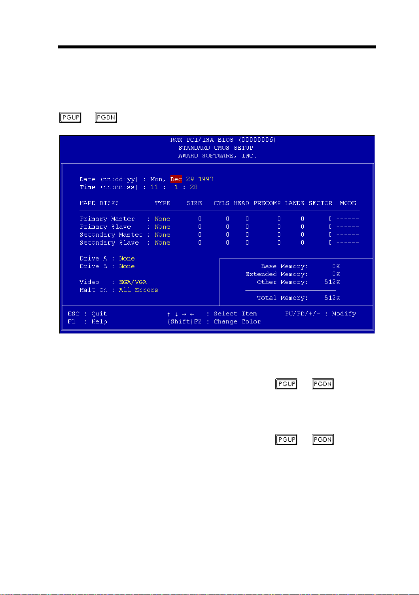
3.2 Standard CMOS Setup
The "Standard CMOS Setup" sets the basic system parameters such as the
date, time, and the hard disk type. Use the arrow keys to highlight an item and
or to select the value for each item.
Standard CMOS à Date
To set the date, highlight the Date parameter. Press
current date. The date format is month, date, and year.
or to set the
Standard CMOS à Time
To set the time, highlight the Time parameter. Press
current time in hour, minute, and second format. The time is based on the 24
hour military clock.
or to set the
3-3
Page 51

AWARD BIOS
Standard CMOS à Primary Master à Type
Standard CMOS à Primary Slave à Type
Standard CMOS
Standard CMOS à Secondary Slave à Type
à
Secondary Master à Type
Type
Auto
User
None
1
2
...
45
Standard CMOS
Standard CMOS
This item lets you select the IDE hard disk parameters
that your system supports. These parameters are Size,
Number of Cylinder, Number of Head, Start Cylinder for
Pre-compensation, Cylinder number of Head Landing
Zone and Number of Sector per Track. The default
setting is Auto, which enables BIOS to automatically
detect the parameters of installed HDD at POST (PowerOn Self Test). If you prefer to enter HDD parameters
manually, select User. Select None if no HDD is
connected to the system.
The IDE CDROM is always automatically detected.
Tip: For an IDE hard disk, we recommend that
you use the "IDE HDD Auto Detection" to enter
the drive specifications automatically. See the
section "IDE HDD Auto Detection".
à
Primary Master à Mode
à
Primary Slave à Mode
Standard CMOS à Secondary Master à Mode
à
Standard CMOS
Mode
Auto
Normal
LBA
Large
Secondary Slave à Mode
The enhanced IDE feature allows the system to use a
hard disk with a capacity of more than 528MB. This is
made possible through the Logical Block Address (LBA)
mode translation. The LBA is now considered as a
standard feature of current IDE hard disk on the market
because of its capability to support capacity larger than
528MB. Note that if HDD is formatted with LBA On, it will
not be able to boot with LBA Off.
3-4
Page 52

Standard CMOS à Drive A
Standard CMOS à Drive B
AWARD BIOS
Drive A
None
360KB 5.25"
1.2MB 5.25"
720KB 3.5"
1.44MB 3.5"
2.88MB 3.5"
Standard CMOS
Video
EGA/VGA
CGA40
CGA80
Mono
Standard CMOS
Halt On
No Errors
All Errors
All, But Keyboard
All, But Diskette
All, But Disk/Key
These items select floppy drive type. The available settings
and types supported by the mainboard are listed on the left.
à
Video
This item specifies the type of video card in use. The
default setting is VGA/EGA. Since current PCs use VGA
only, this function is almost useless and may be
disregarded in the future.
à
Halt On
This parameter enables you to control the system stops in
case of Power-On Self Test (POST) error.
3-5
Page 53

AWARD BIOS
3.3 BIOS Features Setup
This screen appears when you select the option "BIOS Features Setup" from
the main menu.
BIOS Features à Virus Warning
Virus Warning
Enabled
Disabled
Type "Y" to accept write, or "N" to abort write
3-6
Set this parameter to Enabled to activate the warning
message. This feature protects the boot sector and partition
table of your hard disk from virus intrusion.
Any attempt during boot up to write to the boot sector of the
hard disk drive stops the system and the following warning
message appears on the screen. Run an anti-virus program
to locate the problem.
! WARNING !
Disk Boot Sector is to be modified
Award Software, Inc.
Page 54

BIOS Features à External Cache
AWARD BIOS
External Cache
Enabled
Disabled
BIOS Features
Quick Power on
Self test
Enable
Disabled
BIOS Features
Boot Sequence
A,C,SCSI
C,A,SCSI
C,CDROM,A
CDROM,C,A
D,A,SCSI
E,A,SCSI
F,A,SCSI
SCSI,A,C
SCSI,C,A
C only
LS/ZIP,C
Enabling this parameter activates the secondary cache
(currently, PBSRAM cache). Disabling the parameter
slows down the system. Therefore, we recommend that
you leave it enabled unless you are troubleshooting a
problem.
à
Quick Power On Self Test
This parameter speeds up POST by skipping some items
that are normally checked.
à
Boot Sequence
This parameter allows you to specify the system boot up
search sequence. The hard disk ID are listed below:
C: Primary master
D: Primary slave
E: Secondary master
F: Secondary slave
LS: LS120 drive
ZIP: IOMEGA ZIP drive
BIOS Features
Swap Floppy Drive
Enabled
Disabled
à
Swap Floppy Drive
This item allows you to swap floppy drives. For example,
if you have two floppy drives (A and B), you can assign
the first drive as drive B and the second drive as drive A
or vice-versa.
3-7
Page 55

AWARD BIOS
BIOS Features à Boot Up NumLock Status
Boot Up NumLock
Status
On
Off
BIOS Features
Boot Up System
Speed
High
Low
BIOS Features
Typematic Rate
Setting
Enabled
Disabled
BIOS Features
Typematic Rate
6
8
10
12
15
20
24
30
Setting this parameter to On enables the numeric
function of the numeric keypad. Set this parameter to Off
to disregard the function. Disabling the numeric function
allows you to use the numeric keypad for cursor control.
à
Boot Up System Speed
Select High or Low system speed after boot.
à
Typematic Rate Setting
Set this parameter to Enable/Disable the keyboard
repeat function. When enabled, continually holding
down a key on the keyboard will generate repeatedly
keystrokes.
à
Typematic Rate (Chars/Sec)
This item allows you to control the speed of repeated
keystrokes. The default is 30 characters/sec.
BIOS Features
Typematic Delay
250
500
750
1000
3-8
à
Typematic Delay (Msec)
This parameter allows you to control the delay time
between the first and the second keystroke (where the
repeated keystrokes begin). The typematic delay
settings are 250, 500, 750, and 1000 msec.
Page 56

BIOS Features à Security Option
AWARD BIOS
Security Option
Setup
System
BIOS Features
PCI/VGA Palette
Snoop
Enabled
Disabled
The System option limits access to both the System boot
and BIOS setup. A prompt asking you to enter your
password appears on the screen every time you boot the
system.
The Setup option limits access only to BIOS setup.
To disable the security option, select Password Setting
from the main menu, don't type anything and just press
<Enter>.
à
PCI/VGA Palette Snoop
Enabling this item informs the PCI VGA card to keep
silent (and to prevent conflict) when palette register is
updated (i.e., accepts data without responding any
communication signals). This is useful only when two
display cards use the same palette address and plugged
in the PCI bus at the same time (such as MPEQ or Video
capture). In such case, PCI VGA is silent while
MPEQ/Video capture is set to function normally.
BIOS Features à OS Select for DRAM > 64MB
OS Select for
DRAM > 64MB
OS/2
Non-OS/2
Set to OS/2 if your system is utilizing an OS/2
operating system and has a memory size of more than
64 MB.
BIOS Features à Video BIOS Shadow
Video BIOS
Shadow
Enabled
Disabled
VGA BIOS Shadowing means to copy video display
card BIOS into the DRAM area. This enhances system
performance because DRAM access time is faster than
ROM.
3-9
Page 57

AWARD BIOS
BIOS Features à C800-CBFF Shadow
BIOS Features à CC00-CFFF Shadow
BIOS Features
BIOS Features à D400-D7FF Shadow
BIOS Features
BIOS Features à DC00-DFFF Shadow
à
D000-D3FF Shadow
à
D800-DBFF Shadow
C8000-CBFFF
Shadow
Enabled
Disabled
These six items are for shadowing ROM code on other
expansion cards. Before you set these parameters, you
need to know the specific addresses of that ROM code.
If you do not know this information, enable all the ROM
shadow settings.
Note: The F000 and E000 segments are
always shadowed because BIOS code
occupies these areas.
3-10
Page 58

AWARD BIOS
3.4 Chipset Features Setup
The "Chipset Features Setup" includes settings for the chipset dependent
features. These features are related to system performance.
Caution: Make sure you fully understand the
items contained in this menu before you try to
change anything. You may change the
parameter settings to improve system
performance . However, it may cause system
unstable if the setting are not correct for your
system configuration.
3-11
Page 59

AWARD BIOS
Chipset Features à Auto Configuration
Auto Configuration
Enabled
Disabled
Chipset Features
DRAM Timing
60 ns
70 ns
Chipset Features
DRAM Leadoff
Timing
11/7/3/4
10/6/3/3
11/7/4/4
10/6/4/3
When Enabled, the DRAM and cache related timing
are set to pre-defined value according to CPU type
and clock. Select Disable if you want to specify your
own DRAM timing.
à
DRAM Timing
There to sets of DRAM timing parameters can be
automatically set by BIOS, 60ns and 70ns.
Warning: The default memory timing setting
is 60ns to get the optimal performance.
Because the specification limitation of INTEL
TX chipset , 70ns SIMM can only be used
with CPU external clock 60MHz. To use 70ns
SIMM with 66MHz CPU external clock may
result in unstable system behavior.
à
DRAM Leadoff Timing
The Leadoff means the timing of first memory cycle
in the burst read or write. Actually, this item controls
only page miss read/write leadoff timing and the
clocks of RAS precharge and RAS to CAS delay. The
four digital represent Read Leadoff/ Write Leadoff/
RAS Precharge/ RAS to CAS delay. For example,
default is 10/6/3/3, which means you have 10-x-x-x
DRAM page miss read and 6-x-x-x DRAM write, with
3 clocks RAS precharge and 3 clocks RAS to CAS
delay.
3-12
Page 60

Chipset Features à DRAM Read Burst (EDO/FP)
AWARD BIOS
DRAM Read Burst
(EDO/FP)
x444/x444
x333/x444
x222/x333
Read Burst means to read four continuous memory
cycles on four predefined addresses from the DRAM.
The default value is x222/x333 for 60ns EDO or FPM
(Fast Page Mode) DRAM. Which means the 2nd,3rd
and 4th memory cycles are 2 CPU clocks for EDO
and 3 clocks for FPM. The value of x is the timing of
first memory cycle and depends on the "DRAM
Leadoff Timing" setting.
Chipset Features à DRAM Write Burst Timing
DRAM Write Burst
Timing
x444
x333
x222
Chipset Features
Fast EDO Lead Off
Enabled
Disabled
Chipset Features
Write Burst means to write four continuous memory
cycles on four predefined addresses to the DRAM.
This item sets the DRAM write timing of the 2nd,3rd
and 4th memory cycles. There is no difference of
EDO and FPM DRAM on the write burst timing. The
value of x depends on the "DRAM Leadoff Timing"
setting.
à
Fast EDO Lead Off
This item enables fast EDO read timing, results 1
clock pull-in for read leadoff latency of EDO read
cycles. It must be Disabled, if any FPM DRAM is
installed.
à
Refresh RAS# Assertion
Refresh RAS#
Assertion
5 Clks
4 Clks
This item controls the number of clocks RAS is
asserted for refresh cycle.
3-13
Page 61

AWARD BIOS
Chipset Features à DRAM Page Idle Timer
DRAM Page Idle
Timer
2 Clks
4 Clks
6 Clks
8 Clks
Chipset Features
DRAM Enhance
Paging
Enabled
Disabled
This item determines the amount of time in CPU
clocks that DRAM page will be close after CPU
becomes idle.
à
DRAM Enhance Paging
When Enabled, TX chipset will keep DRAM page
open as long as possible according to enhanced
method.
Chipset Features à SDRAM (CAS Lat/RAS-to-CAS)
SDRAM(CAS
Lat/RAS-to-CAS)
2/2
3/3
These are timing of SDRAM CAS Latency and RAS
to CAS Delay, calculated by clocks. They are
important parameters affects SDRAM performance,
default is 2 clocks. If your SDRAM has unstable
problem, change 2/2 to 3/3.
Chipset Features à SDRAM Speculative Read
SDRAM Speculative
Read
Enabled
Disabled
Enable this item reduce one clock of SDRAM read
leadoff timing by presenting the SDRAM read request
before the controller chip decodes the final memory
target. This Item must be Disabled if more than one
DIMM is installed in the system.
Chipset Features
System BIOS
Cacheable
Enabled
Disabled
3-14
à
System BIOS Cacheable
Enabling this item allows you to cache the system
BIOS to further enhance system performance.
Page 62

Chipset Features à Video BIOS Cacheable
AWARD BIOS
Video BIOS
Cacheable
Enabled
Disabled
Chipset Features
8 Bit I/O Recovery
Time
1
2
3
4
5
6
7
8
NA
Chipset Features
16 Bit I/O Recovery
Time
1
2
3
4
NA
Allows the video BIOS to be cached to allow faster
video performance.
à
8 Bit I/O Recovery Time
For some old I/O chips, after the execution of an I/O
command, the device requires a certain amount of
time (recovery time) before the execution of the next
I/O command. Because of new generation CPU and
mainboard chipset, the assertion of I/O command is
faster, and sometimes shorter than specified I/O
recovery time of old I/O devices. This item lets you
specify the delay of 8-bit I/O command by count of
ISA bus clock. If you find any unstable 8-bit I/O card,
you may try to extend the I/O recovery time via this
item. The BIOS default value is 4 ISA clock. If set to
NA, the chipset will insert 3.5 system clocks.
à
16 Bit I/O Recovery Time
The same as 16-bit I/O recovery time. This item lets
you specify the recovery time for the execution of 16bit I/O commands by count of ISA bus clock. If you
find any of the installed 16-bit I/O cards unstable, try
extending the I/O recovery time via this item. The
BIOS default value is 1 ISA clocks. If set to NA, the
chipset will automatically insert 3.5 system clocks.
3-15
Page 63

AWARD BIOS
Chipset Features à Memory Hole At 15M-16M
Memory Hole At
15M-16M
Enabled
Disabled
This option lets you reserve system memory area for
special ISA cards. The chipset accesses code/data
of these areas from the ISA bus directly. Normally,
these areas are reserved for memory mapped I/O
card.
Chipset Features à PCI Passive Release
PCI Passive Release
Enabled
Disabled
Chipset Features
PCI Delayed
Transaction
Enabled
Disabled
This item lets you control the Passive Release
function of the PIIX4 chipset (Intel PCI to ISA bridge).
This function is used to meet latency of ISA bus
master. Try to enable or disable it, if you have ISA
card compatibility problem.
à
PCI Delayed Transaction
This item lets you control the Delayed Transaction
function of the PIIX4 chipset (Intel PCI to ISA bridge).
This function is used to meet latency of PCI cycles to
or from ISA bus. Try to enable or disable it, if you
have ISA card compatibility problem.
Chipset Features à Mem. Drive Str. (MA/RAS)
Mem. Drive Str.
(MA/RAS)
10mA/10mA
10mA/16mA
16mA/10mA
16mA/16mA
This option controls the driving strength of memory
address and control signals. It is recommended to
use less driving current for light memory loading, to
prevent undershoot or overshoot.
3-16
Page 64

3.5 Power Management Setup
AWARD BIOS
The Power Management Setup screen enables you to control the mainboard
green features. See the following screen.
Power Management à Power Management
Power Management
Max Saving
Mix Saving
User Defined
Disabled
This function allows you to set the default parameters
of power-saving modes. Set to Disable to turn off
power management function. Set to User Defined to
choose your own parameters.
’s
Mode Doze Standby Suspend HDD Power Down
Min Saving 1 hour 1 hour 1 hour 15 min
Max Saving 1 min 1 min 1 min 1 min
3-17
Page 65

AWARD BIOS
Power Management à PM Controlled by APM
PM Controlled by
APM
Yes
No
If "Max Saving" is selected, you can turn on this item,
transfer power management control to APM
(Advanced Power Management) and enhance power
saving function. For example, stop CPU internal
clock.
Power Management à Video Off After
Video Off After
N/A
Doze
Standby
Suspend
Power Management
Break Switch
Enabled
Disabled
To turn off video monitor at which power down mode.
à
Break Switch
Setting this item to Enabled allows you to use the
Turbo switch as Suspend switch. Pressing the Turbo
switch changes nothings for a Pentium system, so we
usually use this switch to act as a Suspend switch.
The default value of this item is Disabled.
Warning: If you use toggle mode Turbo switch as
Suspend switch, be sure to push it twice to simulate
momentary mode. Otherwise the system may hang or
fail to reboot.
Power Management
Doze Mode
Disabled
1 Min
2 Min
4 Min
8 Min
12 Min
20 Min
30 Min
40 Min
1 Hour
3-18
à
Doze Mode
This item lets you set the period of time after which
the system enters into Doze mode. In this mode, the
CPU clock slows down. The ratio is specified in the
"Throttle Duty Cycle". Any activity detected returns
the system to full power. The system activity (or
event) is detected by monitoring the IRQ signals.
Page 66

Power Management à Standby Mode
AWARD BIOS
Standby Mode
Disabled
1 Min
2 Min
4 Min
8 Min
12 Min
20 Min
30 Min
40 Min
1 Hour
Power Management
Suspend Mode
Disabled
1 Min
2 Min
4 Min
8 Min
12 Min
20 Min
30 Min
40 Min
1 Hour
This item lets you set the period of time after which
the system enters into Standby mode. In this mode,
CPU clock slows down, hard disk will be shut off and
the monitor power-saving feature activates. Any
activity detected returns the system to full power.
The system activity (or event) is detected by
monitoring the IRQ signals.
à
Suspend Mode
This item lets you set the period of time after which
the system enters into Suspend mode. The Suspend
mode can be Power On Suspend or Suspend to Hard
Drive, selected by "Suspend Mode Option".
Power Management
HDD Power Down
Disabled
1 Min
.....
15 Min
à
HDD Power Down
This option lets you specify the IDE HDD idle time
before the device enters the power down state. This
item is independent from the power states previously
described in this section (Standby and Suspend).
3-19
Page 67

AWARD BIOS
Power Management à Suspend Mode Option
Suspend Mode
Option
Power On Suspend
Suspend to Hard Drive
You can select suspend mode by this item. Power
On Suspend is the traditional Green PC suspend
mode, the CPU clock is stop, all other devices are
shut off. But power must be kept On to detect
activities from modem, keyboard/mouse and returns
the system to full power. The system activities is
detected by monitoring the IRQ signals. Suspend to
Hard Drive saves system status, memory and screen
image into hard disk, then the power can be totally
Off. Next time, when power is turned On, the system
goes back to your original work within just few
seconds. You need AOZVHDD to reserve disk space.
Refer to section 3.16 "Suspend to Hard Drive" for
more information".
Power Management à Throttle Duty Cycle
Throttle Duty Cycle
12.5 %
25.0 %
37.5 %
50.0 %
62.5 %
75.0 %
87.5 %
Clock Throttling means at the Doze/Standby state,
the CPU clock count in a given time (not the
frequency) is reduced to the ratio specified in this
parameter. Actually, the period per CPU clock is not
changed. For example, a 66MHz CPU clock remains
the same 30ns clock period when system goes into
Doze/Suspend. The chipset generates the STPCLK
(stop clock) signal periodically to prevent CPU for
accepting clock from clock generator. For full power
on, the CPU can receive 66M count in one second. If
the Slow Clock Ratio is set to 50%, the CPU will only
receive 33M clock count in one second. This will
effectively reduce CPU speed as well as CPU power.
Power Management
VGA Activity
Monitor
Enabled
Disabled
3-20
à
VGA Activity Monitor
To enable or disable the detection of VGA activity for
power down state transition.
Page 68

Power Management à IRQ 8 Clock Event
AWARD BIOS
IRQ 8 Clock Event
Enabled
Disabled
Power Management
IRQ [3-7,9-15], NMI
Enabled
Disabled
Power Management
Power Management
Power Management
To enable or disable the detection of IRQ8 (RTC)
event for power down state transition. OS2 has
periodically IRQ8 (RTC) interruptions, If IRQ8 is not
set to Disabled, OS/2 may fail to go into
Doze/Standby/Suspend mode.
à
IRQ [3-7,9-15], NMI
To enable or disable the detection of IRQ3-7, IRQ915 or NMI interrupt events for power down state
transition.
à
Primary IDE 0
à
Primary IDE 1
à
Secondary IDE 0
Power Management à Secondary IDE 1
à
Power Management
Floppy Disk
Power Management à Serial Port
Power Management
Primary IDE 0
Enabled
Disabled
à
Parallel Port
These items enable or disable the detection of IDE,
floppy, serial and parallel port activities for power
down state transition. Actually it detects the
read/write to/from I/O or address port.
3-21
Page 69

AWARD BIOS
3.6 PNP/PCI Configuration Setup
The PNP/PCI Configuration Setup allows you to configure the ISA and PCI
devices installed in your system. The following screen appears if you select
the option "PNP/PCI Configuration Setup" from the main menu.
PNP/PCI Configuration à PnP OS Installed
PnP OS Installed
Yes
No
3-22
Normally, the PnP resources are allocated by BIOS
during POST (Power-On Self Test). If you are using
a PnP operating system (such as Windows 95), set
this item to Yes to inform BIOS to configure only the
resources needed for booting (VGA/IDE or SCSI).
The rest of system resources will be allocated by PnP
operating system.
Page 70

AWARD BIOS
PNP/PCI Configuration à Resources Controlled By
Resources Controlled
by
Auto
Manual
PNP/PCI Configuration
Reset Configuration
Data
Enabled
Disabled
PNP/PCI Configuration
PNP/PCI Configuration
Setting this option to Manual allows you to
individually assign the IRQs and DMAs to the ISA
and PCI devices. Set this to Auto to enable the autoconfiguration function.
à
Reset Configuration Data
In case conflict occurs after you assign the IRQs or
after you configure your system, you can enable this
function, allow your system to automatically reset
your configuration and reassign the IRQs.
à
IRQ3 (COM2)
à
IRQ4 (COM1)
PNP/PCI Configuration à IRQ5 (Network/Sound or Others)
PNP/PCI Configuration
à
IRQ7 (Printer or Others)
PNP/PCI Configuration à IRQ9 (Video or Others)
PNP/PCI Configuration
à
IRQ10 (SCSI or Others)
PNP/PCI Configuration à IRQ11 (SCSI or Others)
à
PNP/PCI Configuration
IRQ12 (PS/2 Mouse)
PNP/PCI Configuration à IRQ14 (IDE1)
PNP/PCI Configuration à IRQ15 (IDE2)
IRQ 3
Legacy ISA
PCI/ISA PnP
If your ISA card is not PnP compatible and requires a
special IRQ to support its function, set the selected IRQ to
Legacy ISA. This setting informs the PnP BIOS to reserve
the selected IRQ for the installed legacy ISA card. The
default is PCI/ISA PnP. Take note that PCI cards are
always PnP compatible (except old PCI IDE card).
3-23
Page 71

AWARD BIOS
PNP/PCI Configuration à DMA 0
PNP/PCI Configuration à DMA 1
PNP/PCI Configuration
PNP/PCI Configuration à DMA 5
PNP/PCI Configuration
PNP/PCI Configuration à DMA 7
à
DMA 3
à
DMA 6
DMA 0
Legacy ISA
PCI/ISA PnP
If your ISA card is not PnP compatible and requires a
special DMA channel to support its function, set the
selected DMA channel to Legacy ISA. This setting informs
the PnP BIOS to reserve the selected DMA channel for the
installed legacy ISA card. The default is PCI/ISA PnP.
Take note that PCI card does not require DMA channel.
PNP/PCI Configuration à PCI IDE IRQ Map To
PCI IDE IRQ Map
To
ISA
PCI-Slot1
PCI-Slot2
PCI-Slot3
PCI-Slot4
PCI-Auto
PNP/PCI Configuration
PNP/PCI Configuration
Primary IDE INT#
A
B
C
D
Some old PCI IDE add-on cards are not fully PnP
compatible. These cards require you to specify the
slot in use to enable BIOS to properly configure the
PnP resources. This function allows you to select the
PCI slot for any PCI IDE add-on card present in your
system. Set this item to Auto to allow BIOS to
automatically configure the installed PCI IDE card(s).
à
Primary IDE INT#
à
Secondary IDE INT#
These two items, in conjunction with item "PCI IDE
IRQ Map To", specify the IRQ routing of the primary
or secondary channel of the PCI IDE add-on card
(not the onboard IDE). Each PCI slot has four PCI
interrupts aligned as listed in the table below. You
must specify the slot in the "PCI IDE IRQ Map To",
and set the PCI interrupt (INTx) here according to the
interrupt connection on the card.
PCI Slot Location 1
(pin A6)
3-24
Location 2
(pin B7)
Location 3
(pin A7)
Location 4
(pin B8)
Page 72

AWARD BIOS
Slot 1 INTA INTB INTC INTD
Slot 2 INTB INTC INTD INTA
Slot 3 INTC INTD INTA INTB
Slot 4 INTD INTA INTB INTC
Slot 5 (if any) INTD INTA INTB INTC
PNP/PCI Configuration
Used MEM base addr
N/A
C800
CC00
D000
D400
D800
DC00
à
Used MEM Base Addr
This item, in conjunction with the "Used MEM
Length", lets you set a memory space for non-PnP
compatible ISA card. This item specifies the
memory base (start address) of the reserved
memory space. The memory size is specified in the
"Used MEM Length".
PNP/PCI Configuration à Used MEM Length
Used MEM Length
8K
16K
32K
64K
If your ISA card is not PnP compatible and requires
special memory space to support its function,
specify the memory size in this parameter to inform
the PnP BIOS to reserve the specified memory
space for installed legacy ISA card.
3-25
Page 73

AWARD BIOS
3.7 Load Setup Defaults
The "Load Setup Defaults" option loads optimized settings for optimum system
performance. Optimal settings are relatively safer than the Turbo settings.
We recommend you to use the Optimal settings if your system has large
memory size and fully loaded with add-on card (for example, a file server using
double-sided 8MB SIMM x4 and SCSI plus Network card occupying the PCI
and ISA slots).
Optimal is not the slowest setting for this mainboard. If you need to verify a
unstable problem, you may manually set the parameter in the "BIOS Features
Setup" and "Chipset Features Setup" to get slowest and safer setting.
3.8 Load Turbo Defaults
The "Load Turbo Defaults" option gives better performance than Optimal
values. However, Turbo values may not be the best setting of this mainboard
but these values are qualified by the AOpen RD and QA department as the
reliable settings especially if you have limited loading of add-on card and
memory size (for example, a system that contains only a VGA/Sound card and
two SIMMs).
To attain the best system performance, you may manually set the parameters
in the "Chipset Features Setup" to get proprietary setting. Make sure that you
know and understand the functions of every item in Chipset Setup menu. The
performance difference of Turbo from Optimal is normally around 3% to 10%,
depending on the chipset and the application.
3-26
Page 74

AWARD BIOS
3.9 Integrated Peripherals
The following screen appears if you select the option "Integrated Peripherals"
from the main menu. This option allows you to configure the I/O features.
Integrated Peripherals à IDE HDD Block Mode
IDE HDD Block
Mode
Enabled
Disabled
This feature enhances disk performance by allowing
multisector data transfers and eliminates the interrupt
handling time for each sector. Most IDE drives,
except with old designs, can support this feature.
3-27
Page 75

AWARD BIOS
Integrated Peripherals à IDE Primary Master PIO
Integrated Peripherals à IDE Primary Slave PIO
Integrated Peripherals
Integrated Peripherals à IDE Secondary Slave PIO
à
IDE Secondary Master PIO
IDE Primary Master
PIO
Auto
Mode 1
Mode 2
Mode 3
Mode 4
Integrated Peripherals
Setting this item to Auto activates the HDD speed
auto-detect function. The PIO mode specifies the
data transfer rate of HDD. For example: mode 0
data transfer rate is 3.3MB/s, mode 1 is 5.2MB/s,
mode 2 is 8.3MB/s, mode 3 is 11.1MB/s and mode 4
is 16.6MB/s. If your hard disk performance becomes
unstable, you may manually try the slower mode.
Caution: It is recommended that you connect
the first IDE device of each channel to the
endmost connector of the IDE cable. Refer to
section 2.3 "Connectors" for details on how to
connect IDE device(s).
à
IDE Primary Master UDMA
Integrated Peripherals à IDE Primary Slave UDMA
Integrated Peripherals
à
IDE Secondary Master UDMA
Integrated Peripherals à IDE Secondary Slave UDMA
IDE Primary Master
UDMA
Auto
Disabled
This item allows you to set the Ultra DMA/33 mode
supported by the hard disk drive connected to your
primary IDE connector.
Integrated Peripherals à On-Chip Primary PCI IDE
à
Integrated Peripherals
On-Chip Secondary PCI IDE
On-Chip Primary
PCI IDE
Enabled
Disabled
3-28
This parameter lets you enable or disable the IDE
device connected to the primary IDE connector.
Page 76

Integrated Peripherals à USB Legacy Support
AWARD BIOS
USB Legacy Support
Enabled
Disabled
Caution: You can not use both USB driver
and USB legacy keyboard at the same time.
Disable "USB Legacy Support" if you have
USB driver in the operating system.
Integrated Peripherals
USB IRQ Released
Yes
No
Note: Normally, PCI VGA does not need PCI
interrupt, you may put PCI VGA on slot4.
Integrated Peripherals
Onboard FDC
Controller
Enabled
Disabled
This item lets you enable or disable the USB
keyboard driver within the onboard BIOS. The
keyboard driver simulates legacy keyboard command
and let you use USB keyboard during POST or after
boot if you don't have USB driver in the operating
system.
à
USB IRQ Released
USB device is default to use PCI INTD#, the same as
PCI slot4. If you installed PCI card on slot4 and
require to use INTD#, set this item to Yes. The USB
device will then be disabled.
à
Onboard FDC Controller
Setting this parameter to Enabled allows you to
connect your floppy disk drives to the onboard floppy
disk connector instead of a separate controller card.
Change the setting to Disabled if you want to use a
separate controller card.
3-29
Page 77

AWARD BIOS
Integrated Peripherals à Onboard Serial Port 1
Integrated Peripherals à Onboard Serial Port 2
Onboard Serial Port 1
Auto
3F8/IRQ4
2F8/IRQ3
3E8/IRQ4
2E8/IRQ3
Disabled
Integrated Peripherals
Onboard UART 2
Mode
Standard
HPSIR
ASKIR
This item allow you to assign address and interrupt
for the board serial port. Default is Auto.
Note: If you are using an network card, make
sure that the interrupt does not conflict.
à
Onboard UART 2 Mode
This item is configurable only if the "Onboard
UART 2" is enabled. This allows you to specify
the mode of serial port2. The available mode
selections are:
• Standard - Sets serial port 2 to operate in normal mode. This is the
default setting.
• HPSIR - Select this setting if you installed an Infrared module in your
system via IrDA connector (refer to section 2.3 "Connectors"). This
setting allows infrared serial communication at a maximum baud rate of
115K baud.
• ASKIR - Select this setting if you installed an Infrared module via IrDA
connector (refer to section 2.3 "Connectors"). This setting allows infrared
serial communication at a maximum baud rate of 19.2K baud.
3-30
Page 78

Integrated Peripherals à Onboard Parallel Port
AWARD BIOS
Onboard Parallel
Port
3BC/IRQ7
378/IRQ7
278/IRQ5
Disabled
Integrated Peripherals
Parallel Port Mode
SPP
EPP
ECP
ECP + EPP
This item controls the onboard parallel port address
and interrupt.
Note: If you are using an I/O card with a
parallel port, make sure that the addresses
and IRQ do not conflict.
à
Parallel Port Mode
This item lets you set the parallel port mode. The
mode options are SPP (Standard Parallel Port), EPP
(Enhanced Parallel Port) and ECP (Extended Parallel
Port). SPP is the IBM AT and PS/2 compatible
mode. EPP enhances the parallel port throughput by
directly writing/reading data to/from parallel port
without latch. ECP supports DMA and RLE (Run
Length Encoded) compression and decompression.
Integrated Peripherals à ECP Mode Use DMA
ECP Mode Use DMA
3
1
This item lets you set the DMA channel of ECP
mode.
Integrated Peripherals à CPU Thermal (Temp.)
CPU Thermal
(Temp.)
Ignore
Monitor
This function lets you control the Thermal Detection
function. When you set this option to Monitor and the
temperature of CPU exceeds predefined value, then:
1. The PC speaker will beep 5 times.
2. The CPU cycle timer will descend about 35%.
Note:The CPU cycle timer won't be restored
to the original status until you reset the
system.
3-31
Page 79

AWARD BIOS
3.10 Password Setting
Password prevents unauthorized use of your computer. If you set a password,
the system prompts for the correct password before boot or access to Setup.
To set a password:
1. At the prompt, type your password. Your password can be up to 8
alphanumeric characters. When you type the characters, they appear as
asterisks on the password screen box.
2. After typing the password, press <Enter> key.
3. At the next prompt, re-type your password and press again to confirm
the new password. After the password entry, the screen automatically
reverts to the main screen.
To disable the password, press when prompted to enter the password. The
screen displays a message confirming that the password has been disabled.
3.11 IDE HDD Auto Detection
If your system has an IDE hard drive, you can use this function to detect its
parameters and enter them into the "Standard CMOS Setup" automatically.
This routine only detects one set of parameters for your IDE hard drive. Some
IDE drives can use more than one set of parameters. If your hard disk is
formatted using different parameters than those detected, you have to enter
the parameters manually. If the parameters listed do not match the ones used
to format the disk, the information on that disk will not be accessible. If the
auto-detected parameters displayed do not match those that used for your
drive, ignore them. Type N to reject the values and enter the correct ones
manually from the Standard CMOS Setup screen.
3.12 Save & Exit Setup
This function automatically saves all CMOS values before leaving Setup.
3-32
Page 80

AWARD BIOS
3.13 Exit without Saving
Use this function to exit Setup without saving the CMOS value changes. Do
not use this option if you want to save the new configuration.
3.14 NCR SCSI BIOS and Drivers
The NCR 53C810 SCSI BIOS resides in the same flash memory chip as the
system BIOS. The onboard NCR SCSI BIOS is used to support NCR 53C810
SCSI control card without BIOS code.
The NCR SCSI BIOS directly supports DOS, Windows 3.1 and OS/2. For
better system performance, you may use the drivers that come with the NCR
SCSI card or with your operating system. For details, refer to the installation
manual of your NCR 53C810 SCSI card.
3-33
Page 81

AWARD BIOS
3.15 BIOS Flash Utility
The BIOS Flash utility allows you upgrade the system BIOS. To get the
AOpen Flash utility and the upgrade BIOS file, contact your local distributor or
visit our homepage at http://www.aopen.com.tw. Please make sure that you
have the correct BIOS ready, the BIOS filename is normally like
AP5TC110.BIN, which means model AP5TC BIOS revision 1.10.
There are two useful programs, Checksum utility CHECKSUM.EXE and
AOpen Flash utility AOFLASH.EXE. Follow the procedures below to upgrade
your BIOS.
[CHECKSUM.EXE]
This utility will help you to determine if the BIOS has been downloaded
correctly or not.
1. Execute
C:> CHECKSUM Biosfile.bin
(Where Biosfile.bin indicates the file name of the BIOS code.)
2. The utility will show "Checksum is ssss".
3. Compare the "ssss" with original checksum posted on Web or BBS. If they
are different, please do not proceed any further and try to download the
BIOS again.
[AOFLASH.EXE]
This utility will try to check the mainboard model, BIOS version and Super/Ultra
IO chip model. To ensure the correct BIOS file for the correct mainboard and
IO chip. This utility will permanently replace your original BIOS content after
flashing.
1. Bootup the system from DOS prompt without loading any memory manager
(HIMEM, EMM386, QEMM386, ...).
2. Execute
C:> AOFLASH Biosfile.bin
(Where Biosfile.bin indicates the file name of the BIOS code.)
3. After loading the new BIOS code, the utility will prompt you to save original
BIOS code into your HDD or floppy. Please press "Y" to store it as
"BIOS.OLD".
4. After the old BIOS has been successfully saved, press "Y" to replace BIOS.
3-34
Page 82

AWARD BIOS
5. DO NOT turn off the power during "FLASHING".
6. Reboot the system by turn off the power after "FLASHING".
7. Press "DEL" key to enter BIOS setup during POST.
8. Reload the "BIOS SETUP DEFAULT" and reconfigure other items as
previous set.
9. Save & Exit. Done!
Warning: DO NOT turn off the power during
"FLASHING". If the BIOS programming is not
successfully finished, the system will not be boot
again, and you may need to physically replace the
BIOS chip.
Tip: You may load back original BIOS "BIOS.OLD"
by the same procedure.
3-35
Page 83

Appendix A
BIOS revision
AP5T revision 3.4
Rev 3.4
Frequently Asked Question
Note: FAQ may be updated without notice. If
you cannot find the information that you need in
this appendix, visit our WWW home page,
(address: http://www.aopen.com.tw) and check
the FAQ area and other new information.
Q: How can I identify the mainboard BIOS version?
A: The AOpen mainboard BIOS version appears on the upper-left corner of
the POST (Power-On Self Test) screen. Normally, it starts with R and is
found in between the model name and the date. For example:
AP53/AX53 R3.80 Oct.22.1996
Q: How can I identify version of the mainboard?
A: The AOpen mainboard revision appears as Rev x.x on the PCB, near the
PCI slot. For example, for AP5T revision 3.4, the revision number appears
on the PCB as follows:
AP5T MB
A-1
Page 84

Frequently Asked Questions
Q: Why the AOpen mainboards (MB) do not have cache module
expansion slot?
A: Faster CPU speed requires more difficult and complex MB timing design.
Every trace and components delay must be taken into consideration. The
expansion cache slot design will cause 2 or 3ns delay in PBSRAM timing,
and the extended trace length to the cache module through the golden
finger will further delay the timing by 1 or 2ns. This may result in unreliable
system once the cache module and slot becomes worn. All AOpen MBs
support 512KB PBSRAM onboard. For better performance (around 3%
higher than 256KB), we strongly recommend you to use 512KB onboard.
Otherwise, reliable 256KB is better than unreliable 512KB with cache
module. AOpen is the first company to promote this concept since the
fourth quarter of 1995.
Q: What is FCC DoC (Declaration of Conformity)?
A: The DoC is new certification standard of FCC regulations. This new
standard allows DIY component (such as mainboard) to apply DoC label
separately without a shielding of housing. The rule to test mainboard for
DoC is to remove housing and test it with regulation 47 CFR 15.31. The
DoC test of mainboard is more difficult than traditional FCC test. If the
mainboard passes DoC test, that means it has very low EMI radiation and
you can use any kind of housing (even paper housing). Following is an
example of DoC label.
AP5T
Test To Comply
With FCC Standards
FOR HOME OR OFFICE USE
Q: Can SDRAM DIMM work together with FPM/EDO SIMM?
A: The FPM/EDO operate at 5V while SDRAM operates at 3.3V. The current
MB design provides different power to DIMM and SIMM but connects the
data bus together. If you combine SIMM and DIMM, the system will still
work fine; however, only temporarily. After a few months, the SDRAM 3.3V
data input will be damaged by 5V FPM/EDO data output line. Therefore,
we strongly NOT recommend DIMM and SIMM combined together. There
is one exception, if your SDRAM supports 5V tolerance (such as TI or
Samsung), which accepts 5V signal at 3.3V operating power, you can
combine them.
A-2
Page 85

Frequently Asked Question
Manufacturer Model Suggested CAS
Latency Time
Samsung KM416511220AT-
G12
NEC D4S16162G5-A12-7JF 2 No
Hitachi HM5216805TT10 2 No
Fujitsu 81117822A-100FN 2 No
TI TMX626812DGE-12 2 Yes
TI TMS626812DGE-15 3 Yes
TI TMS626162DGE-15 3 Yes
TI TMS626162DGE-M67 3 Yes
Q: What is Bus Master IDE (DMA mode)?
A: The traditional PIO (Programmable I/O) IDE requires the CPU to involve in
all the activities of the IDE access including waiting for the mechanical
events. To reduce the workload of the CPU, the bus master IDE device
transfers data from/to memory without interrupting CPU, and releases CPU
to operate concurrently while data is transferring between memory and IDE
device. You need the bus master IDE driver and the bus master IDE HDD
to support bus master IDE mode. Note that it is different with master/slave
mode of the IDE device connection. For more details, refer to section 2.3
"Connectors".
2 Yes
5V Tolerance
Q: What is 3.3V Over-current Protection?
A: The Over-current Protection was very popular implemented on the Baby AT
or ATX +5V/+12V switching power supply. It is very useful to prevent
accident short circuit when you install the mainboard, HDD, add-on cards
into housing. But unfortunately, the new generation CPU and chipset use
3.3V or 2.8V voltage which has regulator to transfer 5V to 3.3V/2.8V, and
makes 5V over-current protection useless. AOpen TX mainboard
AP5T/AX5T with switching regulator onboard support 3.3V (Vcpuio,
chipset, PBSRAM, SDRAM) and 2.8V (CPU Vcore) over-current protection,
in conjunction with 5V/12V power supply provide the full line over-current
protection.
Q: What is CPU Thermal Protection?
A: The higher speed of CPU , the more heat dissipation need to be taking into
consideration. If user does not use correct fan for the CPU cooling, it is
highly possible the CPU can over heat and causing system unstable.
AOpen AP5T/AX5T/AX6F has special thermal detection circuit under the
A-3
Page 86

Frequently Asked Questions
CPU, and slow down the CPU speed as well as warning when temperature
is high then a predefined temperature. (Normally, 55 degree C.)
Q: What is the Ultra DMA/33?
A: This is the new specification to improve IDE HDD data transfer rate. Unlike
traditional PIO mode, which only uses the rising edge of IDE command
signal to transfer data, the DMA/33 uses both rising edge and falling edge.
Hence, the data transfer rate is double of the PIO mode 4 or DMA mode 2.
(16.6MB/s x2 = 33MB/s).
The following table lists the transfer rate of IDE PIO and DMA modes. The
IDE bus is 16-bit, which means every transfer is two bytes.
Mode Clock per
33MHz
PCI
PIO mode 0 30ns 20 600ns (1/600ns) x 2byte = 3.3MB/s
PIO mode 1 30ns 13 383ns (1/383ns) x 2byte = 5.2MB/s
PIO mode 2 30ns 8 240ns (1/240ns) x 2byte = 8.3MB/s
PIO mode 3 30ns 6 180ns (1/180ns) x 2byte = 11.1MB/s
PIO mode 4 30ns 4 120ns (1/120ns) x 2byte = 16.6MB/s
DMA mode 0 30ns 16 480ns (1/480ns) x 2byte = 4.16MB/s
DMA mode 1 30ns 5 150ns (1/150ns) x 2byte = 13.3MB/s
DMA mode 2 30ns 4 120ns (1/120ns) x 2byte = 16.6MB/s
DMA/33 30ns 4 120ns (1/120ns) x 2byte x2 = 33MB/s
Clock
count
Cycle
time
Data Transfer rate
A-4
Page 87

Frequently Asked Question
Q: What is the performance of Ultra DMA/33? Do we need special driver?
A: You need driver to activate DMA/33, there are now driver from INTEL or
you can use driver in the Windows 95 Memphis, which can recognize
South Bridge PIIX4.
We got the mass production sample Quantum Fireball ST1.6A, following
are the test result.
MB : AOpen AP5T
CPU : P54C-200 Mhz
DRAM : 16MB * 2 (FP-7)
VGA : AOpen PV60
CDROM : AOpen CD-920E (20X)
OS : Win95 OSR2
Model OS/Driver Mode Winbench97
Disk Winmark
(Business)
Quantum
Fireball
1.2G
Quantum
Fireball
1.2G
Quantum
ST1.6A
Quantum
ST1.6A
Windows 95
OSR2
Windows 95
OSR2 + INTEL
PIIX4 driver
Windows 95
OSR2
Windows 95
OSR2 + INTEL
PIIX4 driver
PIO mode 4 717 2150
DMA mode 2 822 3050
PIO mode 4 853 2630
DMA/33 1040 4020
Winbench97
Disk Winmark
(High End)
A-5
Page 88

Frequently Asked Questions
Q: What is the memory performance improvement of TX chipset?
A: Following is the compare table of TX+SDRAM, VX+SDRAM, TX+EDO,
HX+EDO and VX+EDO.
CPU : Pentium PP/MT (P55C) 200MHz
DRAM :16MB EDO or SDRAM
HDD : Quantum Fireball 1280AT
VGA : AOpen PV60 S3 Trio64V+ 800x600x256 Small font
OS : Windows 95 OSR2
Chipset Model DRAM Timing Winstone9
6
Intel 430VX AP5VM EDO 6-2-2-2 86.1
Intel 430HX AP53/AP5K EDO 5-2-2-2 86.8
Intel 430TX AP5T/AX5T EDO 5-2-2-2 87.3
Intel 430VX AP5VM/AP5V SDRAM 6-1-1-1 86.6
Intel 430TX AP5T/AX5T SDRAM 5-1-1-1 87.7
Q: Power Management Icon does not appear in the Windows 95 Control
Panel even though the APM under BIOS Setup is enabled.
A: This problem occurs if you did not enable the APM function before you
install Windows 95. If you have already installed Windows 95, re-install it
after the BIOS APM function is enabled.
A-6
Page 89

Frequently Asked Question
Q: Why does the system fail to go into suspend mode under Win95?
A: This problem may be caused by your CDROM settings. The CDROM Auto
Insert Notification of Win95 is dafault enabled, the system will continue to
monitor your CDROM, auto-execute application when a CD diskette is
loaded, and prevents the system from entering into suspend mode. To
resolve this, go into Control Panel è System è Device Manager è
CDROM è Setting, and disable the "Auto Insert Notification" function.
Q: How can I eliminate the "?" marks presented under Device Manager
after installing Win'95 on TX or LX based system?
A: Although your system will still work fine with this "?" exist. We received
many requests about how to eliminate it. AOpen software team spends few
weeks to develop an utility AOchip.exe for convenience of Win95 users. It
is very user friendly and can be used on any TX or LX motherboard, not
limited to Aopen's products. You are welcome to distribute it, if you like it,
simply say thanks to our software team. Note that you need USB driver for
USB devices to work properly, which is expected to be implemented on
Windows'98.
Q: Why are there question marks or "standard IDE controller" presented
under Device Manager after installing Win'95 on TX or LX based system?
A: Intel has introduced 430TX or 440LX chipset with latest feature of "ACPI",
"USB" & "Ultra DMA/33". Since these devices are so new that Win'95 did
not anticipate to support them on Aug. of '95 which Win'95 initially is being
released. To eliminate, you may run AOchip.exe developed by AOpen
software team. Drivers for above new features are expected to be
implemented in Windows'98.
A-7
Page 90

Frequently Asked Questions
Q: How to install Windows 95 USB driver?
A: If you are Win'95 OSR 2.0 user (.950B, shows "PCI Universal Serial
Devices"), you may obtain USBSUPP.EXE from Microsoft or your OEM
system provider for installing Microsoft USB supplement which will create
"USB Supplement to OSR2" in the list of Add/Remove program tool under
Control Panel. After above installation, please run AOchip.exe provided by
AOpen to create USB Controller under Device Manager.
If you are Win'95 OSR 2.1 user, only AOchip.exe installation is necessary.
If you are Win'95 retail user (.950 or .950A), there is no direct upgrade path
available from Microsoft at this moment. It is expected to be implemented
under Windows'98.
Q: Which version of the Windows '95 that I am using?
A: You may determine the version of Windows '95 by following steps.
1. Double click "System" in "Control Panel".
2. Click "General".
3. Look for "System" heading & refer to following,
4.00.950 Windows 95
4.00.950A Windows 95 + Service Pack or OEM Service Release 1
4.00.950B OEM Service Release 2 or OEM Service Release 2.1
If you are running OSR 2.1, you may tell it from by checking "USB
Supplement to OSR2" in the list of installed program of Add/Remove
program tool under Control Panel, and checking for version 4.03.1212 of
the Ntkern.vxd file in the Windows\System\Vmm32 folder.
Q: What is LDCM (LAN Desktop Client Manager)?
A: This is a software of Intel. The major goal is to provide an easy way for
corporate network administrator to monitor the status of all the clients
(workstation). You need at least DMI BIOS for LDCM. AOpen BIOS is also
DMI ready but unfortunately, Intel LDCM needs Intel network card to work
properly. It is obviously not suitable for home user to pay LDCM extra cost.
A-8
Page 91

Frequently Asked Question
Q: What is ADM (Advanced Desktop Manager)?
A: This is a desktop client and server management software developed by
AOpen. It is similar as Intel LDCM with some improvement. ADM is not only
for corporate network management, it can also be used as system status
monitoring utility, for example, CPU fan, thermal and system voltage
monitoring.
Features ADM 2.0 LDCM 3.0
VGA card
Network card
Support DMI BIOS 2.0
Support Win95
Support Win NT
Real-Time CPU/Memory
Utilization Monitoring
Multi-Machine
Monitoring on One Screen
Remote Management
Protocol
Standard SNMP Trap
Remote File Transfer
No limitation Only ATI
No limitation Only Intel
Yes Yes
Yes Yes
No (will be supported
on ADM 2.1)
Yes No
Yes No
Standard SNMP
protocol
Yes (so that can work
with standard software
such as HP Open View)
No Yes
Yes
Intel proprietary RAP
protocol
No
A-9
Page 92

Appendix B
Troubleshooting
In case you encounter any of the troubles listed below, follow the procedures
accordingly to resolve the problem. If the first corrective action listed did not
work, then try the next one.
Important: Make sure that you have tried listed
procedures in this appendix before you call your
distributor.
Tip: There are many useful information in our
homepage, such as jumper settings, latest BIOS,
drivers, and more FAQs. Visit our homepage to
see if there is answer of your problem.
Taiwan http://www.aopen.com.tw
USA http://www.aopen-usa.com
http://www.aopenamerica.com
Europe http://www.aopen.nl
No display
1. Check all jumper settings according to section 2.2 "Jumpers". Make sure
that you have set the proper jumpers especially those for CPU frequency,
core and IO voltage select functions. Ask your CPU dealer for the correct
CPU specifications.
2. Check the power cord or power switch of your system. The simple way to
identify power failure is to check the CPU fan and the power supply fan. If
these are not working, then the power is down.
3. Turn off the power and remove all add-on cards, connectors and SIMMs
from your mainboard. Then reinstall the VGA card and two SIMMs. Turn
on the power again. If you can see the POST (power-on-self-test) screen,
B-1
Page 93

Troubleshooting
the problem is your add-on cards or peripheral. try to reinstall the add-on
cards one by one to find out which card is causing the problem.
4. Check the monitor and VGA cable. Press the <Num Lock> key to
enable/disable the Num Lock function. If the Num Lock LED works
properly, this indicates that your CPU, SIMM and BIOS bootup sequence
are properly functioning. The problem may be caused by your VGA or
monitor.
Unstable system or HDD, HDD with bad sector. System
sometimes hangs or auto reboots.
1. Check all jumper settings according to section 2.2 "Jumpers". Make sure
that you have set the proper jumpers especially those for CPU frequency,
core and IO voltage select functions. Ask your CPU dealer for correct CPU
specification. The remarked CPU is very popular in the market, we
recommend that you use a Box CPU, i.e., CPU sold in package with
warranty card inside.
2. Check if your SIMM has less than 24 chips. Refer to section 2.4
"Configuring the System Memory" for details.
3. Set DRAM timing to 70ns and disable all enhanced chipset features in
BIOS. The default BIOS timing is 60ns for better performance. If you are
using an old SIMM or a remarked SIMM, you may need to manually slow
down the DRAM timing and disable the chipset features. Refer to chapter 3
"Chipset Features Setup" for details.
4. Disable the power management and USB functions. Some add-on cards,
drivers or applications may not be compatible with these functions.
5. Disable the external cache (2nd level cache) in chapter 3 "Advanced CMOS
Setup" (AMI) or "BIOS Features Setup" (AWARD). If the system works fine,
your cache module or onboard PBSRAM may be malfunction.
6. Enter BIOS and set the HDD "Block" and "32-bit" mode parameters to OFF.
Refer to Chapter 3 "Standard CMOS Setup" (AMI) or "Integrated
Peripherals" (AWARD) for details. Also, if possible set HDD PIO mode 2 or
3 to a slower transfer speed.
7. Turn off the power and remove all add-on cards, connectors and SIMMs
from your mainboard. Then reinstall the VGA card, two SIMMs and connect
only one hard disk to the end-most connector of the IDE cable. The IDE
cable length must not exceed 46cm (18inches), refer to section 2.3
"Connectors". If the system functions properly, reinstall the add-on cards
one by one. This will help you find out which card or device is causing the
problem. Be sure to connect the 2nd IDE device (HDD/CD-ROM) to the
primary channel slave mode.
B-2
Page 94

Troubleshooting
8. If your CPU bus frequency is 66MHz, set the CPU external/bus frequency to
60MHz, but leave the CPU core/bus frequency ratio unchanged. Normally,
CPU with 66MHz bus frequency works properly at slower speed, e.g.,
60MHz. This will help you identify if the CPU is remarked or if the
mainboard or add-on card is unstable at 66MHz.
Keyboard, Mouse, Printer or Floppy is not working properly.
1. Check the cable and bracket. Make sure that pin 1 of the cable is
connected to pin1 of the connector. Pin 1 of the flat cable is indicated by a
red-colored wire. Refer to section 2.3 "Connectors".
2. If possible, use another system to test the peripherals and cables. Check if
these are working properly.
3. If possible, use another peripheral to double check if the mainboard or the
cable is defective.
CMOS data lost, forget password.
1. Refer to section 2.2 "Jumpers". Locate the CMOS jumper and follow the
procedures on how to clear the CMOS. Load the BIOS optimal settings
(AMI) or load BIOS default settings (Award).
2. If your mainboard comes with a battery, simply change it. If your mainboard
comes with Dallas DS12887A compatible RTC, the occurrence of low
battery problem is very rare since RTC battery is expected to last for 7
years. In this case, you have to send the mainboard back to your
distributor.
Incompatible add-on card, peripheral, operating system, and
application.
1. Check all jumper settings according to section 2.2 "Jumpers".
2. Check if you have a Legacy ISA card (non PnP). If yes, set the IRQ and
DMA for this card to Legacy/ISA. Refer to Chapter 3 "PCI/PnP Setup"
section. If you are using a PnP operating system such as Win95, enable
the "Plug-and-Play Aware O/S" parameter in BIOS and let the OS configure
the system.
3. Disable all enhanced chipset features. Refer to Chapter 3 "Chipset
Features Setup" for details.
4. Disable the power management and USB functions. Some add-on cards,
drivers or applications are not compatible with these functions.
B-3
Page 95

Troubleshooting
5. Disable the external cache (2nd level cache) and system BIOS cacheable
or VGA BIOS cacheable parameters in BIOS. Refer to Chapter 3
"Advanced CMOS Setup" section. Some applications has trouble at higher
system speed.
6. Visit our WWW home page, (address http://www.aopen.com.tw), check
the FAQ area (frequently asked question) and download the latest BIOS, try
again with the latest BIOS.
Important: If problem still exist after you have done all
the corrective actions listed in this appendix, fill out the
attached problem report form. Write down your
configuration and error symptoms as detailed as
possible. The more detailed information you give us, the
faster we can identify and solve your problem. You can
copy this form and fax it to your distributor or send the
form via e-mail. Refer to Appendix B “Frequently Asked
Question” for information on how to identify the BIOS
and the mainboard versions.
B-4
Page 96

FROM:
Error
Symptom:
Troubleshooting
Technical Problem Report Form
Name:
TEL: FAX:
Email address:
Error Type:
(Please mark in
the box and list
the model and
version below.)
System
Configuration:
(Please list
model name
and version.)
q PS/2 mouse
q Printer
q Floppy
q IDE HDD
q Keyboard
q Sound/Modem
q SCSI CDROM
q Ethernet
q USB
q Win95
q Window NT
q UNIX
MB: _____________
CPU: ____________
HDD: ____________
VGA: ____________
Others:
q COM1/COM2, serial mouse.
q Parallel Tape
q Floppy Tape
q IDE CDROM
q VGA
q SCSI HDD
q SCSI Tape
q Tokenring
q DOS
q Windows 3.1
q OS/2
q Others: ______________
BIOS: _____________
SIMM: ____________
CDROM: __________
OS: _______________
B-5
Page 97

Appendix C
Jumper Table Summary
Setting the CPU Voltage
S4
ON
OFF
OFF
ON
OFF
OFF
OFF
S5
ON
ON
OFF
OFF
OFF
ON
ON
S6
ON
ON
ON
OFF
OFF
OFF
OFF
S7
ON
ON
ON
ON
ON
OFF
ON
S8
OFF
OFF
OFF
OFF
OFF
OFF
ON
CPU Core Voltage
3.52V (Cyrix 6x86 or AMD K5)
3.45V (Intel P54C or IDT C6)
3.2V (AMD K6-233)
2.9V (K6-166/200 or M2)
2.8V (Intel P55C)
2.2V (AMD K6-266/300)
1.8V (For future use)
JP12
1-2
3-4
CPU Type S4 S5 S6 S7 S8 Vcore
I/O Voltage (Vio)
3.45V (default)
3.52V
Warning: Please make sure that you have installed CPU fan
properly if Intel PP/MT-233 or AMD K6-200/233 is being
selected to use. It may cause your system unstable if you can
not meet the heat dissipation requirement from above CPU type.
It is recommended to adopt larger fan on these CPU for better
air flow in the system.
Tip: Normally, for single voltage CPU, Vcpuio (CPU I/O Voltage)
is equal to Vcore, but for CPU that needs dual voltage such as
PP/MT (P55C) or Cyrix 6x86L, Vcpuio is different from Vcore
and must be set to Vio (PBSRAM and Chipset Voltage). The
single or dual voltage CPU is automatically detected by
hardware circuit.
C-1
Page 98

Jumper Table Summary
INTEL P54C Single Voltage OFF ON ON ON OFF 3.45V
INTEL MMX P55C Dual Voltage OFF OFF OFF ON OFF 2.8V
AMD K5 Single Voltage ON ON ON ON OFF 3.52V
AMD K6-166/200 Dual Voltage ON OFF OFF ON OFF 2.9V
AMD K6-233 Dual Voltage OFF OFF ON ON OFF 3.2V
AMD K6-266/300 Dual Voltage OFF ON OFF OFF OFF 2.2V
Cyrix 6x86 Single Voltage ON ON ON ON OFF 3.52V
Cyrix 6x86L Dual Voltage OFF OFF OFF ON OFF 2.8V
Cyrix M2 Dual Voltage ON OFF OFF ON OFF 2.9V
IDT C6 Single Voltage OFF ON ON ON OFF 3.45V
Selecting the CPU Frequency
S1
OFF
ON
ON
OFF
ON
ON
OFF
JP5
S2
S3
CPU Frequency
JP4
JP6
Ratio
1-2
2-3
1-2
2-3
1-2
1-2
1-2
2-3
2-3
OFF
OFF
ON
ON
OFF
ON
ON
OFF
OFF
OFF
OFF
ON
ON
ON
1.5x (3.5x)
2x
2.5x (1.75x)
3x
4x
4.5x
5x
2-3
1-2
2-3
Note: Intel PP/MT MMX 233MHz is using 1.5x jumper setting for
3.5x frequency ratio, and AMD PR166 is using 2.5x setting for
1.75x frequency ratio.
Warning: INTEL TX chipset supports only 60/66MHz external
CPU bus clock, the 75/83.3MHz settings are for internal test only,
set to 75/83.3MHz exceeds the specification of TX chipset,
which may cause serious system damage.
Warning: Cyrix 6x86 P200+ uses 75MHz external clock, the
jumper setting shown on the table below is for user's convenient.
It may cause serious system damage to use 75MHz clock.
Warning: Although you may set 75MHz x 2 for Cyrix MX-PR200
and 83.3MHz x 2 for Cyrix MX-PR233, note that 75/83.3MHz
settings may probably cause serious system damage.
CPU External
Clock
60MHz
66MHz
75MHz
83.3MHz
INTEL
Pentium
C-2
CPU Core
Frequency
Ratio External
Bus Clock
S1 S2 S3 JP4 & JP5 & JP6
Page 99

Jumper Table Summary
P54C 90 90MHz = 1.5x 60MHz OFF OFF OFF 1-2 & 2-3 & 1-2
P54C 100 100MHz = 1.5x 66MHz OFF OFF OFF 2-3 & 1-2 & 1-2
P54C 120 120MHz = 2x 60MHz ON OFF OFF 1-2 & 2-3 & 1-2
P54C 133 133MHz = 2x 66MHz ON OFF OFF 2-3 & 1-2 & 1-2
P54C 150 150MHz = 2.5x 60MHz ON ON OFF 1-2 & 2-3 & 1-2
P54C 166 166MHz = 2.5x 66MHz ON ON OFF 2-3 & 1-2 & 1-2
P54C 200 200MHz = 3x 66MHz OFF ON OFF 2-3 & 1-2 & 1-2
INTEL
Pentium
MMX
PP/MT 150 150MHz = 2.5x 60MHz ON ON OFF 1-2 & 2-3 & 1-2
PP/MT 166 166MHz = 2.5x 66MHz ON ON OFF 2-3 & 1-2 & 1-2
PP/MT 200 200MHz = 3x 66MHz OFF ON OFF 2-3 & 1-2 & 1-2
PP/MT 233 233MHz = 3.5x 66MHz OFF OFF OFF 2-3 & 1-2 & 1-2
Cyrix 6x86
& 6x86L
P150+ 120MHz = 2x 60MHz ON OFF OFF 1-2 & 2-3 & 1-2
P166+ 133MHz = 2x 66MHz ON OFF OFF 2-3 & 1-2 & 1-2
P200+ 150MHz = 2x 75MHz ON OFF OFF 1-2 & 2-3 & 2-3
Cyrix M2 CPU Core
MX-PR166 150MHz = 2.5x 60MHz ON ON OFF 1-2 & 2-3 & 1-2
MX-PR200 166MHz =
MX-PR233 200MHz =
MX-PR266 233MHz = 3.5x 66MHz OFF OFF OFF 2-3 & 1-2 & 1-2
CPU Core
Frequency
CPU Core
Frequency
Frequency
150MHz=
166MHz=3x2x
Ratio External
Ratio External
Ratio External
2.5x
2x
Bus Clock
Bus Clock
Bus Clock
66MHz
75MHz
66MHz
83.3MHz
S1 S2 S3 JP4 & JP5 & JP6
S1 S2 S3 JP4 & JP5 & JP6
S1 S2 S3 JP4 & JP5 & JP6
ONONON
OFFONON
OFF
OFF
OFF
2-3 & 1-2 & 1-2
OFF
1-2 & 2-3 & 2-3
OFF
2-3 & 1-2 & 1-2
OFF
2-3 & 1-2 & 2-3
AMD K5 CPU Core
Frequency
PR90 90MHz = 1.5x 60MHz OFF OFF OFF 1-2 & 2-3 & 1-2
Ratio External
Bus Clock
S1 S2 S3 JP4 & JP5 & JP6
C-3
Page 100

Jumper Table Summary
AMD K5 CPU Core
Frequency
PR100 100MHz = 1.5x 66MHz OFF OFF OFF 2-3 & 1-2 & 1-2
PR120 90MHz = 1.5x 60MHz OFF OFF OFF 1-2 & 2-3 & 1-2
PR133 100MHz = 1.5x 66MHz OFF OFF OFF 2-3 & 1-2 & 1-2
PR166 116MHz = 1.75x 66MHz ON ON OFF 2-3 & 1-2 & 1-2
AMD K6 CPU Core
Frequency
PR2-166 166MHz = 2.5x 66MHz ON ON OFF 2-3 & 1-2 & 1-2
PR2-200 200MHz = 3x 66MHz OFF ON OFF 2-3 & 1-2 & 1-2
PR2-233 233MHz = 3.5x 66MHz OFF OFF OFF 2-3 & 1-2 & 1-2
PR2-266 266MHz= 4x 66MHz ON OFF ON 2-3 & 1-2 & 1-2
PR2-300 300MHz= 4.5x 66MHz ON ON ON 2-3 & 1-2 & 1-2
IDT C6 CPU Core
Frequency
C6-150 150MHz = 2x 75MHz ON OFF OFF 1-2 & 2-3 & 2-3
C6-180 180MHz = 3x 60MHz OFF ON OFF 1-2 & 2-3 & 1-2
C6-200 200MHz = 3x 66MHz OFF ON OFF 2-3 & 1-2 & 1-2
Ratio External
Bus Clock
Ratio External
Bus Clock
Ratio External
Bus Clock
S1 S2 S3 JP4 & JP5 & JP6
S1 S2 S3 JP4 & JP5 & JP6
S1 S2 S3 JP4 & JP5 & JP6
Clear CMOS
JP14
1-2
2-3
Clear CMOS
Normal operation
(default)
Clear CMOS
C-4
 Loading...