

Page 1

AAKK7777--333333 OOnnlliinnee MMaannuuaall
Overview
AK77-333
DOC. NO.: AK77333-OL-E0205C
1
Installation
Hardware
Drivers &
Utilities
BIOS Setup
AWARD
Glossary
Troubleshooting &
Technical Support
Page 2

AAKK7777--333333 OOnnlliinnee MMaannuuaall
WWhhaatt’’ss iinn tthhiiss mmaannuuaall
AK77-333..........................................................................................................................................1
What’s in this manual ......................................................................................................................................................2
You Must Notice ..............................................................................................................................................................8
Before You Start..............................................................................................................................................................9
Overview .......................................................................................................................................................................10
Feature Highlight...........................................................................................................................................................11
Quick Installation Procedure..........................................................................................................................................15
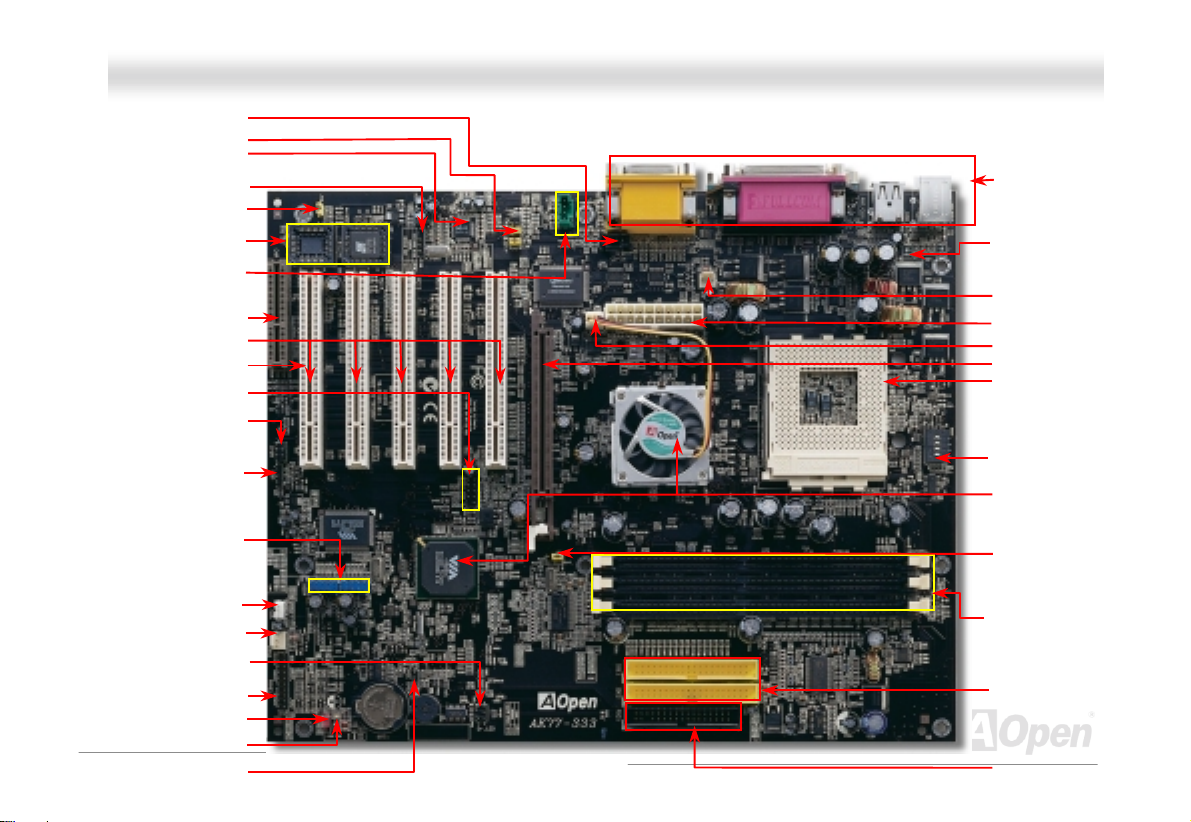
Motherboard Map ..........................................................................................................................................................16
Block Diagram ...............................................................................................................................................................17
Hard war e Ins tal lat ion..................................................................................................................18
Clear CMOS Data ..........................................................................................................................................................19
CPU Installation ............................................................................................................................................................. 20
JP21 FSB/PCI Clock Ratio ............................................................................................................................................22
CPU Jumper-less Design............................................................................................................................................... 23
CPU and Housing Fan Connector (with H/W Monito ring) ...............................................................................................2 8
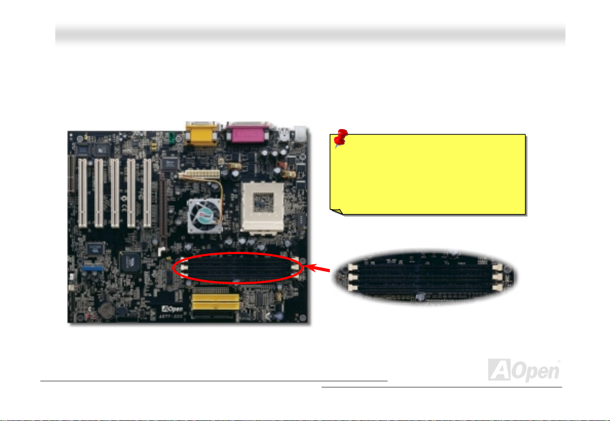
DIMM Sockets ...............................................................................................................................................................29
System and RAM Power Indicate LED ...........................................................................................................................31
Front Panel Connector ..................................................................................................................................................32
2
Page 3

AAKK7777--333333 OOnnlliinnee MMaannuuaall
ATX Power Connector ...................................................................................................................................................33
AC Power Auto Recovery ..............................................................................................................................................34
IDE, Floppy Connector ..................................................................................................................................................35
S/PDIF (Sony/Philips Digital Interface) Connector.........................................................................................................37
Super 5.1 Channel Audio Effect.....................................................................................................................................38
IrDA Connector ..............................................................................................................................................................39
WOM (Zero Voltage Wake on Modem) Connector.........................................................................................................40
WOL (Wake on LAN).....................................................................................................................................................4 3
AGP (Accelerated Graphic Port) Expansion Slot ........................................................................................................... 45
CNR (Communication and Network Riser) Expansi on Slot ............................................................................................46
PC99 Color Coded Back Panel......................................................................................................................................47
Support 2
Support 3rd and 4
Chassis Intrusion Sensor...............................................................................................................................................50
CD Audio Connector......................................................................................................................................................51
AUX-IN Connector.........................................................................................................................................................52
Front Audio Connector...................................................................................................................................................53
Die-Hard BIOS (100% Virus Protection, Upgrad e Optional) ...........................................................................................54
Dr. LED Connector (Upgrade Optional).........................................................................................................................57
nd
USB Port.....................................................................................................................................................48
th
USB2.0 Ports (Optional)..................................................................................................................49
3
Page 4

AAKK7777--333333 OOnnlliinnee MMaannuuaall
Battery-less and Long Life Design.................................................................................................................................59
Over-current Protection .................................................................................................................................................60
Hardware Monitoring .....................................................................................................................................................61
Resettable Fuse ............................................................................................................................................................62
2200μF
Layout (Frequency Isolation Wall) .................................................................................................................................64
Fansink on North Bridge................................................................................................................................................65
Low ESR Capacitor......................................................................................................................................... 63
Driver and Utility..........................................................................................................................66
Auto-run Menu from Bonus CD Disc..............................................................................................................................67
Installing Windows 95....................................................................................................................................................68
Installing Windows 98....................................................................................................................................................69
Installing Windows® 98 SE, Windows® ME & Wi n dow s
Installing VIA 4 in 1 Driver............................................................................................................................................. 7 1
Installing Onboard Sound Driver....................................................................................................................................72
Installing Hardware Monitoring Uti lity ............................................................................................................................73
Installing USB2.0 Driver (Optiona)................................................................................................................................. 74
ACPI Suspend to Hard Drive......................................................................................................................................... 77
ACPI Suspend to RAM (STR)........................................................................................................................................82
®
2000......................................................................................... 70
AWARD BIOS ................................................................................................................................84
4
Page 5

AAKK7777--333333 OOnnlliinnee MMaannuuaall
How To Use Award™ BIOS Setup P rogr am...................................................................................................................85
How To Enter BIOS Set up .............................................................................................................................................87
BIOS Upgrade under Windows environment..................................................................................................................88
Overclocking ................................................................................................................................90
VGA Card & Hard Disk ..................................................................................................................................................91
Glossary .......................................................................................................................................9 2
AC97 .............................................................................................................................................................................92
ACPI (Advanced Configuratio n & Power Interfac e) ........................................................................................................92
AGP (Accelerated Graphic Port)....................................................................................................................................92
AMR (Audio/Modem Riser)............................................................................................................................................93
AOpen Bonus Pack CD .................................................................................................................................................93
APM (Advanced Power Management)........................................................................................................................... 93
ATA (AT Attachment) ...................................................................................................................................................... 93
ATA/66........................................................................................................................................................................... 93
ATA/100 ......................................................................................................................................................................... 94
BIOS (Basic Input/Output Sys tem) ................................................................................................................................ 94
Bus Master IDE (DMA mode).........................................................................................................................................94
CNR (Communication and Networki ng Riser)................................................................................................................94
CODEC (Coding and Decoding) ....................................................................................................................................95
5
Page 6

AAKK7777--333333 OOnnlliinnee MMaannuuaall
DDR (Double Data Rate) SDRAM..................................................................................................................................95
DIMM (Dual In Line Memory Module) ............................................................................................................................95
DMA (Direct Memory Access) ........................................................................................................................................ 95
ECC (Error Checking and Correction)............................................................................................................................96
EDO (Extended Data Output) Memory...........................................................................................................................96
EEPROM (Electronic Erasable Programmab le ROM)....................................................................................................96
EPROM (Erasable Programmabl e ROM).......................................................................................................................96
EV6 Bus ........................................................................................................................................................................97
FCC DoC (Declaration of Conformity)............................................................................................................................ 97
FC-PGA (Flip Chip-Pin Grid Array) ................................................................................................................................97
Flash ROM ....................................................................................................................................................................97
FSB (Front Side Bus) Clock ...........................................................................................................................................9 8
2
I
C Bus ..........................................................................................................................................................................98
IEEE 1394 .....................................................................................................................................................................98
Parity Bit........................................................................................................................................................................99
PBSRAM (Pipelined Burst S RAM) .................................................................................................................................99
PC-100 DIMM ................................................................................................................................................................ 99
PC-133 DIMM ................................................................................................................................................................ 99
PC-1600 or PC-2100 DDR SDRAM.............................................................................................................................100
6
Page 7

AAKK7777--333333 OOnnlliinnee MMaannuuaall
PCI (Peripheral Component Interface) Bus.................................................................................................................. 10 0
PDF Format.................................................................................................................................................................100
PnP (Plug and Play) ....................................................................................................................................................100
POST (Power-On Self Test).........................................................................................................................................101
RDRAM (Rambus DRAM)............................................................................................................................................101
RIMM (Rambus Inline Memory Module)....................................................................................................................... 1 01
SDRAM (Synchronous DRAM) ....................................................................................................................................101
Shadow E
SIMM (Single In Li ne M emory Mod ule)........................................................................................................................ 1 02
SMBus (System Management Bus) .............................................................................................................................102
SPD (Serial Presence Detect ) .....................................................................................................................................102
Ultra DMA .................................................................................................................................................................... 1 03
USB (Universal Serial B us) ..........................................................................................................................................103
VCM (Virtual Channel Memory)................................................................................................................................... 10 4
ZIP file.........................................................................................................................................................................104
2
PROM ........................................................................................................................................................102
Troubleshooting......................................................................................................................... 1 0 5
Technical Support......................................................................................................................10 9
Product Registration..................................................................................................................11 2
How to Conta ct Us.....................................................................................................................113
7
Page 8

AAKK7777--333333 OOnnlliinnee MMaannuuaall
YYoouu MMuusstt NNoottiiccee
Adobe, the Adobe logo, Acrobat is trademarks of Adobe Systems Incorporated.
AMD, the AMD logo, Athlon and Duron are trademarks of Advanced Micro Devices, Inc.
Intel, the Intel logo, Intel Celeron, Pentium II, Pentium III are trademarks of Intel Corporation.
Microsoft, Windows, and Windows logo are either registered trademarks or trademarks of Microsoft Corporation in the United
States and/or other countries.
All product and brand names used on this manual are used for identification purposes only and may be the registered
trademarks of their respective owners.
All of the specifications and information contained in this manual are subject to change without notice. AOpen reserves the right
to revise this publication and to make reasonable changes. AOpen assumes no responsibility for any errors or inaccuracies that
may appear in this manual, including the products and software described in it.
This documentation is protected by copyright law. All rights are reserved.
No part of this document may be used or reproduced in any form or by any means, or stored in a database or retrieval
system without prior written permission from AOpen Corporation.
Copyright
©
1996-2000, AOpen Inc. All Rights Reserved.
8
Page 9

AAKK7777--333333 OOnnlliinnee MMaannuuaall
BBeeffoorree YYoouu SSttaarrtt
This Online Manual will introduce to the user how this product is installed. All useful information will be described in later
chapters. Please keep this manual carefully for future upgrades or system configuration changes. This Online Manual is saved
in PDF format
get free download from Adobe web site
Although this Online Manual is optimized for screen viewing, it is still capable for hardcopy printing, you can print it by A4 paper
size and set 2 pages per A4 sheet on your printer. To do so, choose File > Page Setup and follow the instruction of your printer
driver.
Thanks for the help of saving our earth.
, we recommend using Adobe Acrobat Reader 4.0 for online viewing, it is included in Bonus CD disc or you can
.
9
Page 10

AAKK7777--333333 OOnnlliinnee MMaannuuaall
OOvveerrvviieeww
Thank you for choosing AOpen AK77-333. The AK77-333 is AMD® Socket 462 motherboard (M/B) based on the ATX form factor
featuring the VIA Apollo KT333 chipset
Athlon™ & Duron™ processor and 200/266MHz EV6
AGP /4X mode and pipelined spilt-transaction long burst transfer up to 1056MB/sec. With high bandwidth 200/266MB/s 8-bit
V-Link Host Controller, DDR266(PC2100)
maximum memory size can be up to 3GB. The on-board IDE controller supports Ultra DMA
rate up to 133MB/s. Further flexibility can be
achieved by taking advantage of the
Communication and Network Riser (CNR)
option that allows audio and modem configuration
on a single baseboard design. Besides, the
AK77-333 has an AC97
chipset onboard for provides high performance and
magic surround stereo sound to let people enjoy
working with it. More than that, this motherboard
supports USB 2.0 function (USB3 and USB4 only,
optional) with a fancy speed up to 480Mbps. Now,
enjoy all features from AOpen AK77-333.
. As high performance chipset built in the M/B, the AK77-333 AMD® Socket 462 series
system bus. In the AGP performance, it has one AGP slot and supports
and DDR333(PC2700) DDR SDRAM can be applied to the AK77-333 and the
66/100/133 mode and the transfer
card
CODEC Realtek ALC650
10
Page 11

AAKK7777--333333 OOnnlliinnee MMaannuuaall
FFeeaattuurree HHiigghhlliigghhtt
CPU
Supports AMD® Socket 462 series CPU with both 200MHz and 266MHz EV6 Bus designed for Socket 462 technology.
Athlon: 600MHz~1.4GHz
Duron: 600MHz~1.2GHz
AthlonXP: 1500+(1.3GHz)~2000+(1.667GHz)
Chipset
The VIA Apollo KT333 consists of the KT333 V-Link DDR Host system controller and the VT8233A highly integrated V-Link
Client PCI/LPC controller. The Host system controller provides superior performance between the CPU, SDRAM, AGP bus, and
V-Link interface with pipelined, burst, and concurrent operation. The VT8233A V-Link Client controller is a highly integrated
PCI/LPC controller. Its internal bus structure is based on 66MHz PCI bus that provides 2x bandwidth compare to previous
generation PCI/ISA bridge chips. The VT8233A integrated Client V-Link controller with 200/266MB/s bandwidth between
Host/Client V-Link interface, provides a V-Link-PCI and V-Link-LPC controller. Of five PCI slots provided, AK77-333 supports all
five master PCI slots with arbitration and decoding for all integrated functions and LPC bus.
Ultra DMA 66/100/133 Bus Master IDE
Comes with an on-board PCI Bus Master IDE controller with two connectors that supports four IDE devices in two channels,
supports Ultra DMA
66/100/133, PIO Modes 3 and 4 and Bus Master IDE DMA Mode 4, and supports Enhanced IDE devices.
11
Page 12

AAKK7777--333333 OOnnlliinnee MMaannuuaall
Expansion Slots
Including five 32-bit/33MHz PCI, one CNR and one AGP 4X slots. The PCI local bus throughput can be up to 132MB/s. The
Communication & Nectworking Riser (CNR)
The Accelerated Graphics Port (AGP)
video cards support data transfer rate up to 1056MB/s. As AK77-333 includes one AGP expansion slot for a bus mastering AGP
graphic card, For AD and SBA signaling, AK77-333 can support 133MHz 2X/4X mode. Of five PCI slots provided, AK77-333
supports four master PCI sl ots for arbi trat ion and decodi ng func tions and one s lave PCI slot .
slot provided from AK77-333 can support CNR interface for a Modem/Audio card.
specification provides a new level of video display sophistication and speed. The AGP
Memory
With VIA Apollo KT333 chipset, the AK77-333 can support Double-Data-Rate (DDR) SDRAM. The DDR S DRAM i nte rfac e all ows
zero wait state bursting between the SDRAM and the data buffers at 266/333MHz. The six banks of DDR SDRAM can be
composed of an arbitrary mixture of 1M/2M4M/8M/16M/32M/64MxN DDR SDRAM and maximum up to 3GB. The AK77-333
allows DDR SDRAM to run at either synchronous or pseudo-synchronous mode with the host CPU bus frequency
(266/333MHz).
On-board AC97 Sound
AK77-333 uses the AC97 CODEC Realtek ALC650 chip, which supports high quality of 5.1 Channel audio effects. This on-board
audio includes a complet e audio rec ording and playbac k s yst em .
12
Page 13

AAKK7777--333333 OOnnlliinnee MMaannuuaall
Eight USB Connectors (3rd and 4th connector are USB2.0, optional)
Provides four ports, eight USB connectors for USB interface devices, such as mouse, keyboard, modem, scanner, etc. The
onboard 1
power mode and wake-up specification. While, the 3
which is 40 times faster than the traditional one
st
and 2nd USB Host controller are fully compliant with USB UHCI 1.1 specification that can fully compatible with low
rd
and 4th connector support USB2.0 have a fancy speed up to 480Mbps
1MHz Stepping Frequency Adjustment
Provides “1MHz Stepping Frequency Adjustment” function in the BIOS. This magic function allows you adjust CPU FSB
frequency from 100~248 by 1MHz stepping, and lets your system can get maximum performance.
Watch Dog Timer
Includes AOpen “Watch Dog Timer” function that can auto-reset system in 4.8 seconds when you fail to system overclocking.
Die-Hard BIOS with external controller (Upgrade Optional)
The Die-Hard BIOS technology is a very effective hardware protection method that doesn’t involve any software or BIOS coding.
Hence, it is 100% virus free.
Dr. LED (Upgrade Optional)
The Dr. LED has 8 LEDs on AK77-333, which can easily show what kind of problem you may encounter.
13
Page 14

AAKK7777--333333 OOnnlliinnee MMaannuuaall
Power Management/Plug and Play
The AK77-333 supports the power management function that confirms to the power-saving standards of the U.S. Environmental
Protection Agency (EPA) Energy Star program. It also offers Plug-and-Play
problems, thus making the system much more user-friendly.
, which helps saving users from configuration
Hardware Monitoring Management
Supports CPU or system fans status, temperature and voltage monitoring and alert, through the on-board hardware monitor
module and Aopen Hardware Monitoring Utility
.
Enhanced ACPI
Fully implement the ACPI standard for Windows® 95/98/ME/NT/2000 series compatibility, and supports Soft-Off, STR (Suspend
to RAM, S3), STD (Suspend to Disk, S4), WOM (Wake On Modem), WOL (Wake On LAN) features.
Super Multi-I/O
The AK77-333 provides two high-speed UART compatible serial ports and one parallel port with EPP and ECP capabilities.
UART2 can also be directed from COM2 to the Infrared Module for the wireless connections.
14
Page 15

AAKK7777--333333 OOnnlliinnee MMaannuuaall
QQuuiicckk IInnssttaallllaattiioonn PPrroocceedduurree
This page gives you a quick procedure on how to install your system. Follow each step accordingly.
1. Installing CPU and Fan
2. Installing System Memory (DIMM)
3. Connecting Front Panel Cable
4. Connecting IDE and Floppy Cable
5. Connecting ATX Power Cable
6. Connecting Back Panel Cable
7. Power-on and Load BIOS Setup Default
8. Setting CPU Frequency
9. Reboot
10. Insta lli ng O pe rat in g Sys tem (s uch as W ind ows 98 )
11. Installing Driver and Utility
15
Page 16
A
A
A
A
(
r
r
r
r
r
r
r
r
r
d
(Op
)
r
AAKK7777--333333 OOnnlliinnee MMaannuuaall
CD-IN Connector
Front Audio Connector
Onboard AC97 CODEC
Realtek ALC650
S/PDIF Connecto
JP30 Die Hard BIOS
Select Jumper
Die Hard BIOS with 100% Virus
Protection (Upgrade Optional)
Green: AUX-IN Connecto
CNR Expansion Slot
32-bit PCI Expansion Slot x5
2nd USB V1.1 Port Connector
JP14 CMOS Data Clear Jumper
(PCI 5 supports slave mode
PCI card only)
IrDA Connecto
WOM (Wake ON Modem)
r
3
and 4th USB V2.0 Port
WOL (Wake ON LAN)
FAN3 Connecto
with H/W Monitoring
Front Panel Connecto
Connecto
Connector
Dr. LED Connecto
(Upgrade Optional)
System & RAM Power
Indicate LED
Chassis Intrusion Senso
tional
Connecto
Connecto
Motherboard Map
16
PC99 Colored Back Panel
Resetable Fuse
CPU Fan Connector with
H/W Monitoring
TX Power Connector
FAN3 Connector
GP 4x Expansion Slot
462-pin CPU Socket with
Voltage and Frequency
uto-Detection that supports
MDTM AthlonTM / DuronTM /
TM
and Athlon
SW1 CPU Ratio Select Switch
VIA® Apollo KT333
Chipset with FANsink and
VT8233A SB
ATA100/133 supported)
JP21 FSB Select Jumper
184-pin DIMMx3 supports
DDR333/DDR266
(Max. to 3B)
IDE Connector x 2
(ATA/66/100/133 supported)
FDD Connector
XP
Page 17
AAKK7777--333333 OOnnlliinnee MMaannuuaall
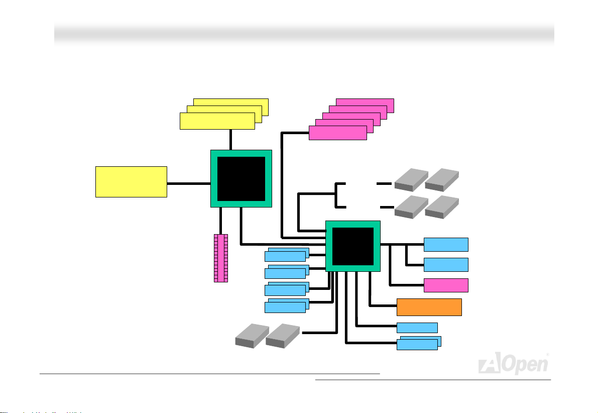
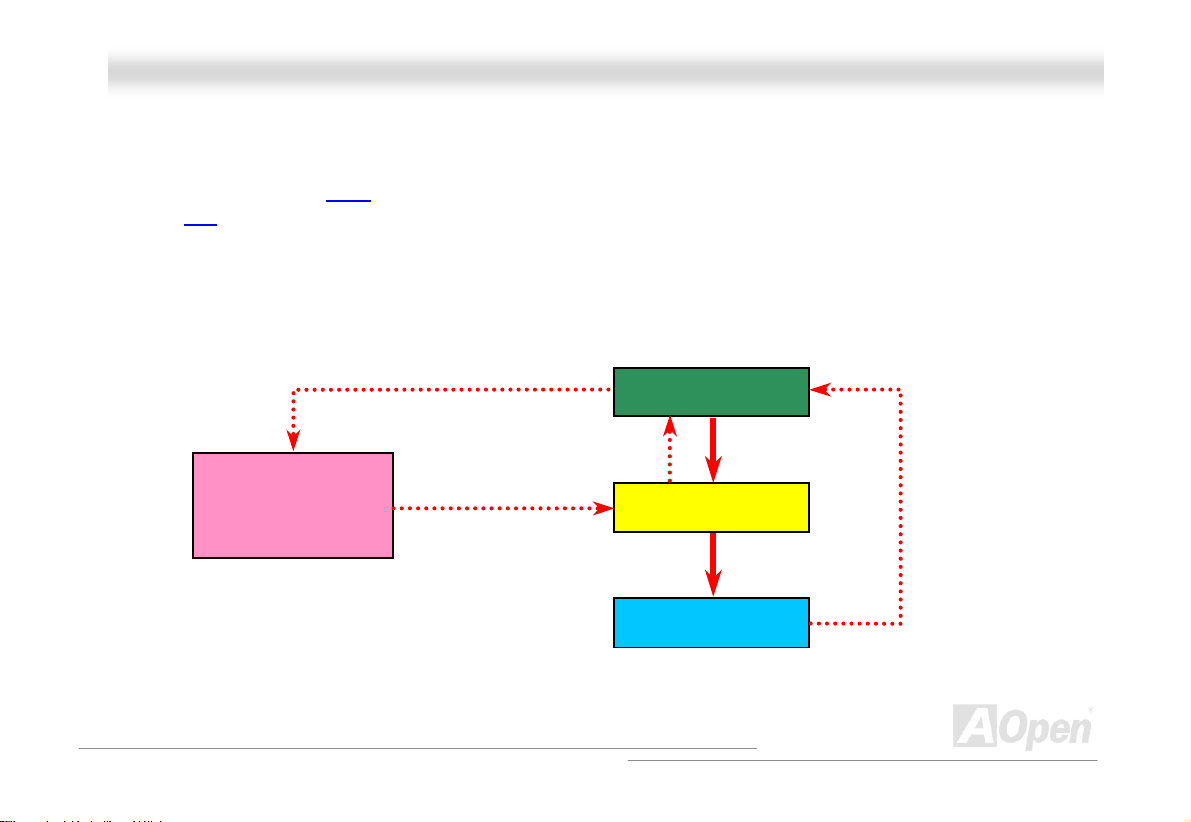
BBlloocckk DDiiaaggrraamm
Socket 462
AMD
Athlon/D uron
CPU
100/133MHz
System Bus
PC2100/PC2700 DDR
SDRAM Up to 3GB
DDR SDRAM Socket x3
VIA KT333
AGP Bus
AGP 4X Slot
Floppy Disk Drive x2
PCI Bus
1stUSB Port
2ndUSB Port
3rdUSB Port
4thUSB Port
USB connector x8
32-bit P CI Slot x5
ATA
66/100/133
Primary
Channel
Secondar y
Channel
VT8233A
IDE Dri ve x4
AC’97 Link
Audio CODEC
Modem CODEC
CNR Slot
2MBit Flash EEPROM
Parallel Port
Serial Port x2
17
Page 18

AAKK7777--333333 OOnnlliinnee MMaannuuaall
HHaarrddwwaarree IInnssttaallllaattiioonn
This chapter describes jumpers, connectors and hardware devices of this motherboard.
Note: E lectrostatic discharge (ESD) can damage your processor, disk drives, expansion boards,
and other components. Always observe the following precautions before you install a system
component.
1. Do not remove a component from its protective packaging until you are ready to install it.
2. Wear a wrist ground strap and attach it to a metal part of the system unit before handling a
component. If a wrist strap is not available, maintain contact with the system unit throughout
any procedures requiring ESD protection.
18
Page 19
AAKK7777--333333 OOnnlliinnee MMaannuuaall
Pin 1
1
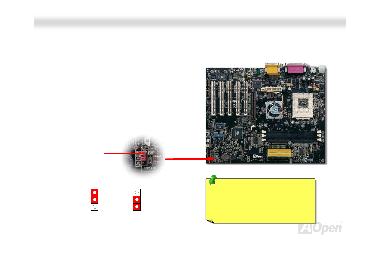
Clear CMOS
Tip: W hen should I Clear CMOS?
1. Boot fa il bec aus e of ove rc lock i ng…
2. Forget password…
3. Troubleshooting…
CClleeaarr CCMMOOSS DDaattaa
You can clear CMOS to restore system default setting. To clear the CMOS, follow the procedures below.
1. Turn off the system and unplug the AC power.
2. Remove ATX power cable from connector PWR2.
3. Locate JP14 and short pins 2-3 for a few seconds.
4. Return JP14 to its normal setting by shorting pin 1 & pin 2.
5. Connect ATX power cable back to connector PWR2.
1
Normal Operation
(default)
19
Page 20
AAKK7777--333333 OOnnlliinnee MMaannuuaall
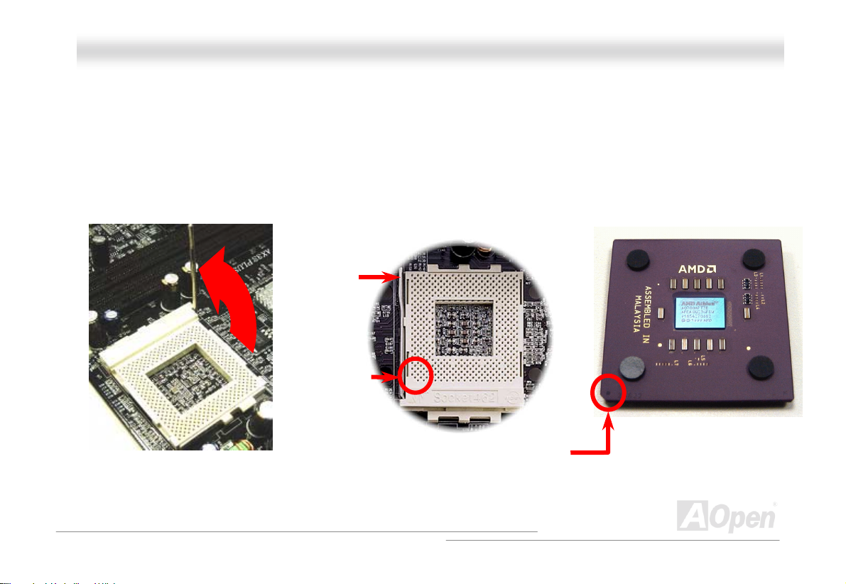
CCPPUU IInnssttaallllaattiioonn
This motherboard supports AMD® Athlon and Duron Socket 462 series CPU. Be careful of CPU orientation when you plug it into
CPU socket.
1. Pull up the CPU socket lever and
up to 90-degree angle.
2. Locate Pin 1 in the socket and look for a black dot or cut edge on the
CPU upper interface. Match Pin 1 and cut edge, then insert the CPU into
the socket.
CPU socket
Lever
Note: This picture is for example only, it may not exactly be the same motherboard.
CPU pin 1
and cut edge
Black dot
and cut edge
20
Page 21
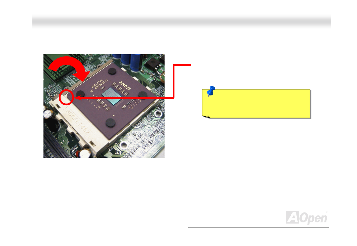
y
AAKK7777--333333 OOnnlliinnee MMaannuuaall
3. Press down the CPU socket lever and finish
CPU installation.
Note: This picture is for example only, it may not exactly be the same motherboard.
CPU cut edge
Note: If you do not match the CPU
socket Pin 1 and CPU cut edge well, it
ma
damage the CPU.
21
Page 22
(
AAKK7777--333333 OOnnlliinnee MMaannuuaall
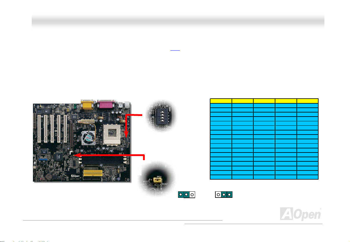
JJPP2211 FFSSBB//PPCCII CClloocckk RRaattiioo
This jumper is used to specify the relationship of PCI and FSB clock. Generally speaking, if you are not overclockers, we
recommend you to set it to the default setting. Additionally, this motherboard also provides “1MHz Stepping Adjustment”
feature for overclockers to adjust CPU FSB frequency via BIOS setup program. Based on the CPU type, the adjustment range
has two levels: 100~129 (FSB=100, such as Athlon 800), 130~248 (FSB=133, such as Athlon 1000) MHz for your choosing. You
may also choose a specific FSB frequency ranging from 100~117 (say, 105, 110, 115 for example) and 120~156 with reference
to a frequency table in BIOS setup program. If you fix t he CPU FSB frequency by JP21, the “1MHz Stepping Adjustment” range
will be changed and following your JP21 setting.
-
SW1 CPU Ratio
Select Switch
+
1
2
3
4
1 2 3
FSB=100
CPU Ratio SW1-1 SW1-2 SW1-3 SW1-4
5
5.5
6
6.5
7
7.5
8
8.5
9
9.5
10
10.5
11
11.5
12
12.5
CPU Default 0 0 0 0
--+-
+-+-
-++-
+++-
---+
+--+
-+-+
++-+
--++
+-++
-+++
++++
----
+---
-+--
++--
FSB=133
Default)
22
Page 23
AAKK7777--333333 OOnnlliinnee MMaannuuaall
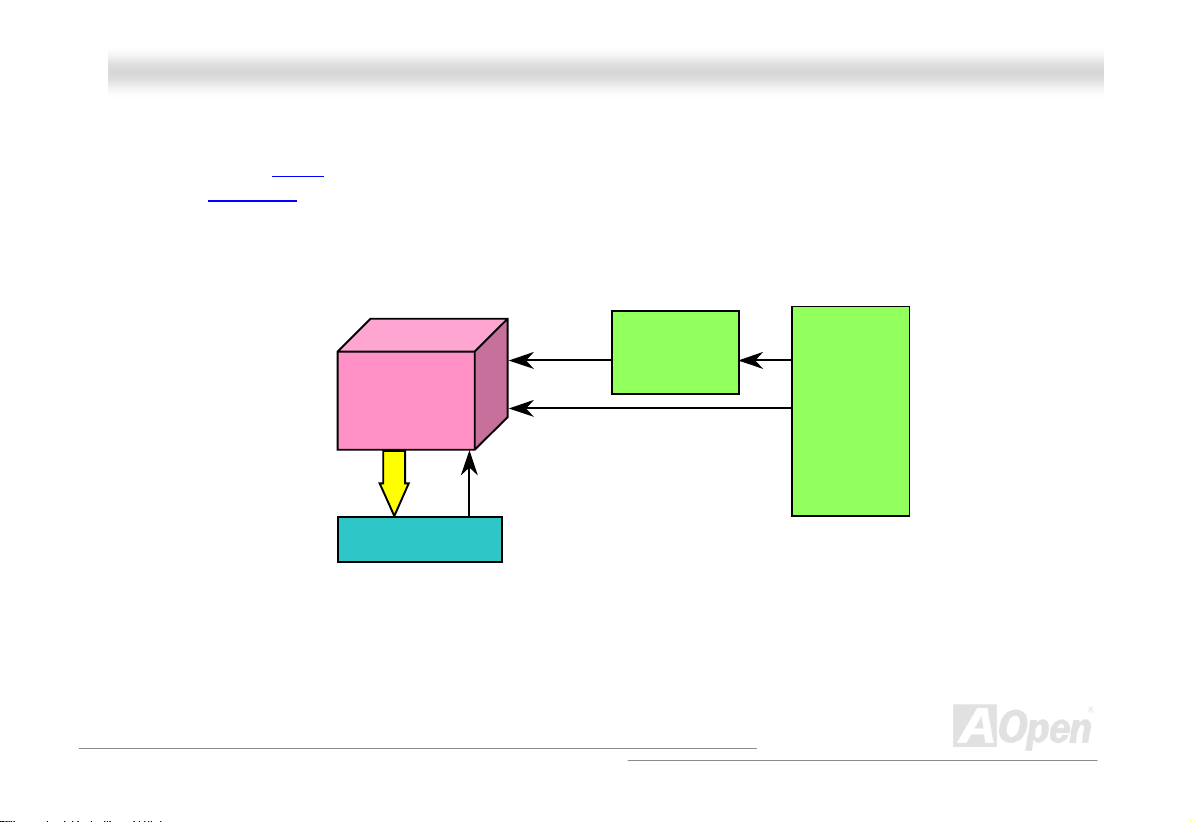
CCPPUU JJuummppeerr--lleessss DDeessiiggnn
CPU VID signal and SMbus clock generator provide CPU voltage auto-detection and allows the user to set the CPU frequency
through the BIOS setup
designs are eliminated. There will be no worry of wrong CPU voltage detection.
, therefore no jumpers or switches are used. The disadvantages of the Pentium based jumper-less
AMD
Socket A CPU
CPU VID signal
Power Regulator
(A utomatically generates CPU voltage)
CPU Freq. Ratio
CPU voltage
Clock
Generator
BIOS
Controlled
Circuit
23
Page 24
AAKK7777--333333 OOnnlliinnee MMaannuuaall
FFuullll--rraannggee AAddjjuussttaabbllee CCPPUU CCoorree VVoollttaaggee
This function is dedicated to overclockers, AOpen works together with Fairchild t o develop a special chip FM3540 that s upports
Adjustable CPU Core Voltage from 1.1V to 1.85V by 0.05V stepping. But this motherboard can also automatically detect CPU
VID signal and generates proper CPU core voltage.
BIOS Setup > Frequency/Voltage Control > CPU Voltage Setting
Warning: Higher CPU core voltage may be
able to increase CPU speed for overclocking,
but you may damage the CPU or reduce the
CPU lifecycle.
24
Page 25
AAKK7777--333333 OOnnlliinnee MMaannuuaall
SSeettttiinngg CCPPUU FFrreeqquueennccy
This motherboard is CPU jumper-less design, you can set CPU frequency through the BIOS setup, and no jumpers or switches
are needed.
BIOS Setup > Frequency/Voltage Control > CPU Speed Setting
CPU Ratio
CPU FSB
(By BIOS Table)
CPU FS B
(By manual Adjustment)
From 5.5x to 12.5x step 0.5x
100, 102, 105, 108, 110, 113, 115, 117, 120, 122, 124, 133, 136,
138, 140, 142, 144, 147, 152, 154, and 156MHz.
FSB=100, 100~129 by 1MHz stepping adjustment technology
FSB=133, 130~248 by 1MHz stepping adjustment technology
Home
y
Warning: VIA® Apollo KT333 chipset supports 133MHz
FSB (with performance reaches maximum 266MHz EV6
system bus) and 66MHz AGP clock, higher clock setting
may cause serious system damage.
Tip: If your system hangs or fails to boot because of
overclocking, simply use <Home> key to restore the
default setting or you can wait the AOpen “Watch Dog
Timer” reset the system after five seconds and system
will auto-detect hardware again.
25
Page 26
AAKK7777--333333 OOnnlliinnee MMaannuuaall
SSuuppppoorrtteedd CCPPUU FFrreeqquueennccyy
Core Frequency = CPU Bus Clock * CPU Ratio
PCI Clock = CPU Bus Clock / Clock Ratio
AGP Clock = PCI Clock x 2
EV6 Bus Speed = CPU external bus clock x 2
CPU CPU Core Frequency EV6 Bus Clo ck Ratio
Athlon 1G 1GHz 200MHz 10.0x
Athlon 1.1G 1.1GHz 200MHz 11.0x
Athlon 1.2G 1.2GHz 200MHz 12.0x
Athlon 1.3G 1.3GHz 200MHz 13.0x
Athlon 1G 1GHz 266MHz 7.5x
Athlon 1.13G 1.13GHz 266MHz 8.5x
Athlon 1.2G 1.2GHz 266MHz 9.0x
Athlon 1.33G 1.33GHz 266MHz 10.0x
Athlon 1.4G 1.4GHz 266MHz 10.5x
AthlonXP 1500+ 1.3GH z 266MHz 10.0x
AthlonXP 1600+ 1.4GH z 266MHz 10.5x
AthlonXP 1700+ 1.46GHz 266MHz 11.0x
AthlonXP 1800+ 1.53GHz 266MHz 11.5x
AthlonXP 1900+ 1.6GH z 266MHz 12.0x
Duron 800 800MHz 200MHz 8.0x
Duron 850 850MHz 200MHz 8.5x
Duron 900 900MHz 200MHz 9.0x
Duron 950 950MHz 200MHz 9.5x
Duron 1G 1GHz 200MHz 10.0x
Duron 1.1G 1.1GHz 200MHz 11.0x
Note: This motherboard support
CPU auto-detection function.
Hence, you don’t need to setup
the CPU frequency manually.
26
Page 27
AAKK7777--333333 OOnnlliinnee MMaannuuaall
AAOOppeenn ““WWaattcchh DDoogg TTiimmeerr””
With this motherboard, AOpen provides a very special, useful feature for overclockers. When you power-on the system, the
BIOS will check last system POST
the CPU FSB
reset the system to reboot in five seconds. Then, BIOS will detect the CPU’s default frequency and POST again. With this
special feature, you can easily overclock your system to get higher system performance without removing the cover of system
housing, and be able to set the jumper to clear CMOS data when your system hanged.
frequency by user’s setting that stored in the BIOS. If system failed in BIOS POST, the “Watch Dog Timer” will
AOpen
Watch Dog
Timer
status. If it succeeded, the BIOS will enable “Watch Dog Timer” function immediately, and set
Enable/Disable Signal
from BIOS
Countdown about
5 seconds if fails
in POST
Reset Signal
Clock Generator
BIOS
CPU ID Signal
CPU
27
Page 28
AAKK7777--333333 OOnnlliinnee MMaannuuaall
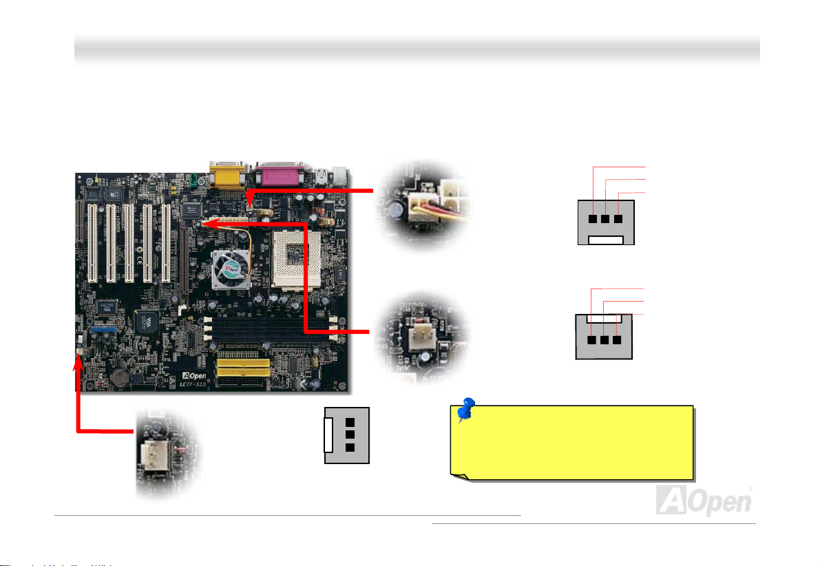
CCPPUU aanndd HHoouussiinngg FFaann CCoonnnneeccttoorr ((wwiitthh HH//WW MMoonniittoorriinngg))
Plug in the CPU fan cable to the 3-pin CPU FAN connector. If you have chassis fan, you can also plug it on System Fan (FAN2)
or AUX Fan (FAN3) (without H/W monitoring) connector.
FAN2 Connector
GND
+12V
SENSOR
FAN3 Connector
CPU Fan Connector
Note: Some CPU fans do not have
sensor pin, so that cannot support fan
monitoring.
GND
+12V
SENSOR
SENSOR
+12V
GND
28
Page 29
AAKK7777--333333 OOnnlliinnee MMaannuuaall
DDIIMMMM SSoocckkeettss
This motherboard has three 184-pin DDR DIMM sockets that allow you to install PC2100 or PC2700 memory up to 3 GB. Only
Non-ECC DDR SDRAM are supported.
Warning: The AK77-333 support DDR
SDRAM, p lease do no t install the SDRAM
on the DDR SDRAM sockets. Otherwise, it
will cause serious damage on memory
sockets or SDRAM module.
DDR
SDRAM
29
Page 30
AAKK7777--333333 OOnnlliinnee MMaannuuaall
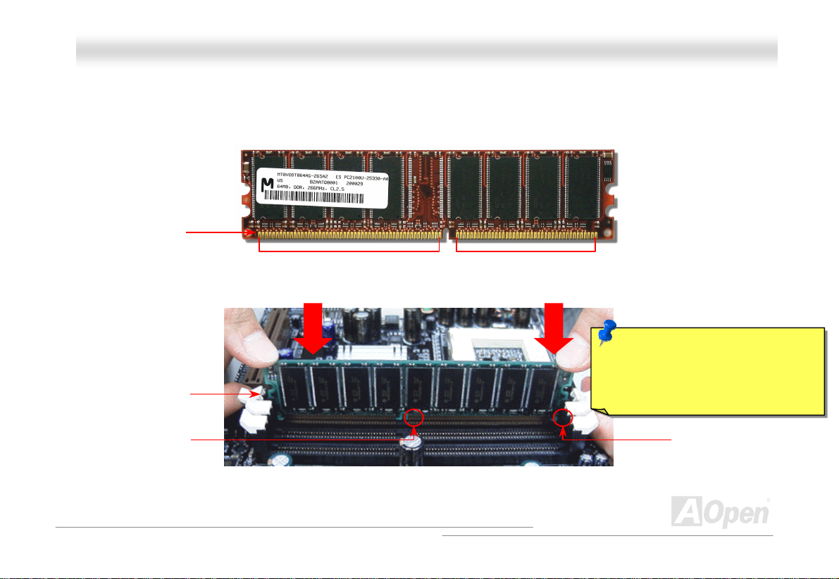
HHooww ttoo IInnssttaallll MMeemmoorryy MMoodduulleess
Please follow the procedure as shown below to finish memory installation.
1. Make sure the DIMM module’s pin face down and match the socket’s size as depicted below.
2. Insert the module straight down to the DIMM slot with both hands and press down firmly until the DIMM module is securely
in place.
3. Repeat step 2 to finish additional DIMM modules installation.
Pin 1
Tab
Key
52 pins 40 pins
Note: The tabs of the DIMM slot will
close- up to hold the DIMM i n place
when the DIMM touches the slot’s
bottom.
Pin 1
30
Page 31

AAKK7777--333333 OOnnlliinnee MMaannuuaall
SSyysstteemm aanndd RRAAMM PPoowweerr IInnddiiccaattee LLEEDD
This LED indicates there is power applies to motherboard and memory. If you connect power to the motherboard, this LED will
be lighting. It is useful to check the system power status when power on/off and stand-by mode or RAM power status during
Suspend to RAM mode
Warning: Do not install or remove the DIMM module or others
devices when the LED is lighting.
.
System
Power LED
31
Page 32

e
A
A
A
AAKK7777--333333 OOnnlliinnee MMaannuuaall
FFrroonntt PPaanneell CCoonnnneeccttoorr
IDE LED
SPEAKER
Attach the power LED, EMPI, speaker, power and reset switch connectors to th
corresponding pins. If you enable “Suspend Mode” item in BIOS Setup, the ACPI
& Power LED will keep flashing while the system is in suspend mode.
Locate the power switch cable from your ATX housing. It is 2-pin female
connector from the housing front panel. Plug this connector to the soft-power
switch connector marked SPWR.
Suspend Type ACPI L E D
Power on Suspend (S1) Flashing for every second
Suspend to RAM (S3) or Suspend to Disk (S4) The LED will be turned off
1
Power Switch
CPI & Power LED
RESET
IDE LED
IDE LED
SPEAKER
NC
NC
+5V
+5V
+5V
GND
NC
1
SPWR
GND
CPILED-
GND
CPILED+
NC
NC
GND
RESET
GND
32
Page 33

AAKK7777--333333 OOnnlliinnee MMaannuuaall
AATTXX PPoowweerr CCoonnnneeccttoorr
The ATX power supply uses 20-pin connector shown below. Make sure you plug in the right direction.
COM
+5V
COM
+3.3V
+3.3V
+3.3V
-12V
COM
PS-ON
COM
+5V
COM
PW-OK
5VSB
+12V
+5V
+5V
-5V
COM
COM
33
Page 34

AAKK7777--333333 OOnnlliinnee MMaannuuaall
AACC PPoowweerr AAuuttoo RReeccoovveerryy
A traditional ATX system should remain at power off stage when AC power resumes from power failure. This design is
inconvenient for a network server or workstation, without an UPS, that needs to keep power-on. This motherboard implements
an AC Power Auto Recovery function to solve this problem.
34
Page 35

A
AAKK7777--333333 OOnnlliinnee MMaannuuaall
IIDDEE,, FFllooppppyy CCoonnnneeccttoorr
Connect 34-pin floppy cable and 40-pin IDE cable to floppy connector FDC connector. Be careful of the pin1 orientation. Wrong
orientation may cause system damage.
Primary
Slave (2nd)
Pin 1
Secondary
Slave (4th)
Pin 1
Primary
Master (1st)
IDE1 (Primary)
IDE2 (Secondary)
TA 66/100/133
IDE Connector
Secondary
Master (3rd)
FDD
Connector
35
Page 36

AAKK7777--333333 OOnnlliinnee MMaannuuaall
IDE1 is also known as the primary channel and IDE2 as the secondary channel. Each channel supports two IDE devices that
make a total of four devices. In order to work together, the two devices on each channel must be set differently to Master and
Slave mode. Either one can be the hard disk or the CDROM. The setting as master or slave mode depends on the jumper on
your IDE device, so please refer to your hard disk and CDROM manual accordingly.
This motherboard supports ATA66
modes. The IDE bus is 16-bit, which means every transfer is two bytes.
Mode Clock Period Clock Count Cycle TimeData Transfer Rate
PIO mode 0 30ns 20 600ns (1/600ns) x 2byte = 3.3MB/s
PIO mode 1 30ns 13 383ns (1/383ns) x 2byte = 5.2MB/s
PIO mode 2 30ns 8 240ns (1/240ns) x 2byte = 8.3MB/s
PIO mode 3 30ns 6 180ns (1/180ns) x 2byte = 11.1MB/s
PIO mode 4 30ns 4 120ns (1/120ns) x 2byte = 16.6MB/s
DMA mode 0 30ns 16 480ns (1/480ns) x 2byte = 4.16MB/s
DMA mode 1 30ns 5 150ns (1/150ns) x 2byte = 13.3MB/s
DMA mode 2 30ns 4 120ns (1/120ns) x 2byte = 16.6MB/s
ATA33 30ns 4 120ns (1/120ns) x 2byte x 2 = 33MB/s
ATA66 30ns 2 60ns (1/60ns) x 2byte x 2 = 66MB/s
ATA100 20ns 2 40ns (1/40ns) x 2byte x 2 = 100MB/s
ATA133 15ns 2 30ns (1/30ns) x 2byte x 2 = 133MB/s
Warning: Th e sp ec ific at io n of the I DE c abl e is a max imu m of 46c m (1 8 inc hes ) ;
make sure your cable does not exceed this length.
, ATA100 or ATA133 DE devices. Following table lists the transfer rate of IDE PIO and DMA
Tip:
1. For better signal quality,
it is recommended to set
the far end side device
to master mode and
follow the suggested
sequence to install your
new device. Please refer
to above diagram
2. To achieve the best
performance of Ultra
DMA 66/100 hard disks,
a special 80-wires IDE
cable for Ultra DMA
1 i r
ir
.
36
Page 37

A
AAKK7777--333333 OOnnlliinnee MMaannuuaall
SS//PPDDIIFF ((SSoonnyy//PPhhiilliippss DDiiggiittaall IInntteerrffaaccee)) CCoonnnneeccttoorr
S/PDIF (Sony/Philips Digital Interface) is a newest audio transfer file format, which provides impressive quality through optical
fiber and allows you to enjoy digital audio instead of analog audio. Normally there are two S/PDIF outputs as shown, one for
RCA connector, the most common one used for consumer audio products, and the other for optical connector with better audio
quality. Through a specific audio cable, you can connect the S/PDIF connector to other end of the S/PDIF audio module, which
bears S/PDIF digital output. However, you must have a S/PDIF supported speaker with S/PDIF digital input to connect to the
S/PDIF digital output to make the most out of this function.
Connecting to
Connecting to
Optical Cable
S/PDIF Module
udio cable
37
Page 38

AAKK7777--333333 OOnnlliinnee MMaannuuaall
SSuuppeerr 55..11 CChhaannnneell AAuuddiioo EEffffeecctt
This motherboard comes with an ALC650 Codec which supports high quality of 5.1 Channel audio effect, bringing you a brand
new audio experience. On the strength of the innovative design of ALC650, you're able to use standard line-jacks for surround
audio output without connecting any external module. To apply this function, you have to install the audio driver in the Bonus
Pack CD as well as an audio application supporting 5.1 Channel. Picture bellow represents the standard location of all speakers
in 5.1 Channel sound track. Please connect the plug of your front speakers to the green “Speaker out” port, rear speakers’ plug
to the blue “Line in” port and both of the center and subwoofer speakers to the red “MIC in” port.
38
Page 39

X
AAKK7777--333333 OOnnlliinnee MMaannuuaall
IIrrDDAA CCoonnnneeccttoorr
The IrDA connector can be configured to support wireless infrared module, with this module and application software such as
Laplink or Windows 95 Direct Cable Connection, the user can transfer files to or from laptops, notebooks, PDA devices and
printers. This connector supports HPSIR (115.2Kbps, 2 meters) and ASK-IR (56Kbps).
Install the infrared module onto the IrDA connector and enable the infrared function from BIOS Setup, UART2 Mode
to have the correct orientation when you plug in the IrDA connector.
Pin 1
IR_T
IrDA Connector
NC
+5V
, make sure
KEY
GND
IR_RX
39
Page 40

AAKK7777--333333 OOnnlliinnee MMaannuuaall
WWOOMM ((ZZeerroo VVoollttaaggee WWaakkee oonn MMooddeemm)) CCoonnnneeccttoorr
This motherboard implements special circuit to support Wake On Modem, both Internal modem card and external box modem
are supported. Since Internal modem card consumes no power when system power is off, it is recommended to use an internal
modem. To use internal modem, connect 4-pin cable from RING connector of modem card to the WOM connector on the
motherboard.
WOM Connector
+5VSB
NC
RI-
GND
40
Page 41

AAKK7777--333333 OOnnlliinnee MMaannuuaall
WWOOMM bbyy EExxtteerrnnaall BBOOXX MMooddeem
Traditional Green PC suspend mode does not really turn off the system power supply, it uses external box modem to trigger MB
COM port and resume back to active.
Note: This picture is for example only, it may not exactly be the same motherboard.
Pin 1
Pin 1
m
Serial Port
(Modem Side)
Serial Port
(Motherboard Side)
41
Page 42

AAKK7777--333333 OOnnlliinnee MMaannuuaall
WWOOMM bbyy IInntteerrnnaall MMooddeemm CCaarrd
With the help of the ATX soft power On/Off, it is possible to have a system totally power off, and wakeup to automatically answer
a phone call as an answering machine or to send/receive a fax. You may identify whether or not your system is in true power off
mode by checking to see if the fan of your power supply is off. Both an external box modem and an internal modem card can be
used to support Modem Wake Up, but if you use an external modem, you have to leave your box modem on.
WOM Connector
(Motherboard Side)
Note: This picture is for example only, it may not exactly be the same motherboard.
d
42
WOM Connector
(Modem Card
Page 43

AAKK7777--333333 OOnnlliinnee MMaannuuaall
WWOOLL ((WWaakkee oonn LLAANN))
This feature is very similar as Wake On Modem, but it goes through local area network. To use Wake On LAN function, you must
have a network card with chipset that supports this feature, and connect a cable from LAN card to motherboard W OL connector.
The system identification information (probably IP address) is stored on network card and because there is a lot of traffic on the
Ethernet, you need to install network management software, such as ADM, for the checking of how to wake up the system. Note
that, at least 600mA ATX standby current is required to support the LAN card for this function.
LID
GND
+5VSB
43
Page 44

AAKK7777--333333 OOnnlliinnee MMaannuuaall
WOL Connector
(Motherboard Side)
Note: This picture is for example only, it may not exactly be the same motherboard.
WOL Connector
(Ethernet Card Side)
44
Page 45

AAKK7777--333333 OOnnlliinnee MMaannuuaall
AAGGPP ((AAcccceelleerraatteedd GGrraapphhiicc PPoorrtt)) EExxppaannssiioonn SSlloott
The AK77-333 provides an AGP 2x4x slot. The AGP 2x4x is a bus interface targeted for high-performance 3D graphic. AGP
supports only memory read/write operation and single-master single-slave one-to-one only. AGP uses both rising and falling
edge of the 66MHz clock, for 2X AGP, the data transfer rate is 66MHz x 4byt es x 2 = 528MB/s. AGP is now moving to AGP 4x
mode, 66MHz x 4bytes x 4 = 1056MB/s. This AGP expansion slot is for 1.5V AGP card only.
45
Page 46

AAKK7777--333333 OOnnlliinnee MMaannuuaall
CCNNRR ((CCoommmmuunniiccaattiioonn aanndd NNeettwwoorrkk RRiisseerr)) EExxppaannssiioonn SSlloott
CNR is a riser card specification to replace the AMR (Audio/Modem Riser) that supports V.90 analog modem, multi-channel
audio, and phone-line based networking. Owing to CPU computing power getting stronger, the digital processing job can be
implemented in main chipset and share CPU power. The analogy conversion (CODEC
circuit design, which is put on CNR card. This motherboard implements sound CODEC on board, but reserve CNR slot for the
option of modem function. Note that you can still use PCI modem card.
) circuit requires a different and separate
46
Page 47

AAKK7777--333333 OOnnlliinnee MMaannuuaall
PPCC9999 CCoolloorr CCooddeedd BBaacckk PPaanneell
The onboard I/O devices are PS/2 Keyboard, PS/2 Mouse, serial ports COM1 and COM2, Printer, Eight USB, AC97 sound and
game port. The view angle of drawing shown here is the back panel of the housing.
PS/2 Keyboard: For standard keyboard, which is using a PS/2 plug.
PS/2 Mou s e: Fo r PC- Mou se, wh ich is us i ng a PS /2 p lu g.
USB Por t : Available for connecting USB devices.
Parallel Port: To connect with SPP/ECP/EPP printer.
COM1 Port: To connect with pointing devices, modem or others serial devices.
Speaker Out: To External Speaker, Earphone or Amplifier.
Line-In: Comes from the signal sources, such as CD/Tape player.
MIC-In: From Microphone.
MIDI/Game Port: For 15-pin PC joystick, game pad or MIDI devices.
PS/2 Mouse
Connector
PS/2 Keyboard
Connector
USB Port
(V1.1)
COM 1 Port COM 2 Port
SPP/EPP/ECP
Parallel Port
Game Port
MIC-In
Line-In
Speaker Out
47
Page 48

AAKK7777--333333 OOnnlliinnee MMaannuuaall
d
nnd
SSuuppppoorrtt 2
This motherboard provides eight USB ports to connect USB devices, such as mouse, keyboard, modem, printer, etc. There are
two connectors on the PC99 back panel. You can use proper cables to connect the other USB connectors to the USB modules
or front panel of chassis. Please note that both USB3 and USB4 connectors support USB 2.0 function (optional) which we will
introduce in next section
2
UUSSBB PPoorrtt
Pin 1
USBPWR0
USB_FP_P0-
USB_FP_P0+
GND
USB2 Connector
1 2
USBPW R0
USB_FP_P1USB_FP_P1+
GND
KEY
USB_FP_OC0
9 10
48
Note: Please note that if you would like to use
USB devices (Example: keyboard, mouse.etc.)
under DOS environment, you must install driver
comes with the devices to make it work.
Page 49

AAKK7777--333333 OOnnlliinnee MMaannuuaall
d
rrd
SSuuppppoorrtt 3
Compared to traditional USB 1.0/1.1 with the speed of 12Mbps, USB 2.0 has a fancy speed up to 480Mbps which is 40 times
faster than the traditional one. Except for the speed increase, USB 2.0 supports old USB 1.0/1.1 software and peripherals,
offering impressive and even better compatibility to customers. On this motherboard, USB3 and USB4 connectors support USB
2.0 function. To connect those two headers, you have to use proper USB cables and connect them to any USB models.
3
aanndd 4
Pin 1
USB4 and USB3 Connector
USBPWR0
USB_FP_P0-
USB_FP_P0+
GND
KEY
h
tth
4
UUSSBB22..00 PPoorrttss ((OOppttiioonnaall))
1 2
USBPW R0
USB_FP_P1USB_FP_P1+
GND
USB_FP_OC0
9 10
49
Page 50

1
AAKK7777--333333 OOnnlliinnee MMaannuuaall
CChhaassssiiss IInnttrruussiioonn SSeennssoorr
The “CASE OPEN” header provides chassis intrusion-monitoring function. To make this function works, you have to enable it in
the system BIOS, connect this header to a sensor s omewhere on the chassis. So, whenever the sensor is triggered by lights or
the opening of the chassis, the system will send out beep sound to inform you. Please be informed that this useful function only
applies to advanced chassis, you may purchase an extra sensor, attach it on your chassis, and make a good use of this
function.
Pin 1
Case Open Chassis Intrusion
Sensor Connector
SENSOR
GND
50
Page 51

AAKK7777--333333 OOnnlliinnee MMaannuuaall
CCDD AAuuddiioo CCoonnnneeccttoorr
This connector is used to connect CD Audio cable from CD-ROM or DVD drive to onboard sound.
R GND GND L
CD-IN
51
Page 52

AAKK7777--333333 OOnnlliinnee MMaannuuaall
AAUUXX--IINN CCoonnnneeccttoorr
This connector is used to connect MPEG Audio cable from MPEG card to onboard sound.
R
GND
GND
L
AUX-IN
52
Page 53

A
A
A
A
AAKK7777--333333 OOnnlliinnee MMaannuuaall
FFrroonntt AAuuddiioo CCoonnnneeccttoorr
If the housing has been designed with an audio port on the front panel, you’ll be able to connect onboard audio to front panel
through this connector. By the way, please remove 5-6 and 9-10 jumper caps from the Front Audio Connector before connecting
the cable. Please do not remove these 5-6 and 9-10 yellow jumper caps if there’s no audio port on the front panel.
Pin 1
AUD_MIC
AUD_MIC_BIAS
AUD_FPOUT_R
NC
AUD_FROUT_L
1 2
UD_GND
UD_VCC
UD_RET_R
KEY
UD_RET_L
9 10
53
Page 54

AAKK7777--333333 OOnnlliinnee MMaannuuaall
DDiiee--HHaarrdd BBIIOOSS ((110000%% VViirruuss PPrrootteeccttiioonn,, UUppggrraaddee OOppttiioonnaall))
Recently, many viruses have been found that they may destroy bios code and data area. Therefore, this motherboard
implements a very effective hardware protection method that does not involve any software or BIOS coding, hence it is 100%
virus free. You may restore the originally mounted BIOS with 2
This motherboard comes with one BIOS ROM, you may contact our local distributor or reseller for purchasing the extra BIOS
ROM. Please visit our website: www.aopen.com
for details.
JP30
Pin 1
nd
BIOS ROM by setting JP30 to pin 2-3 if it fails to act normally.
Rescue
ROM
1 1
Normal
Rescue
BIOS
ROM
54
Page 55

AAKK7777--333333 OOnnlliinnee MMaannuuaall
EExxtteerrnnaall CCoonnttrroolllleerr ffoorr DDIIEE--HHAARRDD BBIIOOSS ((UUppggrraaddee OOppttiioonnaall))
External Controller provides you a better and convenience way to switch the BIOS status between “Rescue” and “Normal”
without opening the case of your computer. You have to plug the jum per cable to the connector pin (JP30) on the motherboard.
Be careful of the orientation when you connect, the red wire should correspond to Pin1.
Normal
To / Form CPU
Read Only
Read/Write
Rescue ROM
Manual Switch
Flash ROM
55
Page 56

p
AAKK7777--333333 OOnnlliinnee MMaannuuaall
Note: If you suspect your BIOS is infected by virus, just rescue your bios by following steps:
1. Turn off the system, set the External Controller to “Rescue” to read from rescue ROM.
2. Boot the system and set the switch back to “Normal”.
3. Follow the BIOS upgrade procedure to rehabilitate BIOS.
Reboot the system, and you should be able to go back to normal mode.
Normal
(Read from normal
Flash ROM)
Tip: If yo u place the sw itch to the mi ddle
rd
(as 3
picture shows), you will not be
able to boot your system, thus you can
rotect your data from molesting.
Rescue
(Read from
Rescue ROM)
Lock
(Lock your computer
to protect your data)
56
Page 57

AAKK7777--333333 OOnnlliinnee MMaannuuaall
DDrr.. LLEEDD CCoonnnneeccttoorr ((UUppggrraaddee OOppttiioonnaall))
In conjunction with Dr. LED (Upgrade Optional), which can easily show what kind of problem you may incur on your system
during assembly. It can clearly indicate whether there is a component issue or an installed issue by the 8 LEDs on the front
panel of Dr. LED. This helps you quickly self-diagnostic your system status.
Pin 1
3.3V
NC
GND
1 2
GPO12
GPO14
GPO14-
5 6
57
Page 58

AAKK7777--333333 OOnnlliinnee MMaannuuaall
Dr. LED is a CD disc storage box with 8 LEDs on its front panel, the size of Dr. LED is exactly the same as 5.25 in floppy drive,
so that it can be mount into normal 5.25 in drive bay of any housing.
The total 8 LEDs light up alternatively if the system fails in one of eight stages. Once the LED7 (latest LED) is lit, this indicates
that the system has completed its boot-up procedure.
The 8 LEDs indicate the following messages when lit:
LED 0 - Indicates that the CPU may have been installed incorrectly or is damaged.
LED 1 - Indicates that the memory may have been installed incorrectly or is damaged.
LED 2 - Indi ca tes th at t he AGP may h ave b ee n ins tal l ed i nco rr ect ly or is d am ag ed.
LED 3 - Indicates that the PCI card may have been installed incorrectly or is damaged.
LED 4 - Indicates that the floppy disk drive may have been installed incorrectly or is damaged.
LED 5 - Indicates that the HDD may have been installed incorrectly or is damaged.
LED 6 - Indicates that the keyboard may have been installed incorrectly or is damaged.
LED 7 - Indi ca tes th at t he sy st em is OK.
7 6 5 4 3 2 1 0
Boot O.K. KB HDD
Floppy
CPU Video MemoryPCI
Note: During POST (Powe r On Self Test) procedure, the
Debug LED will light on sequentially from LED0 to LED7 until
the system boot O.K
58
Page 59

A
AAKK7777--333333 OOnnlliinnee MMaannuuaall
Auto Swi t ch
RTC
CMOS
Battery ATX Stand-by Power
uto switching to ATX standby
power as long as AC power
line is plugged. This smart
design can increases battery
life if you still had battery
plugged on motherboard.
Backup by EEPROM
BBaatttteerryy--lleessss aanndd LLoonngg LLiiffee DDeessiiggnn
This Motherboard implements Flash ROM and a special circuit that allows you to save your current CPU and CMOS Setup
configurations without using the battery. The RTC (real time clock) can also keep running as long as the power cord is plugged.
If you lose your CMOS data by accident, you can just reload the CMOS configurations from Flash ROM and the system will
recover as usual.
Flash
ROM
(Real Time Clock)
00:00:00
59
Page 60

AAKK7777--333333 OOnnlliinnee MMaannuuaall
OOvveerr--ccuurrrreenntt PPrrootteeccttiioonn
It is very popular that the Over Current Protection was implemented on ATX 3.3V/5V/12V switching power supply. However, the
new generation CPU uses different voltages that has regulator to transfer 5V to CPU voltage (for example, 2.0V), and thus
makes 5V over current protection useless. This motherboard is equipped with switching regulator onboard which supports CPU
over-current protection; in conjunction with 3.3V/5V/12V power supply to provide the full line over-current protection.
Note: Although we have implemented protection circuit try to prevent any human operating
mistake, there is still certain risk that CPU, memory, HDD, add-on cards installed on this
motherboard may be damaged because of component failure, human operating error or unknown
nature reason. AOpen cannot guaranty the protection circuit will always work perfectly.
ATX Switch ing Pow er
Supply
Regulator
Onboard
Power
Over-Current
Protection
Circuit
12V (Protected by power supply)
3.3V (Protected by power supply)
5V (Protected by power supply)
CPU Core Voltage
60
Page 61

AAKK7777--333333 OOnnlliinnee MMaannuuaall
Fan
CPU
to warn the user.
Fan Speed
AOpen H/W Monitoring
Utility
CPU Temperature
CPU Voltage
System Voltage
Detection
Circuit
HHaarrddwwaarree MMoonniittoorriinngg
This motherboard implements a hardware monitoring system. As you turn on your system, this smart design will continue to
monitor your system’s working voltage, fan status and CPU temperature. If any of these systems’ status goes wrong, there will
be an alarm through the AOpen Hardware Monitoring Utility
Power
61
Page 62

AAKK7777--333333 OOnnlliinnee MMaannuuaall
RReesseettttaabbllee FFuussee
Traditional motherboard has fuse for Keyboard and USB port to prevent over-current or shortage. These fuses are soldered
onboard that user cannot replace it when it is damaged (did the job to protect motherboard), and the motherboard remains
malfunction.
With expensive Resettable Fuse, the motherboard can resume back to normal function after fuse had done its protection job.
Resettable
Fuse
62
Page 63

AAKK7777--333333 OOnnlliinnee MMaannuuaall
0
μμμμ
F
2222000
The quality of low ESR capacitor (Low Equivalent Series Resistance) during high frequency operation is very important for the
stability of CPU power. The idea of where to put these capacitors is another know-how that requires experience and detail
calculation.
Not only that, this motherboard implements 2200μF capacitor, which is much larger than normal capacitor (1000 or 1500μF)
and it provides better stability for CPU power.
μμμμ
F
LLooww EESSRR CCaappaacciittoorr
63
Page 64

AAKK7777--333333 OOnnlliinnee MMaannuuaall
LLaayyoouutt ((FFrreeqquueennccyy IIssoollaattiioonn WWaallll))
Note: This diagram is for example only, it may not exactly be the same diagram of this motherboard.
For high frequency operation, especially overclocking,
layout is the most important factor to make sure
chipset and CPU working in stable condition. The
layout of this motherboard implements AOpen’s
unique design called “ Frequency Isolation Wall”.
Separating each critical portion of motherboard into
regions where each region operates in a same or
similar frequency range to avoid cross talk and
frequency interference between each region’s
operations and condition. The trace length and route
must be calculated carefully. For example, the clock
trace must be equal length (not necessarily as short
as possible) so that clock skew will be controlled
within few a pico second (1/10
12
Sec)
64
Page 65

AAKK7777--333333 OOnnlliinnee MMaannuuaall
FFaannssiinnkk oonn NNoorrtthh BBrriiddggee
In order to provide a better effect of cooling and make the chipset work more stable, we especially design a fansink on the north
bridge. After locating the fansink on the north bridge, plug the connector to the header marked FAN3 (AUX Fan) on the
motherboard.
65
Page 66

AAKK7777--333333 OOnnlliinnee MMaannuuaall
DDrriivveerr aanndd UUttiilliittyy
There are motherboard drivers and utilities included in AOpen Bonus CD disc. You don’t need to install all of them in order to
boot your system. But after you finish the hardware installation, you have to install your operation system first (such as Windows
98) before you can install any drivers or utilities. Please refer to your operation system’s installation guide.
Note: Please follow recommended procedure
to install Windows 95
and Windows 98.
66
Page 67

AAKK7777--333333 OOnnlliinnee MMaannuuaall
AAuuttoo--rruunn MMeennuu ffrroomm BBoonnuuss CCDD DDiisscc
You can use the auto-run menu of Bonus CD disc. Choose the utility and driver and select model name.
67
Page 68

AAKK7777--333333 OOnnlliinnee MMaannuuaall
IInnssttaalllliinngg WWiinnddoowwss 9955
1. First, don’t install any add-on card except AGP card.
2. Install Windows 95 OSR2 v2.1, 1212 or 1214 version and later with USB support. Otherwise, you need to install
USBSUP P.EXE.
3. Install the VIA 4 in 1 driver
program.
4. Finally, I nstall other add-on cards and their drivers.
, which includes VIA AGP Vxd driver, VIA ATAPI Vendor Support driver and VIA registry (INF)
68
Page 69

AAKK7777--333333 OOnnlliinnee MMaannuuaall
IInnssttaalllliinngg WWiinnddoowwss 9988
1. First, don’t install any add-on card except AGP card.
2. Enable USB Controller in BIOS Setup > Advanced Chipset Features > OnChip USB, to make BIOS fully capable of
controlling IRQ assignment.
3. Install Window 98 into your system.
4. Install the VIA 4 in 1 driver
registry (INF) program.
5. Finally, I nstall other add-on cards and their drivers.
, which includes VIA AGP Vxd driver, IRQ Routing, VIA ATAPI Vendor Support driver and VIA
69
Page 70

AAKK7777--333333 OOnnlliinnee MMaannuuaall
®
®
IInnssttaalllliinngg WWiinnddoowws
If you are using Windows® 98 Second Edition, Windows® Millennium Edition or Windows® 2000, you do not need to install the
4-in-1 driver as the IRQ Routing Driver and the ACPI Registry are already incorporated into the operating system. Users with
Windows
Please refer to VIA Technologies Inc.
http://www.via.com/
http://www.via.com/drivers/4in1420.exe
®
98 SE may update the VIA Registry INF and AGP drivers by installing them individually.
s
9988 SSEE,, WWiinnddoowws
for latest version of 4 in 1 driver:
®
®
s
MMEE && WWiinnddoowws
®
®
s
22000000
70
Page 71

p
AAKK7777--333333 OOnnlliinnee MMaannuuaall
IInnssttaalllliinngg VVIIAA 44 iinn 11 DDrriivveerr
You can install the VIA 4 in 1 driver (IDE Bus master (For Windows NT use), VIA ATAPI Vendor Support Driver, VIA AGP, IRQ
Routing Driver (For Windows 98 use), VIA Registry (INF) Driver) from the Bonus Pack CD disc auto-run menu.
Warning:To take advantage of ATA133, it is a must to install
the latest version of VIA 4in1 driver in the Bonus CD.
For Windows2000, it cannot supports ATA133 even after
installing the latest version of VIA 4-in-1 driver until the new
-
Warning: If you want to uninstall the VIA AGP Vxd driver,
lease remove the AGP card driver first. Otherwise, the
screen may go black at rebooting after the un-installation.
71
Page 72

AAKK7777--333333 OOnnlliinnee MMaannuuaall
IInnssttaalllliinngg OOnnbbooaarrdd SSoouunndd DDrriivveerr
This motherboard comes with Realtek ALC650 AC97 CODEC and the sound controller is in VIA South Bridge chipset. You can
find the audio driver from the Bonus Pack CD disc auto-run menu.
72
Page 73

AAKK7777--333333 OOnnlliinnee MMaannuuaall
IInnssttaalllliinngg HHaarrddwwaarree MMoonniittoorriinngg UUttiilliittyy
You can install Hardware Monitoring Utility to monitor CPU temperature, fans and system voltage. The hardware monitoring
function is automatically implemented by the BIOS and utility software. No hardware installation is needed.
73
Page 74

AAKK7777--333333 OOnnlliinnee MMaannuuaall
IInnssttaalllliinngg UUSSBB22..00 DDrriivveerr ((OOppttiioonnaall))
This motherboard comes with USB2.0 function. You can install USB2.0 Driver under Windows 98SE, Windows ME, Windows
2000 and Windows XP from the Bonus Pack CD disc auto-run menu.
Note: After installing USB 2.0 driver under WinME, there would be a "green question
mark" on "VIA USB 2.0 Enhanced Host Controller" item. Please rest assured that it is
not an error message. You may just ignore it.
74
Page 75

AAKK7777--333333 OOnnlliinnee MMaannuuaall
(This page is intentionally left blank for notes)
75
Page 76

AAKK7777--333333 OOnnlliinnee MMaannuuaall
(This page is intentionally left blank for notes)
76
Page 77

AAKK7777--333333 OOnnlliinnee MMaannuuaall
AACCPPII SSuussppeenndd ttoo HHaarrdd DDrriivvee
ACPI Suspend to Hard Drive is basically controlled by Windows operation system. It saves your current work (system status,
memory and screen image) into hard disk, and then the system can be totally power off. Next time, when power is on, you can
resume your original work directly from hard disk within few seconds without go through the Windows booting process and run
your application again. If your memory is 64MB, normally, you need to reserve at least 64MB HDD space to save your memory
image.
When go into Suspend:
When power-on next time:
System
Image &
Status
System
Image &
Status
Save into
Restore within seconds
Hard
Disk
Hard
Disk
77
Page 78

AAKK7777--333333 OOnnlliinnee MMaannuuaall
System Requirement
1. AOZVHDD.EXE 1.30b or later.
2. Delete config.sys and autoexec.bat.
Fresh installation of Windows 98 on a new system
1. Execute "Setup.exe /p j" to install Windows 98
2. After Windows 98's installation is complete, go to the Control Panel > Power Management.
a. Set Power Schemes > System Standby to "Never".
b. Click on "Hibernate" and select "Enable Hibernate Support" then "Apply".
c. Click on the "Advanced" tab, you'll see "Hibernate" on "Power Buttons". Note that this option will only be seen after step
b mentioned above has been completed; otherwise only "Standby" and "Shutdown" will be shown. Select "Hibernate" and
"Apply".
3. Clean boot into DOS and run AOZVHDD utility.
a. If you ass ign the wh ole disk to your W in 98 system (FAT 16 or FAT 32), pl ease run " aozvhdd /c /fil e". Please remember
sufficient free space has to be reserved in the disk, e.g. if you have 64 MB DRAM and 16 MB VGA card installed, the
system needs at least 80 MB free space. The utility will locate the space automatically.
b. If you assign an individual partition for Win 98, please run "aozvhdd /c /partition". Of course, the system needs to
provid e unf orm at te d an emp ty pa rt iti o n.
4. Reboot sys tem .
5. You've already implemented ACPI Suspend to-Hard Drive. Click "Start > Shut Down > Standby" then the screen will go off
immediately. And 1 minute or so will be taken for the system to save what's in the memory to the hard drive; the larger the
78
Page 79

AAKK7777--333333 OOnnlliinnee MMaannuuaall
memory size the longer this process will take.
79
Page 80

AAKK7777--333333 OOnnlliinnee MMaannuuaall
Changing from APM to ACPI (Windows 98 only)
1. Run "Regedit.exe"
a. Go through the following path
HKEY_LOCAL_MACHINE
SOFTWARE
MICROSOFT
WINDOWS
CURRENT VERSION
DETECT
b. Select "ADD Binary" and name it as "ACPIOPTION".
c. Right click and select Modify, add "01" after "0000" to make it "0000 01".
d. Save changes.
2. Select "Add New Hardware" under Control Panel. Allow Windows 98 to detect new hardware. (It will find "ACPI BI O S " and
remove "Plug and Pla y BIOS")
3. Reboot sys tem .
4. Clean boot into DOS and run "AOZVHDD.EXE /C /File"
Changing from ACPI to APM
1. Run "Regedit.exe"
a. Go through the following path
80
Page 81

A
AAKK7777--333333 OOnnlliinnee MMaannuuaall
HKEY_LOCAL_MACHINE
SOFTWARE
MICROSOFT
WINDOWS
CURRENT VERSION
DETECT
ACPI OPTION
b. Right click and select "Modify, change "01" to "02" to make it "0000 02".
c. Save changes.
2. Select "Add New Hardware" under Control Panel. Allow Windows 98 to detect new hardware. (It will find "Plug and Play
BIOS" and remove "ACPI BIOS")
3. Reboot sys tem .
4. Run "Add New Hardware" again and it will find "Advanced Power Management Resource".
5. Click "OK ".
Tip: "02" means Windows 98 is ACPI acknowledged
but the ACPI function is disabled.
Tip: Currently we found only ATI 3D Rage Pro AGP card would support
CPI suspend to disk. Please refer to AOpen web site for latest update
81
Page 82

AAKK7777--333333 OOnnlliinnee MMaannuuaall
AACCPPII SSuussppeenndd ttoo RRAAMM ((SSTTRR))
This motherboard supports ACPI Suspend to RAM function. With this function, you can resume your original work directly from
SDRAM without going through the Windows 98 booting process and run your application again. Suspend to SDRAM saves your
current work in the system memory, it is faster than Suspend to Hard Drive but requires power supplied to SDRAM, while
Suspend to Hard Drive requires no power.
When go into Suspend:
When power-on next time:
System Image & Status in
the SDRAM
System Image & Status
in the SDRAM
Backup by
2.5V Po we r
Power back
to work
Other System
Devices
Other System
Devices
Power loss
Power ba ck to wo rk
82
Page 83

AAKK7777--333333 OOnnlliinnee MMaannuuaall
To implement ACPI Suspend to DRAM, please follow the procedures as below:
System Requirement
1. An A CPI OS is required. Currently, except Windows 95 and Windows NT, all other W indows Systems support ACPI.
2. The VIA 4 in 1 Driver must have been installed properly.
Procedures
1. Changed the following BIOS settings.
BIOS Setup > Power Management Setup > ACPI Function: Enabled
BIOS Setup > Power Management Setup > ACPI Suspend Type: S3.
2. Go to Control Panel > Power Management. Set “Power Buttons” to “Standby”.
3. Press power button or standby button to wake up the system.
83
Page 84

AAKK7777--333333 OOnnlliinnee MMaannuuaall
AAWWAARRDD BBIIOOSS
System parameters can be modified by going into BIOS Setu p menu, t his men u allows you to co nfigu re the sy stem par ameter s
and save the configuration into the 128 bytes CMOS area, (normally in the RTC chip or in the mai n chipset).
The AwardBIOS™ that installed in the Flash RO M
BIOS provides critical low-level support for standard devices such as hard disk drives, serial and parallel ports.
Most BIOS setting of AK77-333 had been optimized by AOpen’s R&D engineering team. But, the default setting of BIOS still
can’t fine-tune the chipset controlling the entire system. Hence, the rest of this chapter is intended to guide you through the
process of configuring your system using setup procedures.
To enter to BIOS setup menu
, press <Del> when POST (Power-On Self Test) screen is shown on your monitor.
of the motherboard is a custom version of an industry standard BIOS. The
Note: Because the BIOS code is the most often
changed part of the motherboard design, the BIOS
information contained in this manual may be
different with actual BIOS that come with your
motherboard.
84
Page 85

AAKK7777--333333 OOnnlliinnee MMaannuuaall
HHooww TToo UUssee AAwwaarrdd™™ BBIIOOSS SSeettuupp PPrrooggrraamm
Generally, you can use the arrow keys to highlight items that you want to choose, then press <Enter> key to select, and use the
<Page Up> and <Page Down> key to change setting value. You also can press <F1> key for help and press <Esc> key to quit
Award™ BIOS setup program. The following table provides details about how to use keyboard in the Award™ BIOS setup
program. By the way, all products of AOpen also provides a special function in the BIOS setup, you can press <F3> key
selecting preferred menu language to display.
Key Description
Page Up or + Changing setting to next value or increase the value.
Page Down or - Changing setting to previous value or decrease value.
Enter Select the item.
Esc 1. In main menu: Quit and don’t save any change.
2. In sub menu: Exit current menu to main menu.
Up Arrow Highlight previous item.
Down Arrow Highlight next item.
Left Arrow Move the light bar to left side of menu.
Right Arrow Move the light bar to right side of menu.
F1 Get menu or item help description.
F3 Changing menu language.
F5 Load previous setting value from CMOS.
85
Page 86

AAKK7777--333333 OOnnlliinnee MMaannuuaall
Key Description
F6 Load fail-save setting value from CMOS.
F7 Load turbo setting value from CMOS.
F10 Save changed setting and exit setup program.
Note: AOpen always dedicates to give users a much
more friendly computer system. Now, we include all
function descriptions of BIOS setup program into the
BIOS Flash ROM. When you select one function of
BIOS setup program, the function description will
appeared at right side of screen. Hence, you don’t
need read this manual while you changing the BIOS
setting.
86
Page 87

AAKK7777--333333 OOnnlliinnee MMaannuuaall
HHooww TToo EEnntteerr BBIIOOSS SSeettuupp
After you finish the setting of jumpers and connect correct cables. Power on and enter the BIOS Setup, press <Del> during
POST (Power-On Self Test). Choose "Load Setup Defaults" for recommended optimal performance.
Del
Warning: Please avoid of using "Load Turbo Defaults", unless
you are sure your system components (CPU, SDRAM, HDD,
etc.) are good enough for turbo setting.
87
Page 88

p
AAKK7777--333333 OOnnlliinnee MMaannuuaall
BBIIOOSS UUppggrraaddee uunnddeerr WWiinnddoowwss eennvviirroonnmmeenntt
With outstanding R&D ability of AOpen, we now bring you a whole new BIOS Flash wizard ---- EZWinFlash. With an eye to
users convenience, EZWinFlash combines the BIOS binary code and flash module together, so the only thing you have to do is
just clicking on the utility you downloaded from web and let it helps you complete the flash process automatically. EZWinFlash
detects your motherboard and checks the BIOS version cleverly to prevent your system from any possible failure. Moreover,
EZWinFlash has been taken into consideration to go with any windows platform you might be using, no matter if you’re using
Windows 95/98, 98SE/ME, NT4.0/2000, or even the latest Windows XP.
In the meanwhile, in order to provide a m uch more us er-friendly operating envi ronment, AOpen EZWinFlash is natively designed
to have multi-language function to provide easier way for users’ usage in changing BIOS setting.
Caution: By updating your motherboard,
you are taking a risk of BIOS flash
failure. If your motherboard is working
stable, and there are no major bugs that
had been f ixed by a latt er BIOS rev ision,
we recommend that you DO NOT try to
upgrade your BIOS.
If you intent on upgrading, PLEASE BE
SURE to get the right BIOS revision for
the right motherboard model to avoid any
ossibility failure.
88
Page 89

AAKK7777--333333 OOnnlliinnee MMaannuuaall
You may accomplish BIOS upgrade procedure with EZWinFlash by the following steps, and it’s STRONGLY RECOMMMANDED
to close all the applications before you start the upgrading.
1. Download the new version of BIOS package zip file from AOpen official web site. (ex: http://www.aopen.com)
2. Unzip the download BIOS package (ex: WAK77333102.ZIP) with WinZip (http://www.winzip.com) in Windows
environment.
3. Save the unzipped files into a folder, for example, WAK77333102.EXE & WAK77333102.BIN.
4. Double click on the WAK77333102.EXE, EZWinFlash will detect the model name and BIOS version of your
motherboard. If you had got the wrong BIOS, you will not be allowed to proceed with the flash steps.
5. You may select preferred language in the main menu, then click [Start Flash] to start the BIOS upgrade procedure.
6. EZWinFlash will complete all the process automatically, and a dialogue box will pop up to ask you to restart Windows.
You may click [YES] to reboot Windows.
7. Press <D el> at PO ST to enter BIOS s etup
It is strongly recommended NOT to turn off the power or run any application during FLASH PROCESS.
, choose "Load Setup Defaults", then “Save & Exit Setup”. Done!
Warning: The new BIOS upgrade will
permanently replace your original
BIOS’s settings when flashing. You
may need to reconfigure your BIOS
setting so that your system can go
back to work as normal.
89
Page 90

AAKK7777--333333 OOnnlliinnee MMaannuuaall
OOvveerrcclloocckkiinngg
As a leading manufacturer in motherboard industry, AOpen always listens to what customers want and develop products to fit
different user's requirements. Reliability, compatibility, leading technology and friendly features are our basic goals when
designing motherboards. Other than above mentioned design criteria, there are power users who are always seeking to push
the limitation of the system performance by overclocking who we call them "Overclocker".
This section is dedicated to overclockers.
This high performance motherboard is designed for maximum 133MHz CPU bus clock. But it comes with clock generator of
248MHz when we design it to accommodate future CPU bus clock. Our lab test results shown that 150MHz is achi evabl e when
proper setting and qualified components were presented, we feel quite comfortable overclocking to 150MHz. Not only that, this
motherboard has full-range (CPU core voltage) settings and an option to adjust CPU core voltage. The CPU clock ratio can be
up to 12.5x that supports almost all of Athlon / Duron CPUs in the future and provides flexibility for overclockers. For your
reference, the following configurations are what we feel comfortable at 150MHz bus clock.
But not guaranty. ☺
Tip: Note that overclocking may also
cause thermal problem. Please make
sure that the cooling fan and the
heatsink were adequate to dissipate
excessive heat that's generated by
overclocking the CPU.
☺
☺☺
Warning: The design of this product follows CPU and chipset vendor's
design guideline. Any attempts to push beyond product specification are
not recommended and you are taking your own risk to damage your
system or important data. Before doing overclocking, you must make sure
your components are able to tolerate such abnormal setting, especially
CPU, SDRAM, hard disks, and AGP VGA cards.
90
Page 91

AAKK7777--333333 OOnnlliinnee MMaannuuaall
VVGGAA CCaarrdd && HHaarrdd DDiisskk
VGA and HDD is key components for overclocking, for your reference, the following list are what have been successful
overclocked in our lab. Please note that AOpen can not guaranty they can be successful overclocked again. Please check the
Available Vendor List ( AVL) by link to our official website.
VGA: http://www.aopen.com.tw/tech/report/overclk/mb/vga-oc.htm
HDD: http://www.aopen.com.tw/tech/report/overclk/mb/hdd-oc.htm
91
Page 92

AAKK7777--333333 OOnnlliinnee MMaannuuaall
GGlloossssaarryy
AACC9977
Basically, AC97 specification separates sound/modem circuit to two parts, digital processor and a CODEC for analogy I/O they
are linked by AC97 link bus. Since digital processor can be put into motherboard main chipset, the cost of sound/modem
onboard solution can be reduced.
AACCPPII ((AAddvvaanncceedd CCoonnffiigguurraattiioonn && PPoowweerr IInntteerrffaaccee))
ACPI is the power management specification of PC97 (1997). It intends to save m ore power by taking full control of power
management to operating system and bypass BIOS
to operating system (such as Windows 98). This is a bit similar as the PnP
power switch to control the power state transition.
AAGGPP ((AAcccceelleerraatteedd GGrraapphhiicc PPoorrtt))
AGP is a bus interface targeted for high-performance 3D graphic. AGP supports only memory read/write operation and
single-master single-slave one-to-one only. AGP uses both rising and falling edge of the 66MHz clock, for 2X AGP, the data
transfer rate is 66MHz x 4byte x 2 = 528MB/s. AGP is now moving to 4X mode, 66MHz x 4byte x 4 = 1056MB/s. AOpen is the
first company to support 4X AGP motherboards by both AX6C (Intel 820) and MX64/AX64 (VIA 694x), started from Oct 1999.
. The chipset or super I/O chip needs to provide standard register interface
register interface. ACPI defines ATX momentary soft
92
Page 93

AAKK7777--333333 OOnnlliinnee MMaannuuaall
AAMMRR ((AAuuddiioo//MMooddeemm RRiisseerr))
The CODEC circuit of AC97 sound/modem solution can be put on motherboard or put on a riser card (AMR card) that connects
to motherboard through AMR connector.
AAOOppeenn BBoonnuuss PPaacckk CCDD
A disc bundled with AOpen motherboard product, there are motherboard drivers, Acrobat Reader for PDF online manual and
other us ef ul ut il iti es .
AAPPMM ((AAddvvaanncceedd PPoowweerr MMaannaaggeemmeenntt))
Unlike ACPI, BIOS controls most APM power management functions. AOpen Suspend to Hard Drive is a good example of APM
power management.
AATTAA ((AATT AAttttaacchhmmeenntt))
ATA is the specification of diskette interface. In 80’s, many software and hardware manufacturers instituted the ATA specification
together. The AT is meaning International Business Machines Corporation (IBM) personal computer/AT’s bus structure.
AATTAA//6666
ATA/66 uses both rising edge and falling edge but doubles UDMA/33 transfer rate. The data transfer rate is 4 times of the PIO
mode 4 or DMA mode 2, 16.6MB/s x4 = 66MB/s. To use ATA/66, you need special ATA/66 IDE cable.
93
Page 94

AAKK7777--333333 OOnnlliinnee MMaannuuaall
AATTAA//110000
ATA/100 is a new IDE specification under developing. ATA/100 uses both rising edge and falling edge as ATA/66 but clock cycle
time is reduced to 40ns. The data transfer rate is (1/40ns) x 2 bytes x 2 = 100MB/s. To use ATA /100, you need special 80-wire
IDE cab l e, t h e s ame as ATA/66.
BBIIOOSS ((BBaassiicc IInnppuutt//OOuuttppuutt SSyysstteemm))
BIOS is a set of assembly routine/program that reside in EPROM or Flash R OM. BIOS controls Input/output devices and other
hardware devices of motherboard. In general, to provide hardware independent portability, operation system and drivers is
required to access BIOS without directly access hardware devices.
BBuuss MMaasstteerr IIDDEE ((DDMMAA mmooddee))
The traditional PIO (Programmable I/O) IDE requires the CPU to involve in all the activities of the IDE access including waiting
for the mechanical events. To reduce the workload of the CPU, the bus master IDE device transfers data from/to memory
without interrupting CPU, and releases CPU to operate concurrently while data is transferring between memory and IDE device.
You need the bus master IDE driver and the bus master IDE HDD to support bus master IDE mode.
CCNNRR ((CCoommmmuunniiccaattiioonn aanndd NNeettwwoorrkkiinngg RRiisseerr))
The CNR specification provides the PC industry the opportunity to deliver a flexible and cost reduced method of implementing
LAN, home networking, DSL, USB, wireless, audio and modem subsystems widely used in today's "connected PCs". The CNR
specification is an open industry specification and is supported by OEMs, IHV card manufacturers, silicon supplier and
Microsoft.
94
Page 95

AAKK7777--333333 OOnnlliinnee MMaannuuaall
CCOODDEECC ((CCooddiinngg aanndd DDeeccooddiinngg))
Normally, CODEC means a circuit that can do digital to analog conversion and also the analog to digital conversion. It is part of
AC97
sound/modem solution.
DDDDRR ((DDoouubbllee DDaattaa RRaattee)) SSDDRRAAMM
DDR SDRAM utilizes the existing SDRAM infrastructure and technology while doubling the nominal bandwidth available to
systems in an easy to design and simple to adopt way. Initially a perfect solution for memory intensive server and workstation
applications, DDR low cost and low voltage will ultimately make it an ideal solution for all segments of the PC market, high
performance desktop and mobile PCs, Value PCs and even Internet Appliances and mobile devices.
DDIIMMMM ((DDuuaall IInn LLiinnee MMeemmoorryy MMoodduullee))
DIMM socket has total 168-pin and supports 64-bit data. It can be single or double side, the golden finger signals on each side
of PCB are different, and that is why it was called Dual In Line. Almost all DIMMs are made by SDRAM
Note that some old DIMMs are made by FPM/EDO
operates at 2.5V..
DDMMAA ((DDiirreecctt MMeemmoorryy AAcccceessss))
Channel for communications between the memory and surrounding devices.
, which operate at 3.3V.
and only operate at 5V. Do not confuse them with SDRAM DIMM which
95
Page 96

AAKK7777--333333 OOnnlliinnee MMaannuuaall
EECCCC ((EErrrroorr CChheecckkiinngg aanndd CCoorrrreeccttiioonn))
The ECC mode needs 8 ECC bits for 64-bit data. Each time memory is accessed; ECC bits are updated and checked by a
special algorithm. The ECC algorithm has the ability to detect double-bit error and automatically correct single-bit error while
parity mode can only detect single-bit error.
EEDDOO ((EExxtteennddeedd DDaattaa OOuuttppuutt)) MMeemmoorryy
The EDO DRAM technology is actually very similar to FPM (Fast Page Mode). Unlike traditional FPM that tri-states the memory
output data to start the pre-charge activity, EDO DRAM holds the memory data valid until the next memory access cycle, that is
similar to pipeline effect and reduces one clock state.
EEEEPPRROOMM ((EElleeccttrroonniicc EErraassaabbllee PPrrooggrraammmmaabbllee RROOMM))
Also known as E2PROM. Both EEPROM and Flash ROM can be re-programmed by electronic signals, but the interface
technology is different. Size of EEPROM is much smaller than flash ROM.
EEPPRROOMM ((EErraassaabbllee PPrrooggrraammmmaabbllee RROOMM))
Traditional motherboard stores BIOS code in EPROM. EPROM can only be erased by ultra-violet (UV) light. If BIOS has to be
upgraded, you need to remove EPROM from motherboard, clear by UV light, re-program, and then insert back.
96
Page 97

AAKK7777--333333 OOnnlliinnee MMaannuuaall
EEVV66 BBuuss
EV6 Bus is the technology of Alpha processor from Digital Equipment Corporation. EV6 bus uses both rising and falling clock
edge to transfer data, similar as DDR SDRAM or ATA/66 IDE bus.
EV6 Bus Speed = CPU external bus clock x 2.
For example, 200 MHz EV6 bus is actually using 100 MHz external bus clock, but the equivalent speed is 200 MHz.
FFCCCC DDooCC ((DDeeccllaarraattiioonn ooff CCoonnffoorrmmiittyy))
The DoC is component certification standard of FCC EMI regulations. This standard allows DIY component (such as
motherboard) to apply DoC label separately without a shielding of housing.
FFCC--PPGGAA ((FFlliipp CChhiipp--PPiinn GGrriidd AArrrraayy))
FC means Flip Chip, FC-PGA is a new package of Intel for Pentium III CPU. It can plug into SKT370 socket, but require
motherboard to add some signals on socket 370. That is, the motherboard needs to be redesigned. Intel is going to ship
FC-PGA 370 CPU and phase out slot1 CPU.
FFllaasshh RROOMM
Flash ROM can be re-programmed by electronic signals. It is easier for BIOS to upgrade by a flash utility, but it is also easier to
be infected by virus. Because of increase of new functions, BIOS size is increased from 64KB to 256KB (2M bit). AOpen AX5T is
the first board to implement 256KB (2Mbit) Flash ROM. Now flash ROM size is moving to 4M bit on AX6C (Intel 820) and MX3W
(Intel 810) motherboard. , AOpen motherboard uses EEPROM for jumper-less and battery-less design.
97
Page 98

AAKK7777--333333 OOnnlliinnee MMaannuuaall
FFSSBB ((FFrroonntt SSiiddee BBuuss)) CClloocckk
FSB Clock means CPU external bus clock.
CPU internal clock = CPU FSB Clock x CPU Clock Ratio
2
2
I
I
CC BBuuss
See SMBus.
IIEEEEEE 11339944
IEEE 1394 is a low-cost digital interface originated by Apple Computer as a desktop LAN and developed by the IEEE 1394
working group. The IEEE 1394 can transport data at 100, 200 or 400 Mbps. One of the solutions to connect digital television
devices together at 200 Mbps. Serial Bus Management provides overall configuration control of the serial bus in the form of
optimizing arbitration timing, guarantee of adequate electrical power for all devices on the bus, assignment of isochronous
channel ID, and notification of errors. There are two type of IEEE 1394 data transfer: asynchronous and isochronous.
Asynchronous transport is the traditional computer memory-mapped, load and store interface. Data requests are sent to a
specific address and an acknowledgment is returned. In addition to an architecture that scales with silicon technology, IEEE
1394 features a unique isochronous data channel interface. Isochronous data channels provide guaranteed data transport at a
pre-determined rate. This is especially important for time-critical multimedia data where just-in-time delivery eliminates the need
for costly buffering.
98
Page 99

AAKK7777--333333 OOnnlliinnee MMaannuuaall
PPaarriittyy BBiitt
The parity mode uses 1 parity bit for each byte, normally it is even parity mode, that is, each time the memory data is updated,
parity bi t will be adjusted to have ev en count " 1" for ea ch byte. W hen next t ime, if m emory is r ead with odd numbe r of "1", th e
parity error is occurred and this is called single bit error detection.
PPBBSSRRAAMM ((PPiippeelliinneedd BBuurrsstt SSRRAAMM))
For Socket 7 CPU, one burst data read requires four QWord (Quad-word, 4x16 = 64 bits). PBSRAM only needs one address
decoding time and automatically sends the remaining QWords to CPU according to a predefined sequence. Normally, it is
3-1-1-1, total 6 clocks, which is faster than asynchronous SRAM. PBSRAM is often used on L2 (level 2) cache of Socket 7 CPU.
Slot 1 and Socket 370 CPU do not need PBSRAM.
PPCC--110000 DDIIMMMM
SDRAM DIMM that supports 100MHz CPU FSB bus clock.
PPCC--113333 DDIIMMMM
SDRAM DIMM that supports 133MHz CPU FSB bus clock.
99
Page 100

AAKK7777--333333 OOnnlliinnee MMaannuuaall
PPCC--11660000 oorr PPCC--22110000 DDDDRR SSDDRRAAMM
Based on FSB frequency, the DDR SDRAM has 200MHz and 266MHz two type of working frequency. Because of DDR SDRAM
data bus is 64-bit, it provides data transfer bandwidth up to 200x64/8=1600MB/s, and 266x64/8=2100MB/s. Hence, the PC-1600
DDR SDRAM is working with 100MHz and PC-2100 DDR SDRAM is working with 133MHz FSB frequency.
PPCCII ((PPeerriipphheerraall CCoommppoonneenntt IInntteerrffaaccee)) BBuuss
Bus for the internal connection of peripheral devices, high-speed data channel between the computer and expansion card.
PPDDFF FFoorrmmaatt
A file format for electronic document, PDF format is independent from platform, you can read PDF file under Windows, Unix,
Linux, Mac … with different PDF reader. You can also read PDF file by web browser such as IE and Netscape, note that you
need to install PDF plug-in first (Included in Acrobat Reader).
PPnnPP ((PPlluugg aanndd PPllaayy))
The PnP specification suggests a standard register interface for both BIOS and operating system (such as W indows 95). These
registers are used by BIOS and operating system to configure system resource and prevent any conflicts. PnP BIOS or
operating system will automatically allocate the IRQ/DMA/Memory. Currently, almost all the PCI cards and most ISA cards are
already PnP compliant.
100
 Loading...