

Page 1

23" LCD Color Monitor AOC E2357FH
Service
Service
Service
Horizontal Frequency
30-83 KHz
Table of Contents
Description Page Description Page
SAFETY NOTICE
ANY PERSON ATTEMPTING TO SERVICE THIS CHASSIS MUST FAMILIARIZE HIMSELF WITH THE CHASSIS
AND BE AWARE OF THE NECESSARY SAFETY PRECAUTIONS TO BE USED WHEN SERVICING
ELECTRONIC EQUIPMENT CONTAINING HIGH VOLTAGES.
Table of Contents.......……..............................……........1
Revision List.…........................................…………........2
Important Safety Notice.……............................……......3
1.Monitor Specification..............................………..........4
2.LCD Monitor Description……………………………......6
3.Operation Instruction…………...............……..............7
3.1.General Instructions...........................…...................7
3.2.Hot Keys…………….…..............……...............7
3.3.OSD Setting…………….…...........................…......8
4.Input/Output Specification............……………............24
4.1.Input Signal Connector............………….................24
4.2.Factory Preset Display Modes…….........................25
4.3.Panel Specification.....………...…………................26
CAUTION: USE A SEPARATE ISOLATION TRANSFOMER FOR THIS UNIT WHEN SERVICING
5.Block Diagram…….........………….................29
6.Schematic……………........................................30
6.1.Main Board………...........................................30
6.2.Key Board...…….............................................37
7.PCB Layout..………….......................................38
7.1.Main Board………...........................................38
7.2.Key Board…………….....................................40
8.Maintainability……….........................................41
8.1.Equipments and Tools Requirement...............41
8.2.Trouble Shooting………….............................42
9.White-Balance, Luminance Adjustment.............46
10.Monitor Exploded View………..…….…............48
11.BOM List…………………………………...........50
Page 2
2
Revision List
Version Release Date Revision History L&T Model Name
A00
Jun-12-2012
Initial Release
HDBJHH2CCSGHDNF.LF
HDBJHH2JCS4ADNF.LF
HDBJHH2MCS3ADNF.LF
HDBJHH2CCSSCDNF.LF
HDBJHH6LCSCADNF.LF
HDBJHH6CCSGHDNF.LF
HDBJHH6JCS4ADNF.LF
HDBJHH6MCS3ADNF.LF
A01 JUL-08-2012 Add new model
HDBJHH6TCS1RDNF.LF
Page 3

3
Important Safety Notice
Proper service and repair is important to the safe, reliable operation of all AOC Company Equipment. The service
procedures recommended by AOC and described in this service manual are effective methods of performing service
operations. Some of these service operations require the use of tools specially designed for the purpose. The
special tools should be used when and as recommended.
It is important to note that this manual contains various CAUTIONS and NOTICES which should be carefully read in
order to minimize the risk of personal injury to service personnel. The possibility exists that improper service
methods may damage the equipment. It is also important to understand that these CAUTIONS and NOTICES ARE
NOT EXHAUSTIVE. AOC could not possibly know, evaluate and advise the service trade of all conceivable ways in
which service might be done or of the possible hazardous consequences of each way. Consequently, AOC has not
undertaken any such broad evaluation. Accordingly, a servicer who uses a service procedure or tool which is not
recommended by AOC must first satisfy himself thoroughly that neither his safety nor the safe operation of the
equipment will be jeopardized by the service method selected.
Hereafter throughout this manual, AOC Company will be referred to as AOC.
WARNING
Use of substitute replacement parts, which do not have the same, specified safety characteristics may create shock,
fire, or other hazards.
Under no circumstances should the original design be modified or altered without written permission from AOC.
AOC assumes no liability, express or implied, arising out of any unauthorized modification of design.
Servicer assumes all liability.
FOR PRODUCTS CONTAINING LASER:
DANGER-Invisible laser radiation when open AVOID DIRECT EXPOSURE TO BEAM.
CAUTION-Use of controls or adjustments or performance of procedures other than those specified herein may
result in hazardous radiation exposure.
CAUTION -The use of optical instruments with this product will increase eye hazard.
TO ENSURE THE CONTINUED RELIABILITY OF THIS PRODUCT, USE ONLY ORIGINAL MANUFACTURER'S
REPLACEMENT PARTS, WHICH ARE LISTED WITH THEIR PART NUMBERS IN THE PARTS LIST SECTION OF
THIS SERVICE MANUAL.
Take care during handling the LCD module with backlight unit
-Must mount the module using mounting holes arranged in four corners.
-Do not press on the panel, edge of the frame strongly or electric shock as this will result in damage to the screen.
-Do not scratch or press on the panel with any sharp objects, such as pencil or pen as this may result in damage to
the panel.
-Protect the module from the ESD as it may damage the electronic circuit (C-MOS).
-Make certain that treatment person’s body is grounded through wristband.
-Do not leave the module in high temperature and in areas of high humidity for a long time.
-Avoid contact with water as it may a short circuit within the module.
-If the surface of panel becomes dirty, please wipe it off with a soft material. (Cleaning with a dirty or rough cloth may
damage the panel.)
Page 4
4
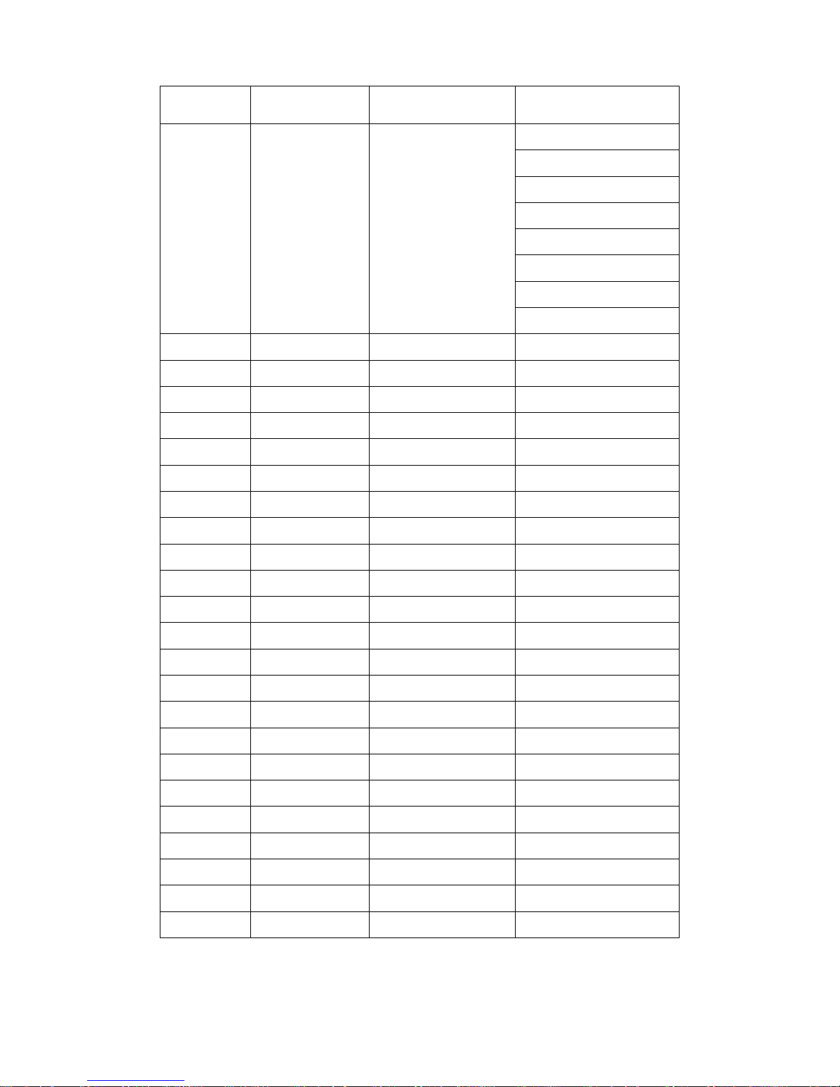
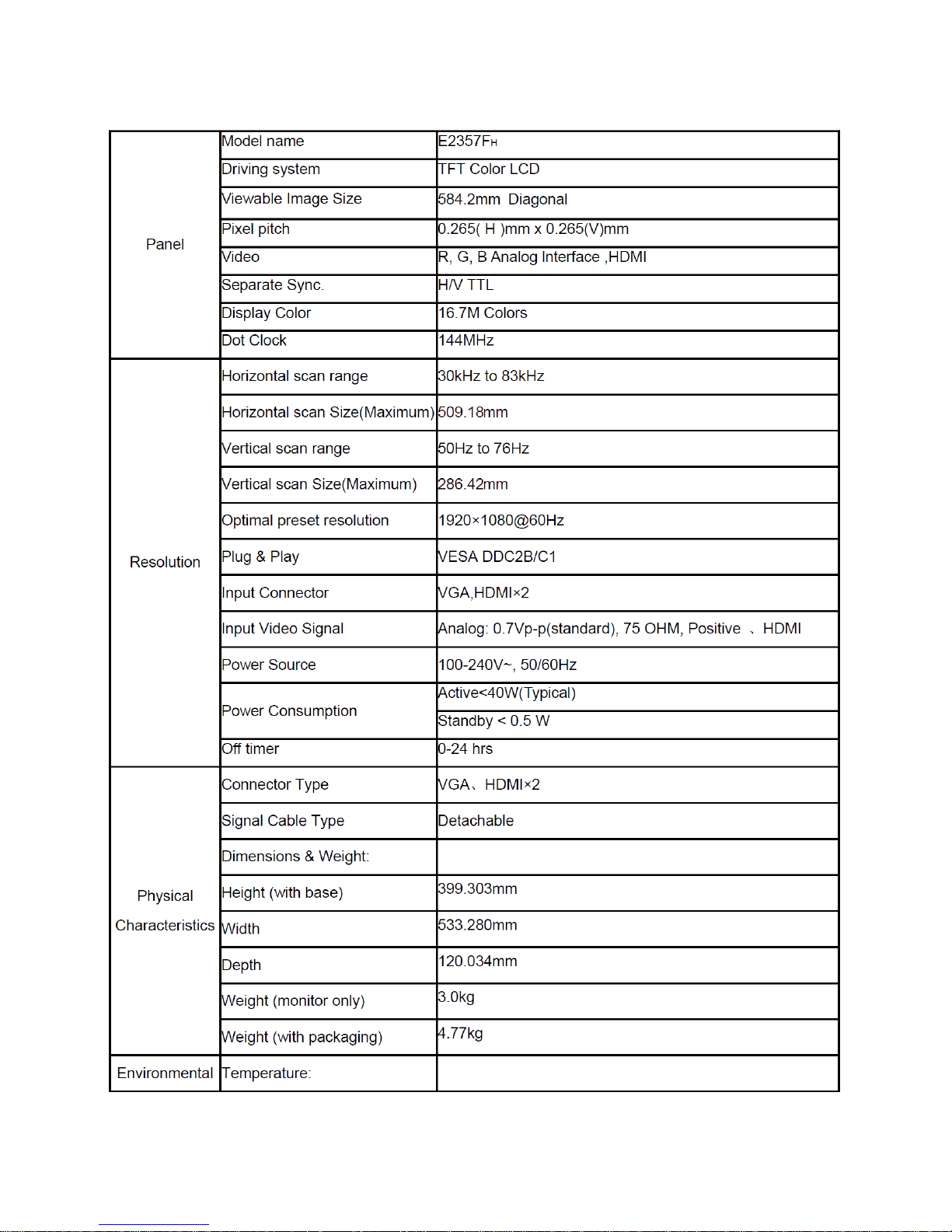
1. Monitor Specifications
Page 5
5
Page 6
6
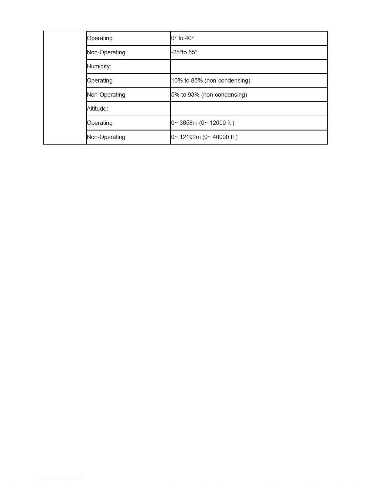
2. LCD Monitor Description
The LCD MONITOR will contain a main board and a key board which house the flat panel control logic, brightness
control logic and DDC.
Monitor Block Diagram
Flat Panel and
LED backlight
Main Board
Key Board
HDMI2
Signal
Adapter
D-SUB
Signal
AC-IN
100V~240V
LED Drive.
HDMI1
Signal
Page 7
7
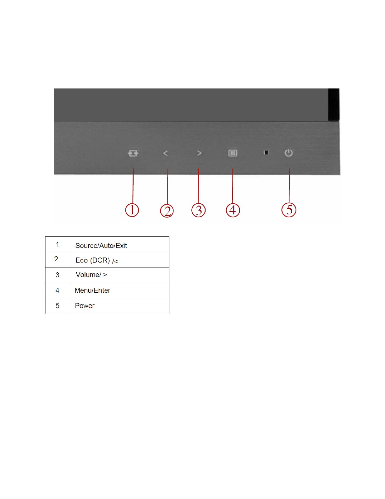
3. Operating Instructions
3.1 General Instructions
Press the power button to turn the monitor on or off. The other control knobs are located at front panel of the monitor.
By changing these settings, the picture can be adjusted to your personal preferences.
3.2 Hotkeys
Power
Press the Power button to turn on/off the monitor.
Eco(DCR)/ <
Press the Eco key continuously to select the Eco mode of brightness and DCR on when there is no OSD. (Eco mode
hot key may not be available in all models).
Volume / >
When there is no OSD, press Volume adjust volume.
Auto / Exit / Source hot key
When there is no OSD, press Auto/Source button continuously about 2 second to do auto configure.
When the OSD is closed, press Source button will be Source hot key function. Press Source button continuously to
select the input source showed in the message bar, press Menu/Enter button to change to the source selected
Page 8
8
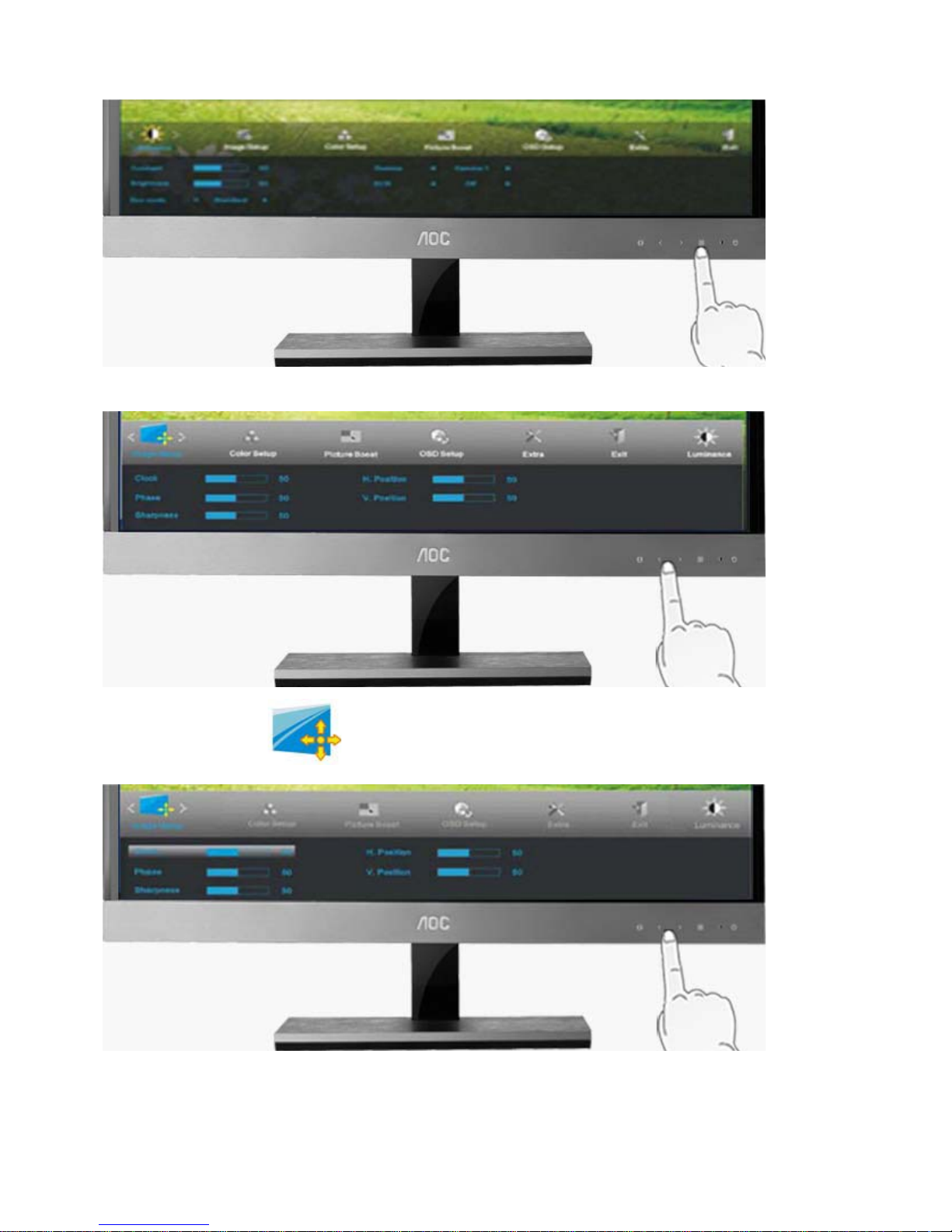
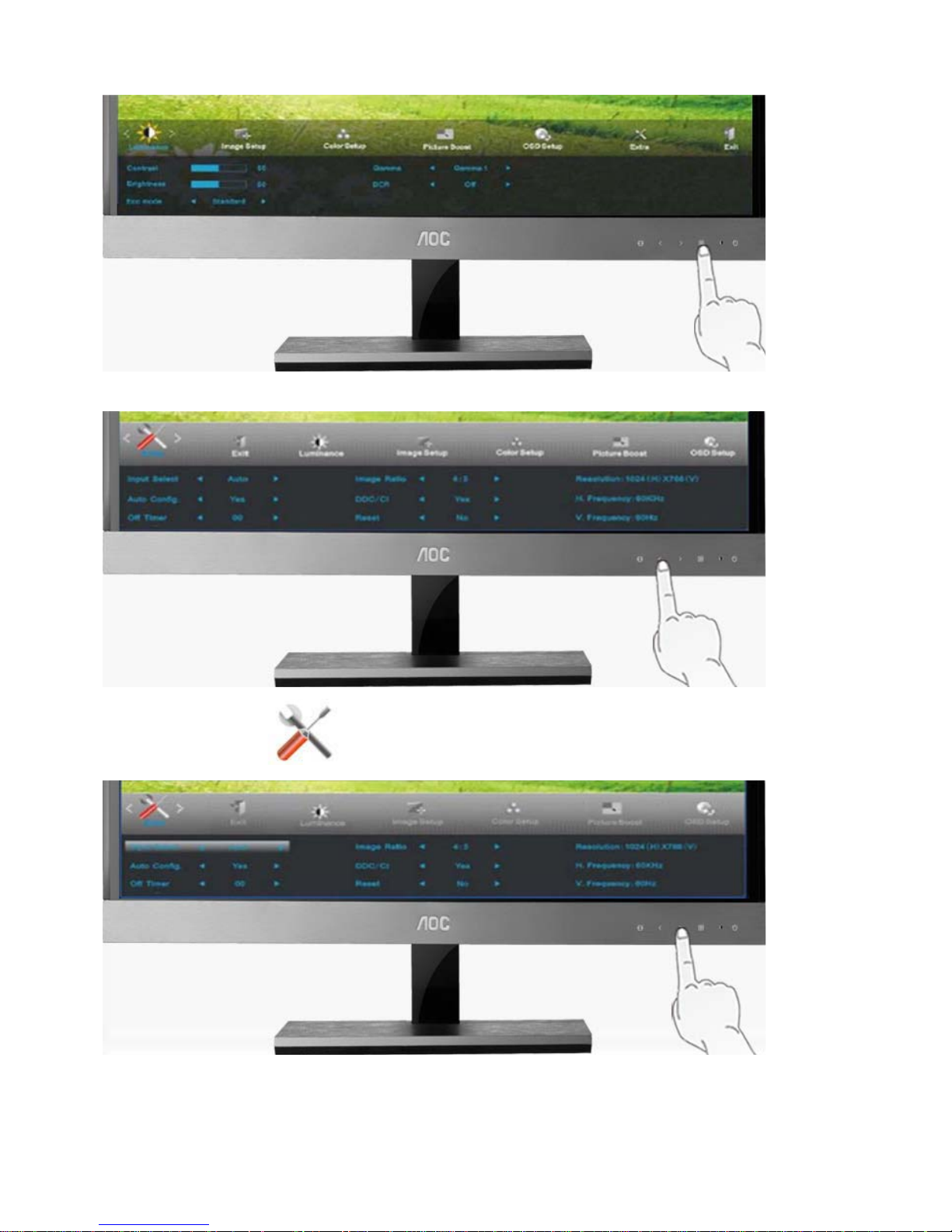
3.3 OSD Setting
Basic and simple instruction on the control keys.
1) Press the MENU-button to activate the OSD window.
2) Press < or > to navigate through the functions. Once the desired function is highlighted, press the
MENU-button to activate it . press < or >to navigate through the sub-menu functions. Once the desired
function is highlighted, press MENU-button to activate it.
3) Press < or >to change the settings of the selected function. Press AUTO to exit. If you want to adjust any
other function, repeat steps 2-3.
4) OSD Lock Function: To lock the OSD, press and hold the MENU button while the monitor is off and then press
power button to turn the monitor on. To un-lock the OSD - press and hold the MENU button while the monitor
is off and then press power button to turn the monitor on.
Notes:
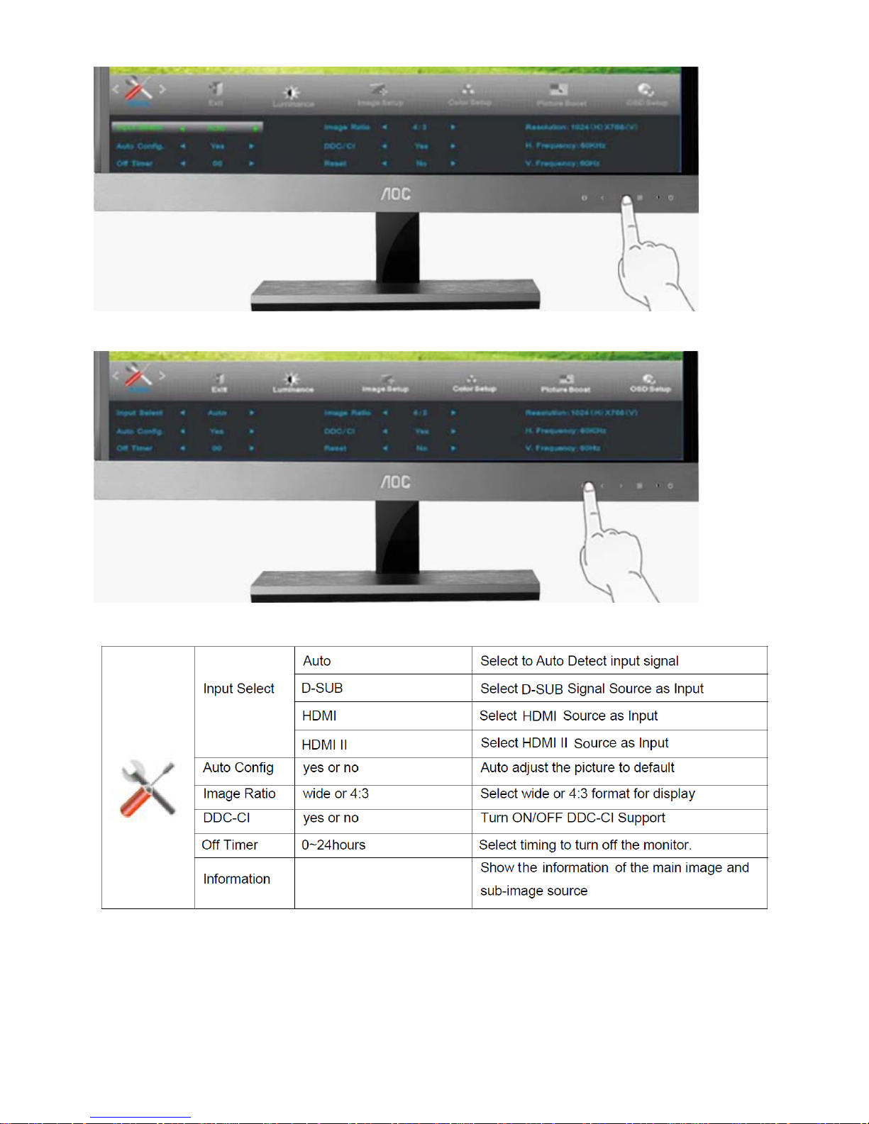
1) If the product has only one signal input, the item of "Input Select" is disable to adjust.
2) If the product screen size is 4:3 or input signal resolution is wide format, the item of "Image Ratio" is disable to
adjust.
3) One of non-standard ECO, DCR , DCB, Picture Boost is activated, the other three of functions are turned off
accordingly
Page 9
9
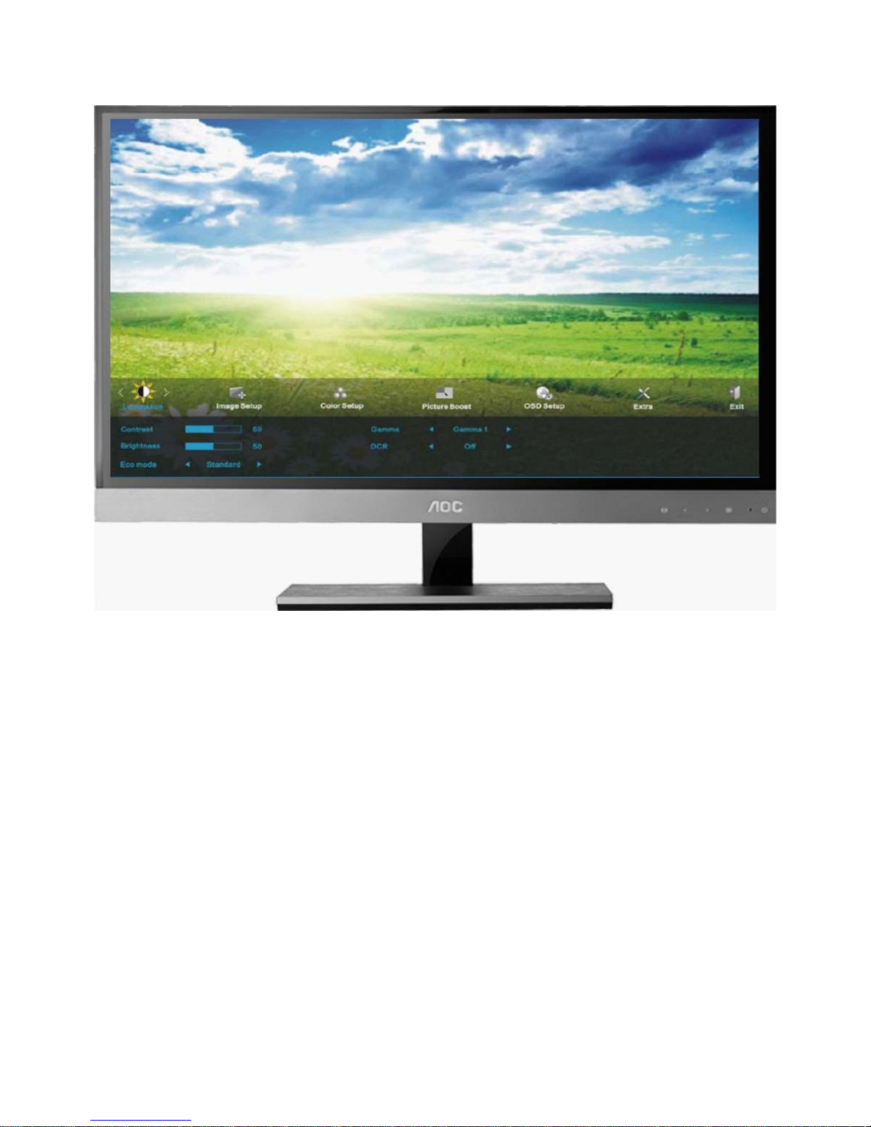
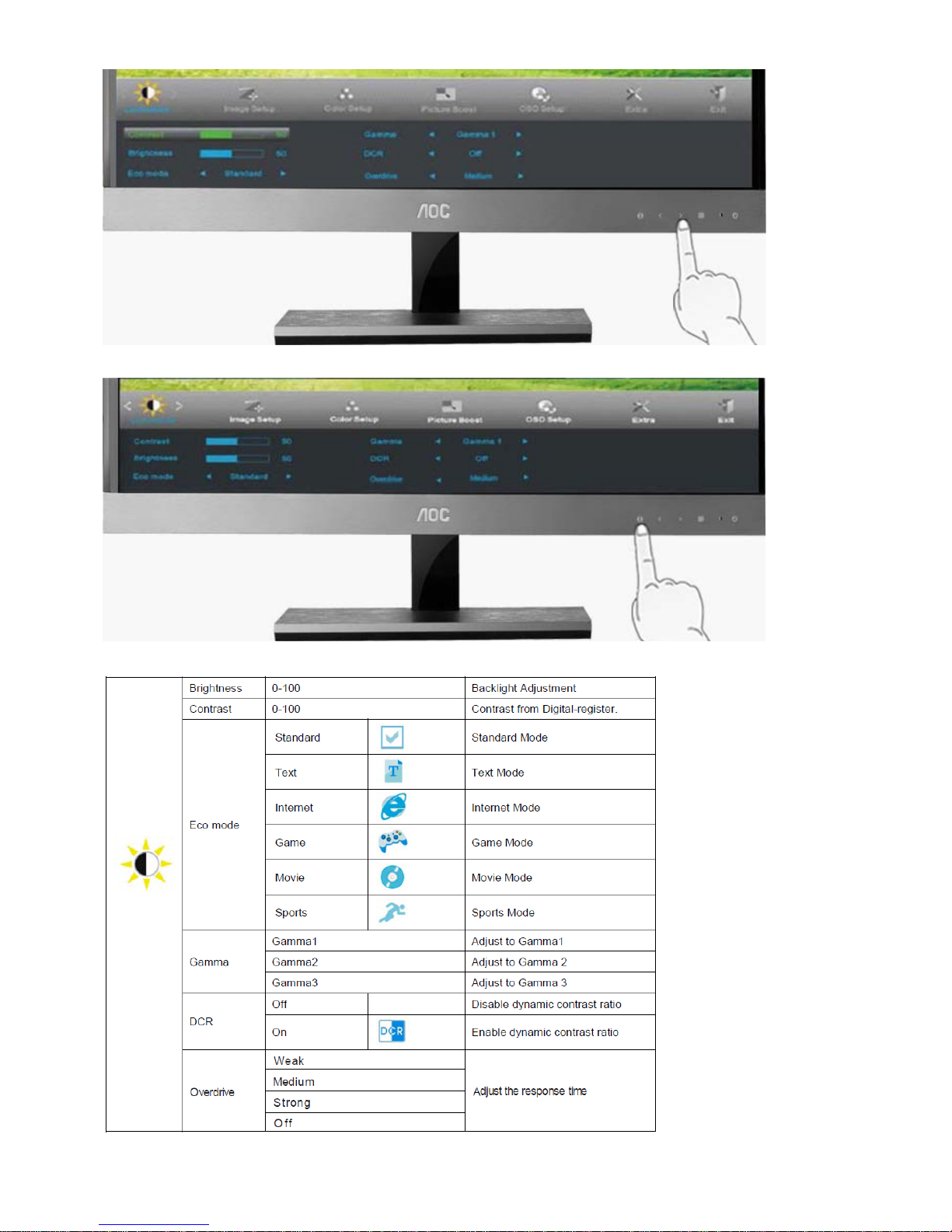
Luminance
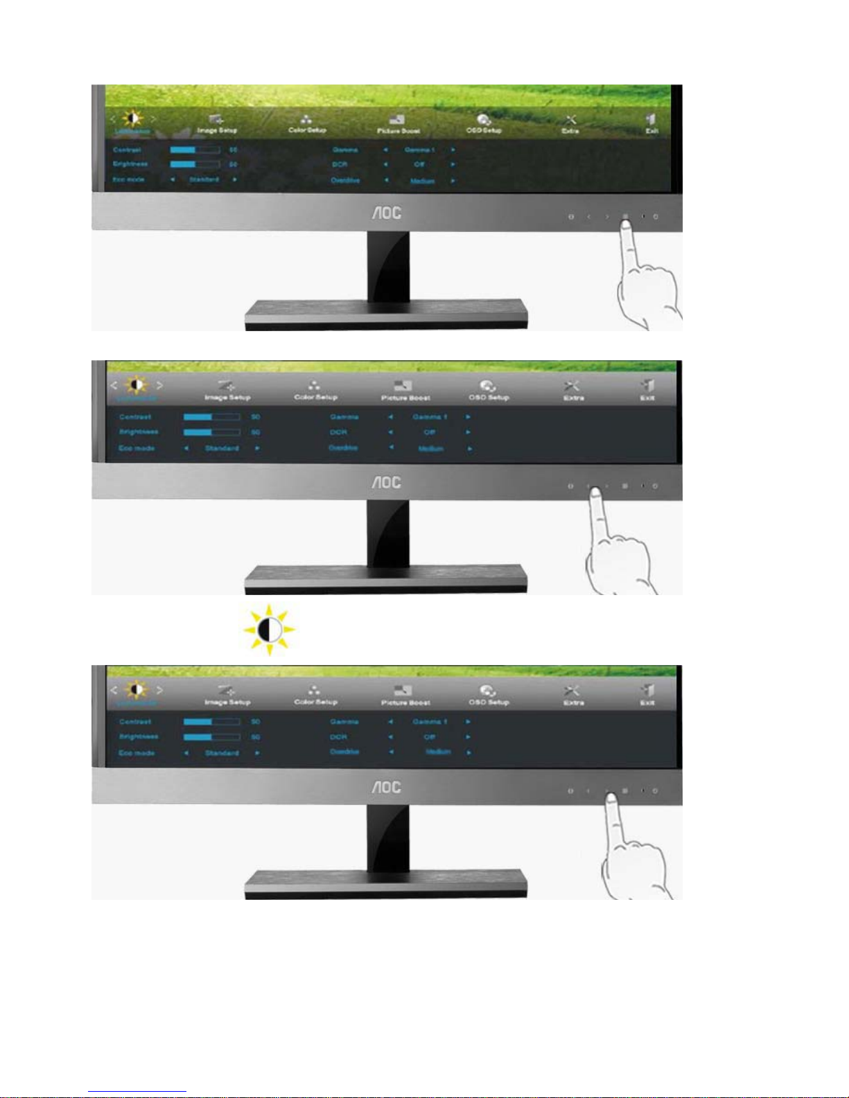
1. Press MENU (Menu) to display menu
2. Press < or > to select (Luminance), and press MENU to enter.
3. Press < or > to select submenu, and press MENU to enter.
Page 10
10
4. Press < or > to adjust.
5. Press AUTO to exit.
Page 11
11
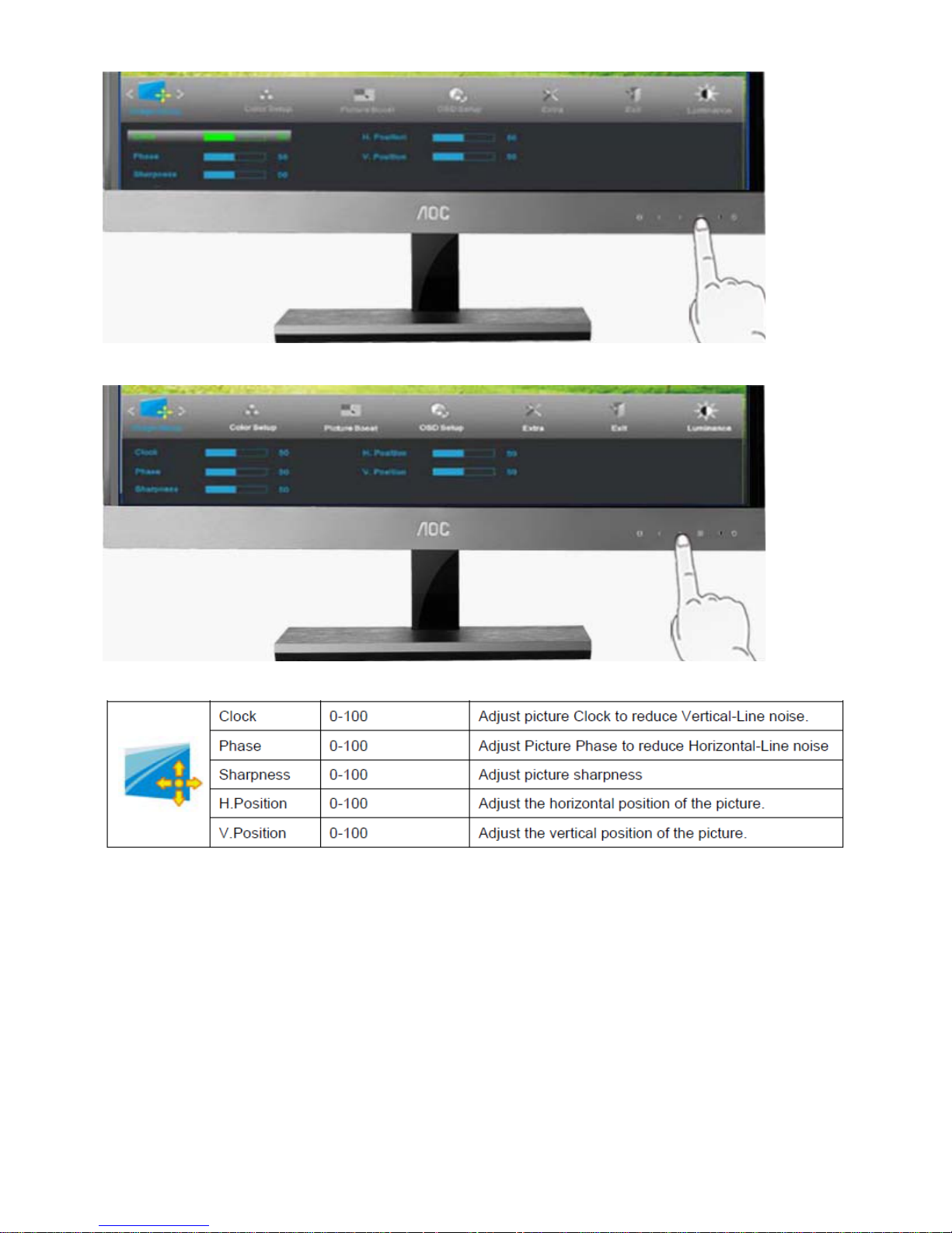
Image Setup
1. Press MENU (Menu) to display menu.
2. Press < or > to select (Image Setup) , and press MENU to enter.
3. Press < or > to select submenu, and press MENU to enter.
Page 12
12
4. Press < or > to adjust.
5. Press AUTO to exit.
Page 13
13
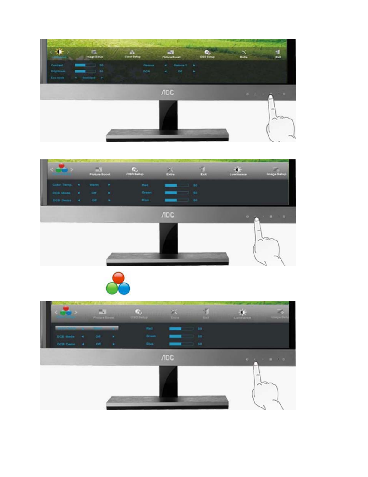
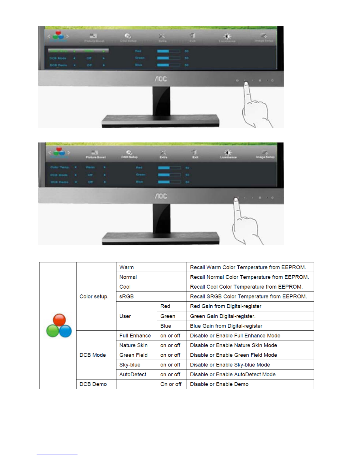
Color Setup
1. Press MENU (Menu) to display menu.
2. Press < or > to select (Color Setup) , and press MENU to enter.
3. Press < or > to select submenu, and press MENU to enter.
Page 14
14
4. Press < or > to adjust.
5. Press AUTO to exit.
Picture Boost
Page 15
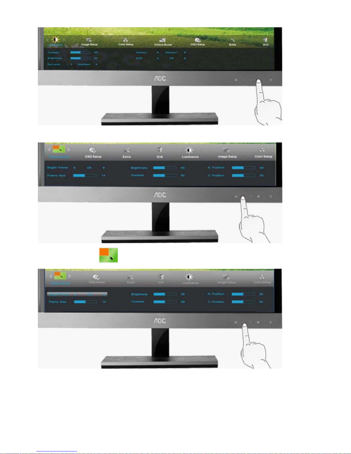
15
1. Press MENU (Menu) to display menu.
2. Press < or > to select (Picture Boost) , and press MENU to enter.
3. Press < or > to select submenu, and press MENU to enter.
Page 16
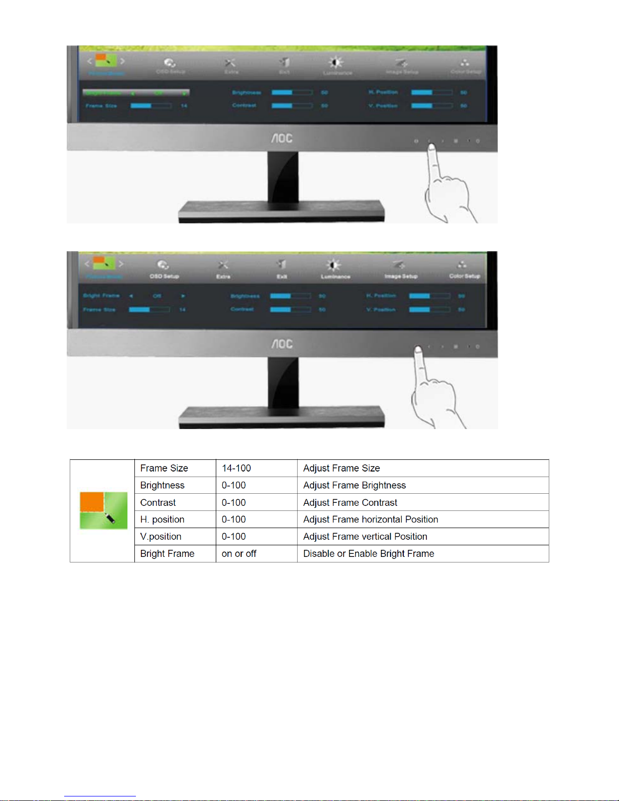
16
4. Press < or > to adjust.
5. Press AUTO to exit.
Page 17
17
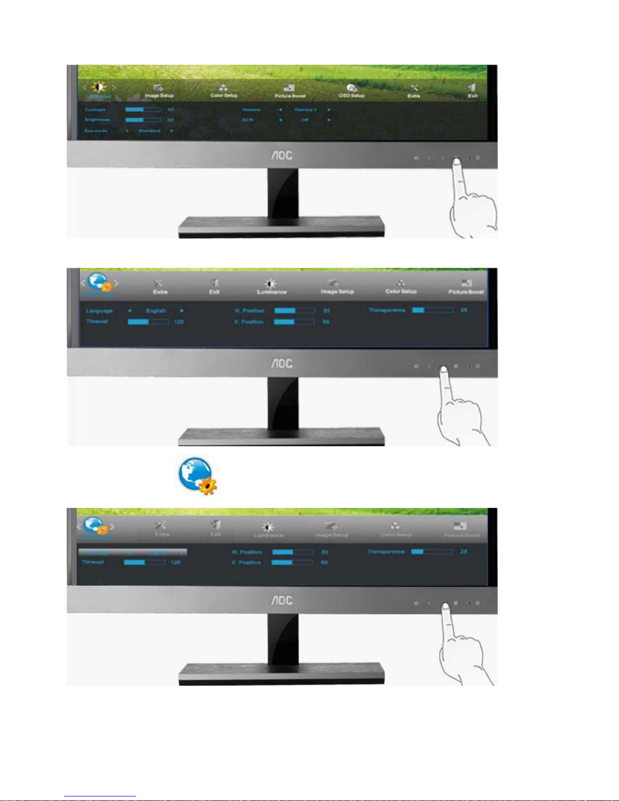
OSD Setup
1. Press MENU (Menu) to display menu.
2. Press < or > to select (OSD Setup) , and press MENU to enter.
3. Press < or > to select submenu, and press MENU to enter.
Page 18
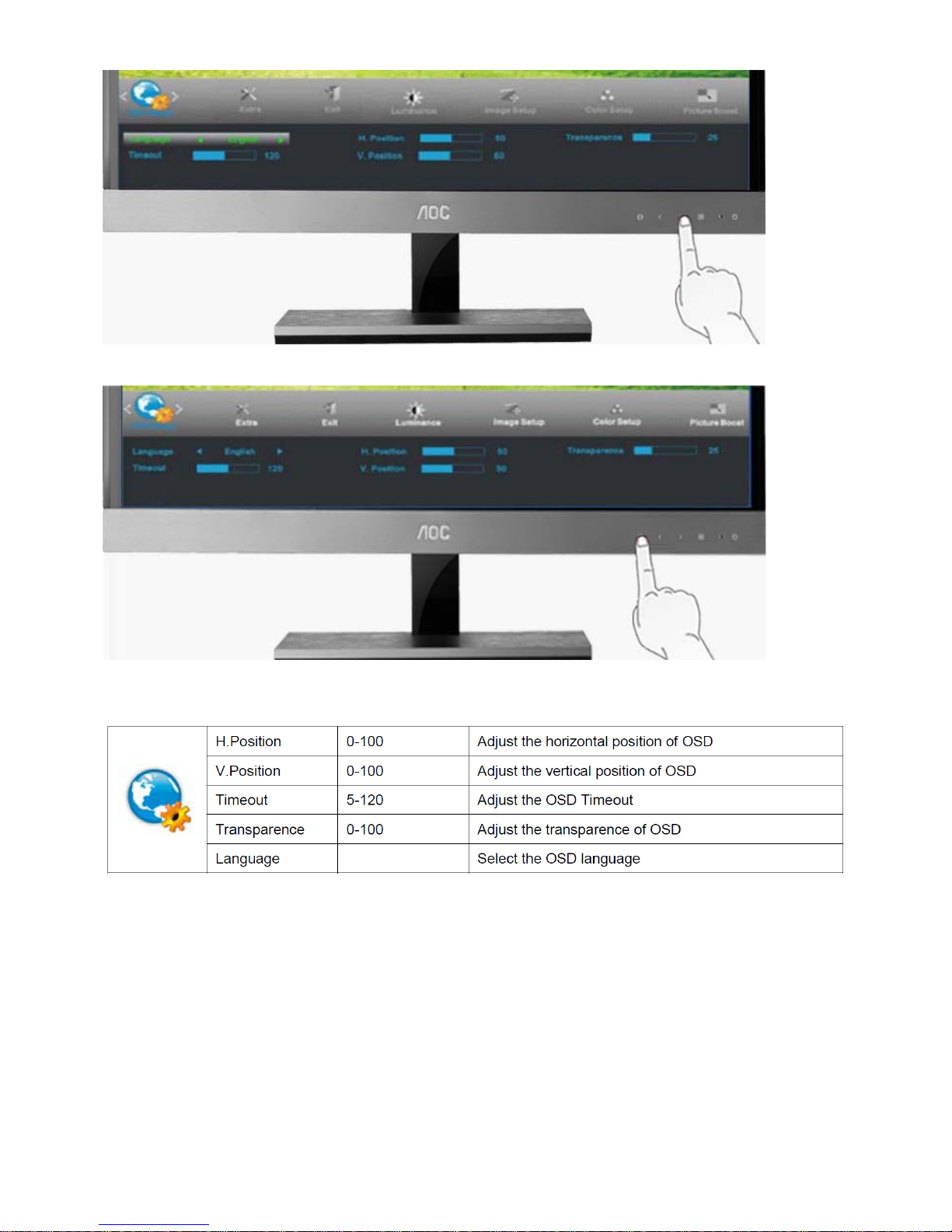
18
4. Press < or > to adjust.
5. Press AUTO to exit.
Page 19
19
Extra
1. Press MENU (Menu) to display menu.
2. Press < or > to select (Extra) , and press MENU to enter.
3. Press < or > to select submenu, and press MENU to enter.
Page 20
20
4. Press < or > to adjust.
5. Press AUTO to exit.
Page 21
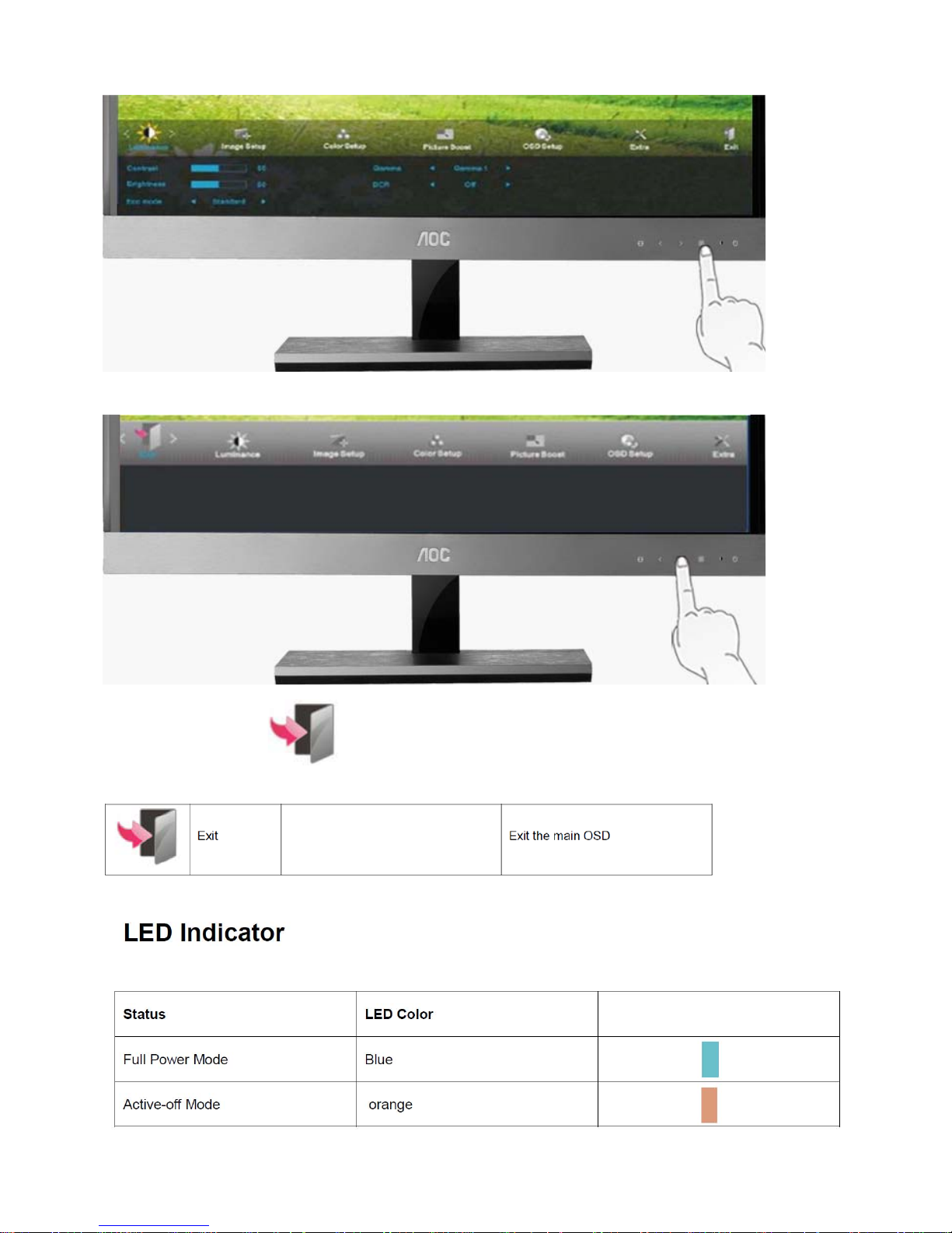
21
Exit
1. Press MENU (Menu) to display menu.
2. Press < or > to select (Exit) , and press MENU to enter.
Page 22

22
4. Input/Output Specification
4.1 D-SUB CONNECTORS and DVI CONNECTORS
Pin Assignments
Pin Number
15-Pin Side of the Signal Cable
Pin Number 15-Pin Side of the Signal Cable
Page 23

23
1
Video-Red
9 +5V
2
Video-Green
10
Ground
3
Video-Blue
11 N.C.
4 N.C. 12 DDC- Serial data
5
Detect Cable
13 H-
sync
6 GND-R 14 V- sync
7 GND-G 15 DDC- Serial clock
8 GND-B
Pin Number Signal Name Pin Number Signal Name
1
TMDS Data 2+
11
TMDS Clock Shield
2
TMDS Data 2 Shield
12
TMDS Clock
3
TMDS Data 2
13
CEC
4
TMDS Data 1+
14
Reserved (N.C. on device
5
TMDS Data 1Shield
15
SCL
6
TMDS Data 1
16
SDA
7
TMDS Data 0+
17
DDC/CEC Ground
8
TMDS Data 0 Shield
18
+5V Power
9
TMDS Data 0
19
Hot Plug Detect
10
TMDS Clock +
Page 24

24
4.2 Factory Preset Display Modes
Page 25

25
4.3 Panel Specification
4.3.1 General Features
LM230WF5-T2F2 is a Color Active Matrix Liquid Crystal Display with an integral Light Emitting Diode (LED)
backlight system. The matrix employs a-Si Thin Film Transistor as the active element. It is a transmissive type
display operating in the normally white mode. It has a 23.0 inch diagonally measured active display area with Full
HD resolution (1080 vertical by 1920 horizontal pixel array) Each pixel is divided into Red, Green and Blue
sub-pixels or dots which are arranged in vertical stripes. Gray scale or the brightness of the sub-pixel color is
determined with a 8-bit gray scale signal for each dot, thus, presenting a palette of more than 16,7M colors with
Advanced-FRC(Frame Rate Control). It has been designed to apply the interface method that enables low power,
high speed, low EMI. FPD Link or compatible must be used as a LVDS(Low Voltage Differential Signaling) chip. It is
intended to support applications where thin thickness, wide viewing angle, low power are critical factors and graphic
displays are important. In combination with the vertical arrangement of the sub-pixels, the LM230WF5-T2F2
characteristics provide an excellent flat panel display for office automation products such as monitors.
4.3.2 Display Characteristics
Page 26

26
4.3.3 Electrical Characteristics
Parameter Symbol
Values
Unit Notes
Min Typ Max
MODULE :
Power Supply Input Voltage V
LCD
4.5 5.0 5.5 Vdc
Permissive Power Input Ripple V
LCD
- - 0.3 V 3
Power Supply Input Current
I
LCD-MOSAIC
(60Hz) - 1330 1730 mA 1,5
I
LCD-BLACK
(60Hz) - 1520 1980 mA 2,5
I
LCD-BLACK
(75Hz) - 2480 mA 5
Power Consumption P
LCD
- 6.65 8.65 Watt 1
Inrush current I
RUSH
- - 3.5 A 1, 4
LED bar Electrical characteristics
Parameter Symbol Condition
Values
Unit Notes
Min. Typ. Max.
LED String Current Is - 85 90 mA 1, 2, 5
LED String Voltage Vs 40.6 44.1 47.6 V 1, 5
Power Consumption P
Bar
- 15.0 16.2 Watt 1, 2, 4
LED Life Time LED_LT 30,000 - - Hrs 3
Page 27

27
4.3.4 Optical Characteristics
(Ta=25 °C, V
LCD
=5.0V, fV=60Hz, D
CLK
=72MHz, Is=85mA)
Parameter Symbol
Values
Units Notes
Min Typ Max
Contrast Ratio CR 700 1000 -
1
(PR-880)
Surface Luminance, white LWH 200 250 - cd/m2
2
(PR-880)
Luminance Variation
WHITE
9P 75 - - %
3
(PR-880)
Response Time
Rise Time Tr
R
- 1.3 2.6 ms
4
(RD80S)
Decay Time TrD - 3.7 7.4 ms
Color Coordinates
[CIE1931]
RED
Rx
Typ
-0.03
0.638
Typ
+0.03
(PR-650)
Ry 0.331
GREEN
Gx 0.310
Gy 0.624
BLUE
Bx 0.155
By 0.066
WHITE
Wx 0.313
Wy 0.329
Viewing Angle (CR>5)
6
(PR-880)
x axis, right(?=0°)
r
75 88
Degree
x axis, left (?=180°)
l
75 88
y axis, up (?=90°)
u
70 85
y axis, down (?=270°)
d
70 85
Viewing Angle (CR>10)
x axis, right(?=0°)
r
70 85
Degree
x axis, left (?=180°)
l
70 85
y axis, up (?=90°)
u
60 75
y axis, down (?=270°)
d
70 85
Crosstalk
1.5 %
7
(PR880)
Luminance uniformity -
Angular dependence (TCO’03)
LR - - 1.7
8
(PR880)
Color grayscale linearity Δu’v’
0.018
10
(PR-650)
Page 28

28
5. Block Diagram
5.1 Main Board
DIM
ON/OFF
Feedback Circuit
D801
L801
PWM Control
OZ9998BGN
(U801)
12V
LED
(CN801)
MOSFET
(Q801)
CRYSTAL
24.576MHz
(
X401
)
Flash Memory
MX25L2026DM1I
(U402)
Scalar IC HX6823-A EPAD-LQFP-128
(Include ADC, OSD, MCU)
(U401)
Panel Interface
(CN301)
Key Control Interface
(CN405)
D-Sub Connector
(CN101)
HDMI Connector
(CN502)
HDMI Connector
(CN501)
Page 29

29
6. Schematic
6.1 Main Board
715G5240M0D000004L
C104
47nF 16V
FB101 300OHM
1 2
C105
NC/0.1UF 16V
C101
NC/0.1UF 16V
C107
47nF 16V
BIN0-
RIN0
BIN0
C109
47nF 16V
BIN0 RIN0
C110
47nF 16V
ESD_VGA
U102
L30ESDL5V0C6-4
I/O1
1
GND
2
I/O23I/O3
4
VDD
5
I/O4
6
U101
FM24C02A
A0
1
A1
2
A2
3
GND
4
SDA
5
SCL
6
WP
7
VCC
8
DDCSCL_A
DDCSDA_A
HSIN0
VSIN0 GIN0
B5
C113
47nF 16V
GND_B 5
SOG 5
DET_VGA
G5
GND_G 5
GND_R 5
VGA_5V
DSUB_H 5
+5V_AUDIO
DSUB_V 5
DDC1_SCL5
DDC1_SDA5
D101
BAV70
3
1
2
C106
22N 25V
R114 22K
VGA_CABLE_DET 5
VGA_CABLE_DET
R113 4. 7K
R101 4. 7K
R102
47R
R104
47R
U103
L30ESDL5V0C6-4
I/O1
1
GND
2
I/O23I/O3
4
VDD
5
I/O4
6
R122
2K2 1/16W 5%
R119 100R 1/16W 5%
ZD101
RLZ5.6B
VGA_5V
VGA_5V
OEM MODEL
Size
Rev
Date
Sheet
of
TPV MOD EL
PCB NAME
称爹
T P V ( Top Victory Electronics Co . , Ltd. )
Key Component
絬 隔 瓜 絪 腹
D2357Ph
B
AOC
B
28Thursday, November 24, 2011
<
称爹
>
2.0.INPU T
715G5240-M0D
GIN0
C115
NC/22pF 50V
ESD_VGA
R120 100R 1/16W 5%
R121
2K2 1/16W 5%
C114
NC/22pF 50V
RIN0-
GIN0-
BIN0-
WP_DDC3,5
R111
47R
R109
10R 1/16W 5%
R117
47R
R115
10R 1/16W 5%
C116
22PF 50V
C117
22PF 50V
ESD_VGA
+5V_AUD IO3,5,6,7
R112
1K 1/16W 5%
ZD102
RLZ5.6B
1 2
CN101 D-SUB 15P
1
6
2
7
3
8
4
9
5
11
12
13
14
15
10
17 16
BIN0
C118
0.1UF 16V
GIN0
GIN0-
RIN0-
RIN0
C119
0.1UF 16V
FB103
19 OHM 500mA
1 2
FB104
19 OHM 500mA
1 2
R105
75 OHM +-5% 1/16W
R107
1K 1/16W 5%
C103
5PF 50V
R110
75 OHM +-5% 1/16W
DDCSDA_A
C108
5PF 50V
VGA5V
DDCSCL_A
R106
47R
R103
10R 1/16W 5%
R118 0.05R
VSIN0
HSIN0
DDC1_SDA
DET_VGA
R116
75 OHM +-5% 1/16W
DDC1_SCL
VSIN0
HSIN0
FB102
19 OHM 500mA
1 2
C112
5PF 50V
C111
220nF 16V
GND_R
GND_B
GND_G
G
B
DDC1_SDA
DDC1_SCL
R108 NC/1M 1/16W 5%
C102
47nF 16V
R5
R
Page 30

30
OEM MODE L
Size
Rev
Date
Sheet
of
TPV MODEL
PCB NAME
称爹
T P V ( Top Victory Electronics Co . , Ltd. )
Key Component
絬 隔 瓜 絪 腹
D2357Ph B
AOC
C
3
8
Thursday, Nov ember 24, 2011
<
称爹
>
3.0HDMI
715G5240-M0D
U501
L30ESDL5V0C6-4
I/O1
1
GND
2
I/O23I/O3
4
VDD
5
I/O4
6
U506
L30ESDL5V0C6-4
I/O1
1
GND
2
I/O23I/O3
4
VDD
5
I/O4
6
R514
22K
U502
FM24C02A
A0
1
A1
2
A2
3
GND4SDA
5
SCL
6
WP
7
VCC
8
R513
10K
R504 0.05R
R512
10K
C503
220nF 16V
R505 0.05R
R508 0.05R
R511
1K 1/16W 5%
R502 0.05R
R515 10R 1/ 16W 5%
R506 0.05R
R509 0.05R
R507 0.05R
C504
0.1UF 16V
HDMI2_+5V
HDMI2_+5V
D501
BAT54C
C501
0.1UF 16V
C507
0.1UF 16V
WP_DDC
SHDMI1/D1-
SHDMI1/D0-
R520
NC/10K
R519
NC/10K
Q501
NC/LMBT3904LT1G
HDMI2_DET
HDMI2_+5V
SHDMI1/D1+
SHDMI1/D0+
SHDMI1/D2+
SHDMI1/CK+
SHDMI1/D2-
SHDMI1/CK-
R516 47R
R518 47R
HDMI2_HOTPLUG
R501 100R 1/ 16W 5%
R528 100R 1/ 16W 5%
R538 47R
R539 47R
HDMI2_+5V
ESD_HDMI2
HDMI2_SCL_A
R531 NC /0.05R
HDMI2_SCL_A
ESD_HDMI2
HDMI2_SDA_A
CEC_CTRL
HDMI2_SDA_A
HDMI2_DET
HDMI2_SCL_A
ZD501
RLZ5.6B
ZD505
RLZ5.6B
ZD502
RLZ5.6B
R517 1K 1/16W 5%
R537 1K 1/16W 5%
CEC_CTRL_A
ESD_HDMI1
ESD_HDMI2
R541
NC/10K
HDMI1_DET
R540
NC/10K
HDMI1_+5V
Q502
NC/LMBT3904LT1G
C502
NC/0.1UF 16V
3904
Pin11
LGE/Acer/MMD
100 ohm
3904
10K ohm
100 ohm
Pin18
ASUS/Dell/HP/Lenovo
R503 0.05R
NC
FB501 300OHM
1 2
FB502 300OHM
1 2
R539
NC
LGE(LGE design)
R538
R525
u504
AOZ8804DI
CH1
1
CH2
2
VN
3
CH3
4
CH45NC
6
NC
7
VN
8
NC
9
NC
10
NC
10K ohm
Brand
Pin11 & 18
R508
1
NC
R536
Detect pin
10K ohm
NC
SHDMI1/D0+
SHDMI1/D0-
HDMI1_DET
R537
HDMI2_+5V
HDMI1_SCL_A
10K ohm
NC
HDMI1_HOTPLUG
SHDMI1/D1+
SHDMI1/D1-
SHDMI1/D0-
HDMI1_SDA_A
SHDMI1/D0+
SHDMI1/D1+
SHDMI1/D1-
18
10K ohm
Q501
2
10K ohm
Pin11HDMI2
11
u503
AOZ8804DI
CH1
1
CH2
2
VN
3
CH3
4
CH45NC
6
NC
7
VN
8
NC
9
NC
10
100 ohm
Pin18
HDMI1
11 & 18
10K ohm
Pin11 & 18
100 ohm
C506
NC/0.1 UF 16V
Q502
3904
100 ohm
SHDMI1/D2+
SHDMI1/D2-
10K ohm
3904
SHDMI1/CK+
SHDMI1/CK-
100 ohm
SHDMI1/CK-
SHDMI1/D2-
SHDMI1/CK+
SHDMI1/D2+
RX1- 5
RXC+ 5
CN502
HDMI
TH1
20
TH2
21
D2+
1
D2 Shield
2
D2-
3
D1+
4
D1 Shield
5
D1-
6
D0+
7
D0 Shield
8
D0-
9
CK+
10
CK Shield
11
CK-
12
CE Remote
13
NC
14
DDC CLK
15
DDC DATA
16
GND
17
+5V
18
HP DET
19
TH3
22
TH4
23
TH5
24
RX2- 5
RX2+ 5
RX0- 5
RXC- 5
RX1+ 5
RX0+ 5
HDMI2_DET
HDMI2_HOTPLUG
HDMI1_+5V
HDMI2_SDA_A
HDMI1_SCL_A
R534
10K
u508
AOZ8804DI
CH1
1
CH2
2
VN
3
CH3
4
CH45NC
6
NC
7
VN
8
NC
9
NC
10
HDMI1/CK+
HDMI1/D2HDMI1/D2+
HDMI1/CK-
R532
1K 1/16W 5%
HDMI1/D2-
HDMI1/CK-
R523 0.05R
HDMI1/D2+
HDMI1/CK+
R521 0.05R
HDMI1_SDA_A
R524 0.05R
HDMI1/CK-
R522 0.05R
u507
AOZ8804DI
CH1
1
CH2
2
VN
3
CH3
4
CH45NC
6
NC
7
VN
8
NC
9
NC
10
U505
FM24C02A
A0
1
A1
2
A2
3
GND4SDA
5
SCL
6
WP
7
VCC
8
HDMI1/D0+
HDMI1/D1+
HDMI1/D1-
HDMI1/D0-
R525 0.05R
HDMI1/D1+
HDMI1/D0+
HDMI1/D0-
HDMI1/D1-
R526 0.05R
R530 0.05R
R527 0.05R
HDMI1_+5V
DET_HDMI2 5
CEC_CTRL_A
+5V_AUDIO
HDMI1/D2-
HDMI1/CK+
C510
0.1UF 16V
+5V_AUDIO
R529 0.05R
WP_DDC 2,5
HDMI1_+5V
HDMI2_SDA5
HDMI2_SCL5
HDMI1/D0-
HDMI1_DET
+5V_AUDIO 2,5,6,7
HDMI2_HPD 5
ZD504
RLZ5.6B
HDMI1_SCL5
HDMI1_SDA5
ZD503
NC/RLZ5.6B
C509
0.1UF 16V
HDMI1_HPD 5
HDMI1/D1-
DET_HDMI1 5
HDMI1_+5V
R536 10R 1/16W 5%
CEC_CTRL 5
HDMI1_D2+ 5
ESD_HDMI1
HDMI1_CK+ 5
HDMI1_D1- 5
HDMI1_D1+ 5
HDMI1/D0+
HDMI1_D0+ 5
HDMI1_D0- 5
HDMI1_D2- 5
HDMI1_CK- 5
HDMI1_SCL_A
HDMI1_SDA_A
HDMI1/D1+
R533
10K
R535
22K
C508
220nF 16V
D502
BAT54C
ESD_HDMI1
HDMI1/D2+
HDMI1_HOTPLUG
WP_DDC
C505
0.1UF 16V
R510 0.05R
CN501
HDMI
TH1
20
TH2
21
D2+
1
D2 Shield
2
D2-
3
D1+
4
D1 Shield
5
D1-
6
D0+
7
D0 Shield
8
D0-
9
CK+
10
CK Shield
11
CK-
12
CE Remote
13
NC
14
DDC CLK
15
DDC DATA
16
GND
17
+5V
18
HP DET
19
TH3
22
TH4
23
TH5
24
Page 31

31
+
C301
220uF/16V
LT-SDA 5
LT-SCL 5
+5V
C306
0.1UF 16V
PANEL_ENABLE5
VLCD
R304
100K
Q302
NC/AO3401A
R306
22K
Q301
AO4449 -7A/-30V
S1S2S3G
4
D8D7D6D
5
+5V
R305
NC
Q303
LMBT3904LT1G
C305
220nF 16V
R303
10K 1/16W 5%
R307
4.7K
C304
0.1UF 16V
VLCD
LVA1MPB7
LVA2MPB5
LVA1PPB6
LVACKMPB3
LVACKPPB2
LVA3PPB0
LVA3MPB1
PB[0..9]
LVA2PPB4
LVA0PPB8
RXO0-
LVA0MPB9
RXO1-
RXO0+
RXO2-
RXO1+
RXO2+
PA6 LVB1P
PA3 LVBC KM
PA4 LVB2P
PA0 LVB3P
PA5 LVB2M
RXOC-
PA7 LVB1M
PA[0..9]
PA1 LVB3M
RXOC+
PA8 LVB0P
RXO3+RXO3RXE0RXE1-
RXE0+
RXEC+RXEC-
RXE2+RXE2-
RXE1+
RXE3+RXE3-
LVA0P RXE0+
PA9 LVB0M
C302
NC
PA2 LVBC KP
FB301
120OHM
1 2
C303
NC
R302
300 OHM 1/4W
CN301
CONN
1
2
3
4
5
6
7
8
9
10
11
12
13
14
15
16
17
18
19
20
21
22
23
24
25
26
27
28
29
30
R301
NC/300 OHM 1/4W
LT-SDA
LT-SCL
LT-SDA
LT-SCL
LT-SDA LT-SCL
LVB2M RXO2-
RXO3-LVB3M
RXE2-LVA2M
RXO0-LVB0M
RXO1-LVB1M
LVACKM RXEC-
RXE3-LVA3M
RXOC+LVBCKP
RXE0-LVA0M
RXE1-LVA1M
RXO1+LVB1P
RXO0+LVB0P
RXE2+LVA2P
LVBCKM RXOC-
RXE1+LVA1P
RXO2+LVB2P
RXEC+LVACKP
RXO3+LVB3P
RXOC-
RXE3+LVA3P
RXEC+
RXEC-
RXOC+
CN302
NC/CONN
2
4
6
8
10
12
14
16
18
20
22
24
26
28
30
1
3
5
7
9
11
13
15
17
19
21
23
25
27
29
PA[0..9]5
OEM MOD EL
Size
Rev
Date
Sheet
of
TPV MO DE L
PCB NAME
称爹
T P V ( Top Victory Electronics Co . , Ltd. )
Key Component
絬 隔 瓜 絪 腹
D2357Ph
B
AOC Cust om
48Thursday, Nov ember 24, 2011
<
称爹
>
4.0.OU TPUT
715G5240-M0D
PB[0.. 9]5
Page 32

32
R47522R 1/16W 5%
R47822R 1/16W 5%
R47722R 1/16W 5%
FB406
120OHM
1 2
R479
NC
R480
10K 1/16W 5%
AINR7
R452 4.7K
R454 10K 1/16W 5%
on_BACKLIGHT 6
PANEL_ENABLE 4
VCCK
DACAVDD33
adj_BACKLIGHT 6
XTAL_OUT
PB7
PB8
PB9
PB2
PB3
PB4
PB5
PB6
PB[0..9] 4
PB[0..9]
PB0
PB1
C407
10uF 10V
XTAL_IN
5V_DET
USRD_MSCL
VCC3IO
C406
10uF 10V
AVDD_PLL
LED_ORANGE
EARAVDD33AVDD33_HDMI
TSTMD
USRD_MSDA
HDMI1_CK+3
FB403
120OHM
1 2
HDMI1_CK-3
AVDD3V_LV
HDMI1_SDA3
HDMI1_SCL3
U401
HX6833-A
HDMI_RXB0P
8
HDMI_RXB0N
9
HDMI_RXBCKP
10
HDMI_RXBCKN
11
HDMI_RXA2P
13
BINN
22
GINP
25
SOGIN
26
RINN
27
RINP
28
HVSS
29
HSYNC
34
VSYNC
35
DDCA_SDA/RS232_TX/GPIO31
36
DDCA_SCL/RS232_RX/GPIO30
37
SPDIF/GPIO27/IR _ctrl_out_1
60
PI
101
LVA0N
100
LVA0P
99
FMLV2N/LVA1N
98
FMLV2P/LVA1P
97
FMLVCLKN/LVA2N
96
FMLVCLKP/LVA2P
95
FMLV1N/LVACKN
94
FMLV1P/LVACKP
93
FMLV0N/LVA3N
92
FMLV0P/LVA3P
91
BMLV2P/LVB0P
87
BMLVCLKN/LVB1N
86
BMLVCLKP/LVB1P
85
BMLV1N/LVB2N
84
BMLV1P/LVB2P
83
BMLV0N/LVBCKN
82
BMLV0P/LVBCKP
81
LVB3N
80
DACVCOM/DACVCOM
69
AVDD_PLL (3.3V)
127
BINP
23
HDMI_RXA2N
14
GINN
24
BMLV2N/LVB0N
88
DACVREF
68
TSTMD
102
VCC3IO (3.3V)
103
EARAVSS33
75
SPKR/SPKR/SPKR
74
SPKL/SPKL/SPKL
73
DACAVSS33
72
LVB3P
79
HPR
77
HPL
76
XTAL_ I N
128
XTAL_ O U T
1
VCCK (1.2V)
105
DDCDB_SCL/GPIO02
115
VCCK(1.2V)
116
VCC3IO (3.3V)
118
EXT_R
3
HDMI_RXB2N
5
HDMI_RXB2P
4
HDMI_RXB1N
7
HDMI_RXB1P
6
HDMI_RXA1N
16
HDMI_RXA1P
15
HDMI_RXA0N
18
HDMI_RXA0P
17
HDMI_RXACKN
20
HDMI_RXACKP
19
PVDD2_EXTC
32
GNDIO/ GNDK (0V)46GNDIO/ GNDK (0V)57AVSS_PLL (0V)
2
VCC3IO (3.3V)
45
AVSS33 (0V)
21
VCCK (1.2V)
47
GNDIO/ GNDK (0V)
104
AVSS3V_LV(0V)/PVSS3V_LV(0V)
90
AVDD3V_LV(3.3V)/PVD D3V_LV(3.3V)
89
EARAVDD33
78
RST_N
122
AVDD33_HDMI
12
HVDD
30
DDCDA_SCL/GPIO14
121
DDCDA_SDA/G PIO13
120
PVDD1_33
31
PVSS1_33
33
DACAVDD33
67
SAR0/GPIO20
123
SAR1/GPIO21
124
SAR2/GPIO22
125
SAR3/GPIO23
126
PAD_RAIN0B
71
PAD_LAIN0B
70
SDI
106
CSN
107
SCK
108
SDO
109
DDCDB_SDA/G PIO01
114
GNDK/GNDIO (0V)
117
USRD_MSDA/GPIO1 5/I2S_SCK
111
USRD_MSCL/GPIO16/I2S_WS
112
VCC3IO (3.3V)
58
VCCK(1.2V)
56
GVON/GPIO40/I2S_SCK/sy nc_3d_out_0
61
OEV/GPIO41/I2S_WS/sy nc_3d_out_1
62
CPV/GPIO42/I2S_SD0/s ync_3d_out_2
63
STV1/GPIO43/I2S_SD1/sy nc_3d_out_3
64
FTP/GPIO44/I2S_SD2/sy nc_3d_out_4
65
POL/GPIO17/I2S_SD3/sy nc_3d_out_5
66
GPIO03/PWMB//I2S_SD2/sync_protect
48
GPIO04/PWMC//I2S_SD3/sys_pwdn_1p2v_en
49
PWMB/GPIO10//PWM_dbl
51
PWMC/GPIO11/CMI_3d_in
52
PWMD/GPIO12/CMI_3d_duty _in
53
GPIO24/sync_3d_out_l
54
GPIO00/CEC
110
GPIO05
50
GPIO06
119
GPIO07
113
GPIO31/RS232_TX/I2S_SD0/PWM_OUT_LED
43
GPIO30/RS232_RX/I2S_SD1/PWM_OUT_LED
44
CEC/GPIO26/IR_ct rl_out_0
59
GPIO02/SPDIF
39
GPIO25/sync_3d_out _r
55
GPIO36//PWMC/CMI_3d_in
41
GPIO37/PWMD/CMI_3d_duty _in
42
GPIO35//PWM_dbl/PWM_B
40
GPIO01/CEC/12v _pwdn_en
38
EPAD
129
R449 100R 1/16W 5%
R433NC/10K 1/16W 5%
RXC-3
FB404
120OHM
1 2
RX2-3
RX2+3
RXC+3
RX0+3
RX1-3
RX1+3
RX0-3
HDMI2_SCL3
HDMI2_SDA3
SCK
CSN
SDI
R424 100R 1/16W 5%
SDO
PA8
PA9
PA3
PA4
PA5
PA6
PA7
PA[0..9] 4
PA[0..9]
PA0
PA1
PA2
HVDD
PVDD1_33
RST_N
R439 NC/100R 1/16W 5%
GND_G2
B2
GND_B2
GND_R2
SOG2
G2
C447
10uF 10V
R425 0.05R
R2
R428 0.05R
DSUB_H2
FB409
120OHM
1 2
AINL7
DSUB_V2
R420 100R 1/16W 5%
DDC1_SCL2
DDC1_SDA2
R487 NC/100R 1/16W 5%
LED_GRN/BLUE
R488 NC/100R 1/16W 5%
SPI_WP#
WP_DDC2,3
R40110R
FB402
120OHM
1 2
EE_WP
FB401
120OHM
1 2
R416 100R 1/16W 5%
VGA_CABLE_DET2
R404
390R 1/16W 5%
FB407
120OHM
1 2
SPI_WP#
IR_IN
C445
220nF 16V
FB405
120OHM
1 2
VCC3.3
HDMI1_HPD 3
HDMI2_HPD 3
FB408
120OHM
1 2
C446
NC/5pfF 16V
DET_HDMI23
R393 47R
R392 47R
VCC3.3
R389
4.7K
LT-SDA 4
LT-SCL
LT-SCL 4
LT-SDA
R388
4.7K
X401
24.576MHz
C402
20pF
C401
20pF
AUDIO_SD 7
DET_HDMI13
DET_HDMI1 3
DET_HDMI2 3
R417 0.05R
AUDIO_MUTE 7
Volume 7
VCC3.3
CEC_CTRL 3
C415
0.1UF 16V
PVDD1_33
AVDD_PLL
C435
0.1UF 16V
C413
0.1UF 16V
Close to HR3
AUDIO OUT
Close to HR3
VCC3.3
C433
10uF 10V
AVDD3V_LV
VCC3.3
R421 0.05R
VCC3IO
AUDIO DAC 3.3V
VCC3.3
C440
0.1UF 16V
Close to HR3
AVDD33_HDMI
C439
0.1UF 16V
EARAVDD33VCC3.3
Close to HR3
EAR HPONE 3.3V
VCC3.3
C411
0.1UF 16V
HVDD
Close to HR3
C438
0.1UF 16V
Close to HR3
VCC3.3
CN403
NC/CONN
1
2
3
4
5
6
7
89
DACAVDD33
CN401
NC/CONN
1
2
3
4
5
6
7
8
910
CN405
CONN
1
2
3
4
5
6
78
Close to HR3
C430
0.1UF 16V
C432
0.1UF 16V
VCC3.3
VCC3.3
C441
0.1UF 16V
C417
0.1UF 16V
Close to HR3
R441 100R 1/16W 5%
R443 100R 1/16W 5%
R445 100R 1/16W 5%
KEY1
KEY2
POWER_KEY#
C449
10uF 10V
C448
10uF 10V
Close to HR3
VCC1D2
C423
0.1UF 16V
R457
4.7K
VCCK
C420
0.1UF 16V
R458
4.7K
VCCK
C422
0.1UF 16V
C421
0.1UF 16V
VCC3.3
RESET
RST_N
C403
1UF 10V
VCC3.3
R405
10K 1/16W 5%
IR_IN
LED_G
R403
1MOHM 1/16W +/-5%
DET_HDMI1
X1 GROUNG
SHIELDING
VCC3.3
R438
NC/27K
D402NC
132
USER DATA
R467
NC/3K9 +/-5% 1/16W
R468
NC/3K9 +/-5% 1/16W
POWER_KEY#
C428 N C/100N16V
CN404
NC/CONN
1
2
3
4
5
6
7
C405 10UF
CN402
NC/CONN
1
2
3
4
5
6
R464 0.05R
R462 NC
C424 N C/0.1UF 16V
C427 N C/100N16V
D401 NC/RLZ5.6B
C442
NC/100N 16V
LED_R
LED_R
TOUCH_POWER
FB411
NC/120 OHM
1 2
C425 N C/0.1UF 16V
C426 N C/100N16V
R463 0.05R
FB410
NC/120 OHM
1 2
VCC3.3
R461 NC
VCC3.3
VCC3.3
DET_HDMI2
KEY1
R469
NC/3K9 +/-5% 1/16W
KEY2
VCC3.3
R410
2K2 1/16W 5%
VCC3.3
R409 NC/0R05 1/16W
LED_GRN/BLUE
R411
4.7K
+5V_AUDIO
+5V_AUDIO2,3,6,7
R412
NC/100R 1/10W 5%
LED_RLED_G
R414
NC/100R 1/10W 5%
Q401
LMBT3906LT1G
+5V_AUDIO
R408 0.05R
R415
0.05R
LED_ORANGE
Q402
LMBT3906LT1G
+5V_AUDIO
R413
200R
R407 0.05RR406 NC
C450
10uF 10V
SPKR
SPKL
R456
4.7K
R481
NC/100K
R482
NC/200K
U402
MX25L2026DM1I-12G
CS
1
SO
2
WP
3
GND4SI
5
SCK
6
HOLD
7
VCC
8
5V_DET
+5V_AUDIO2,3,6,7
AOUT_L 7
AOUT_R 7
R459NC/10K 1/16W 5%
R460NC/10K 1/16W 5%
R46515K 1/16W 5%
R46615K 1/16W 5%
C409
220pF 50V
C408
220pF 50V
D405 RLZ5.6B
1 2
R40210R
XTAL_I N
XTAL_O U T
D404 RLZ5.6B
1 2
SPI FLASH
D403 RLZ5.6B
1 2
R486 NC/10K 1/16W 5%
OEM MODEL
Size
Rev
Date
Sheet
of
TPV MODEL
PCB NAME
称爹
T P V ( Top Victory Electronics Co . , Ltd. )
Key Component
絬 隔 瓜 絪 腹
B
AOC
Custom
58Thursday, Nov ember 24, 2011
<
称爹
>
5.0.SCALER
715G5240-M0D
D2357Ph
HDMI1_D0-3
HDMI1_D0+3
SCK
CSN
SDO
SDI
R490 100R 1/16W 5%
R489 100R 1/16W 5%
SPKR
SPKL
HDMI1_D1-3
HDMI1_D1+3
HDMI1_D2+3
HDMI1_D2-3
AVDD33_HDMI
+5V_AUDIO
EE_WP
USRD_MSDA
U403
NC/24LC02BT-I/SN
A0
1
A1
2
A2
3
VSS4SDA
5
SCL
6
WP
7
VCC
8
VCC3.3
USRD_MSCL
R471NC/4K7 1/16W 5%
C443
NC/220nF 16V
R483 NC/100R 1/16W 5%
R472NC/4K7 1/16W 5%
R470NC/4K7 1/16W 5%
R47622R 1/16W 5%
R484 NC/100R 1/16W 5%
Page 33

33
R712
10K +-1% 1/10W
R708
53.6KOHM +-1% 1/10W
C712
100pF 50V
R707
10R 1/10W 5%
C720
22PF 50V
R710
30K 1/16W
C722
2N2 50V
+
C702
470uF 16V
R714
4.7K
C711
1uF 16V
L701
10uH
R709
100K
L702
10uH
+5V 4
BKLT-EN8
BKLT-VBR18
U701
G5725ADJT11U
VIN
4
EN
1
LX
3
VFB
5
GND
2
C718
1uF 16V
on_BACKLIGHT 5
adj_BACKLIGH T 5
Q701
LMBT3904LT1G
R703
51K 1%
R705
11.5K 1%
L703 22UH
R706
51K 1%
D701
SR34
1 2
R711
33K
C713
10uF 25V
C717
0.1UF 16V
+
C716
470UF 16V
VCC3.3
R702
100 OHM 1/10W
+
C704
470uF 16V
+5V_AUDIO 2,3,5,7
C729
10uF 10V
C709
10N 50V
C706
10N 50V
C710
2U2 16V
U702
G5725ADJT11U
VIN
4
EN
1
LX
3
VFB
5
GND
2
VCC1D2
ZD701 ZM-PTZ9.1BST 9.1B
12
D702
SR34
1 2
+
C723
150UF 25V
C728
10uF 10V
C715
NC/10uF 25V
+5V
C714
0.1UF50 V
+5V_AUDIO
C725
0.1UF50V
+5V_AUDIO
+5V_AUDIO 2,3,5,7
R704
51K 1%
2010/1/25
2010/2/25
C719
0.1UF 16 V
+12V
BKLT-EN
FB701
BEAD
1 2
C708
2U2 16V
C703
10N 50V
+12V 7,8
R713
10K 1/16W 5%
C726
NC/100N 16V
R717 22K
R716 100R 1/16W 5%
+5V_AUDIO
VCC3.3
R715
10K 1/16W 5%
C730
NC/0. 1UF50V
CN701
JACK
3
2
1
C707
10N 50V
R701
100 OHM 1/10W
Vout=0.6(1+R703/R705)=3.26
ZD702
NC/RLZ6.2B
1 2
OEM MODEL
Size
Rev
Date
Sheet
of
TPV MOD EL
PCB NAME
称爹
T P V ( Top Victory Electronics Co . , Lt d. )
Key Component
絬 隔 瓜 絪 腹
e2357Phz
B
AOC
B
68Thursday , Novem ber 24, 2011
<
称爹
>
6.0.POW ER
715G5240-M0B
C721
100pF 50V
Vout=0.6(1+R704/R706)=1.2
U703
APW7080KAI TRL
VIN
1
EN
2
UGND
3
VCC4LX
5
COMP
6
FB
7
GND
8
LX
9
C724
1N 50V
VCC3.3
Page 34

34
C617
1UF 10V
C623
0.1UF 16V
R604 110R 1/10W 5%
+5V_AUDIO
R602 110R 1/10W 5%
AOUT_L5
R606
100R 1/16W 5%
Volume5
C630
APA2606NI
R622
1K
7500OHM
NC
12K
R641
NC
R627
NC
C632
Thernal pad
3K
1U
PAM8007HNR
NC
NC
NC
Yes
R640
R643
R642 33K
0.47U
NC
NC
NC
0.47U
AOUT_R5
0OHM
No
NC
R644
R645
0OHM
C631
30K
C641
1UF 10V
R646
12K 1% 1/16W
R647 NC/750R 1/10W 5% R648 NC/750R 1/10W 5%
OEM MODEL
Size
Rev
Date
Sheet of
TPV MODEL
PCB NAME
称爹
T P V ( Top Victory Electronics Co . , Ltd. )
Key Component
絬 隔 瓜 絪 腹
D2357Ph B
AOC
Custom
78Thursday, Nov ember 24, 2011
<
称爹
>
7.0.AUDIO
715G5240-M0D
OUTL
OUTR
R649
NC/300 OHM
+
C631
470UF 16V
R625
NC/100K 1/16W 5%
R619
1K 1/16W 5%
U601
APA2606NAI-TRG
LOUTP
1
PGND2PGND
3
LOUTN
4
PVDD
5
MUTE
6
VDD
7
LINN
8
UVP
9
VDC
10
VOLUME
11
HP_LOUT
12
HP_ROUT13BYPASS14SE/BTL15AGC16RINN17GND18SD19PVDD20ROUTN21PGND22PGND23ROUTP
24
Thernal Pad
25
SE
R612 3K 1/16W
+
C616
220uF/16V
+
C615
220uF/16V
+5V_AUDIO
C607
1UF 10V
C606
1UF 10V
C619
220pF 50V
C626
220pF 50V
FB603 120OHM
1 2
FB604
120OHM
1 2
FB606 120OHM
1 2
C611
220pF 50V
FB605 120OHM
1 2
OUT-R-
C614
220pF 50V
OUT-R+
OUT-L-
OUT-L+
C612
NC/220pF 50V
C621
NC/220pF 50V
R613 33K
VOL
C618
1UF 10V
C622
10uF 10V
+5V_AUDIO
VCC3.3
C610
1UF 10V
C608
10uF 10V
+5V_AUDIO
C625
0.1UF 16V
C637
0.1UF50V
C634
0.1UF 16V
C636
10uF 25V
C620
10uF 25V
Q602
LMBT3906LT1G
1
23
R637
10K +-1% 1/10W
+5V_AUD IO
R614 0.05R
U602
APW7080KAITRL
VIN
1
EN
2
UGND
3
VCC4LX
5
COMP
6
FB
7
GND
8
LX
9
D601
LL4148
C639
NC/1N 50V
R635
30K 1/16W
R632
NC/0R05 1/10W
C632
1uF 25V
R631
10K 1/16W 5%
Q601
LMBT3904LT1G
ZD601 ZM-PTZ9.1BST 9.1B
12
C640
2N2 50V
+12V
+5V_AUDIO
R628
22K
R636
33K
C630
100pF 50V
C629
1uF 25V
MUTE-1
C628
0.1UF 16V
R623
10K 1/16W 5%
AUDIO_MUTE5
+12V
ZD602
NC/RLZ6.2B
1 2
R626 470R 1/16W 5%
C633
NC/10uF 25V
R627 10K 1/ 16W 5%
+12V 6,8
R622
1K 1/16W 5%
R633
100K
R624
NC/10K1/16W
R634
53.6KOHM +-1% 1/10W
D602
SR34
1 2
C638
0.1UF 16V
L601 22UH
+5V_AUDIO
C635
22PF 50V
R611NC/33K
R617
NC/750R 1/10W 5%
R608
1K 1/16W 5%
R609
1K 1/16W 5%
OUTL
AINL
CN601
PHONEJACK
1
2
3
5
4
G-2
C6046.8nF 50V
FB602
120OHM
1 2
R603 100R 1/16W 5%
R618 NC/750R 1/10W 5%
C603 0.47uF 16V
R610NC/33K
C602 0.47uF 16V
CN602
PHONEJACK
1
2
3
5
4
AINR
R601
100K
G-1
AINR 5
OUTR
OUTL
AINL 5
OUTR
R620
1K 1/16W 5%
C6056.8nF 50V
SE
FB601
120OHM
1 2
C609 0.47uF 16V
C613 NC/0.47uF 16V
R605
10K 1/16W 5%
C601
1uF 16V
R607
10K 1/16W 5%
VOL
D603
SR34
1 2
CN603
CONN
1
2
3
4
5 6
+12V6,8
AUDIO_SD 5
R621
1K 1/16W 5%
MUTE-1
+5V_AUDIO
R645 30K OHM +-1% 1/16W
C624 0. 47uF 16V
C627 N C/0.47uF 16V
Page 35

35
ISEN1
ISEN2
ISEN4
ISEN3
+
C801
150UF 25V
ISEN3
ISEN2
ISEN4
ISEN1
+12V
+12V6,7
BKLT-VBR16
BKLT-EN6
D801
B3100B
1 2
R817
7.15K 1%
CN803
NC/CONN
2
4
6
1
3
5
R815
6.2KOHM +-1% 1/10W
CN802
NC/CONN
1
2
3
4
5
6
OEM MOD EL
Size
Rev
Date
Sheet
of
TPV MODEL
PCB NAME
称爹
T P V ( Top Victory Electronics Co . , Ltd. )
Key Component
絬 隔 瓜 絪 腹
D2357Ph B
AOC
B
88Wednesday , February 08, 2012
<
称爹
>
8.0.CON VERT
715G5240-M0D
ISEN2
ISEN1
ISEN4
ISEN3
CN801
CONN
1
2
3
4
5
6
7
8
9
10
1112
VLED
VLED
C813
NC
C808
2N2 50V
C806
2N2 50V
R801
10 OHM 1/4W
U801
OZ9998BGN
ISEN1
13
ISEN2
14
GND
15
ISEN316ISEN4
1
ISET
2
OVP
3
RT
4
ENA
5
ISW
6
LDR
7
VREF
8
VIN
9
STATUS
10
SSTCMP
11
PWM
12
R819 1R
C809
390P 50V
R818 1R
R809
10K
R810
0.1R 1%
R802
0 OHM 1/4W
R820 1R
R814
300K
C807
0.47UF 50V
R821 1R
Q801
AOD482
R808
470R
C814
1N 50V
C816
2.2UF
C812
220NF 25V
R813
5K1 1/10W 1%
C802
0.1UF50V
C805
1uF 16V
C817
1N 50V
R807 10R
R816
330K
R805
300K
R804
160K 1%
C815
0.47UF 50V
C803
0.47UF 50V
R811
0.2oHM 1% 1/4W
R812
100 OHM 1/10W
C810
NC
R806
100K
+
C804
33UF 100V
R803
10K
C811
100pF 50V
L801
47UH
C818
0.47uF 16V
Page 36

36
6.2 Key Board
715G4842K0E000004F
5V_LED
DATA
SM_CLK
SM_INT#
R006 0R05 1/16W
ZD001
UDZSNP5. 6B
1 2
ZD002
UDZSNP5.6B
1 2
CN001
CABLE
1
2
3
4
5
6
R005 0R05 1/16W
CIN_03
CIN_07
CIN_11
5V_LED
CIN_01
+
-
R007
4K7 1/16W 5%
V3.3
R008
4K7 1/16W 5%
OEM MOD EL
Size
Rev
Date
Sheet
of
TPV MOD EL
PCB NAME
称爹
T P V ( Top Victory Electronics Co . , Ltd. )
Key Component
絬 隔 瓜 絪 腹
e943Fw C
AOC e943Fw
A3
22Tuesday, April 19, 2011
715G4164-K0C
<
称爹
>
2.0 Touch key
715G4164-K0C-000-0040_20100420. DSN
R003
4K7 1/16W 5%
R004
100R 1/16W 5%
C004
12P 50V
C008
100P 50V
C007
100nF 25V
CIN_01
Dif ferential KEY0.1524
CIN_05
C005
100nF 25V
Differential
C006
100nF 25V
GPIO_00
SM_CLK
U001
IT7230EFN/BX
CIN03
1
CIN07
2
CIN09
3
CIN11
4
VSHILD5VBIAS6AVSS7AVCC
8
DVCC
9
SCLK
10
SDA
11
INT#
12
GPIO013GPIO1
14
CIN0015CIN01
16
E-PAD
17
CIN_09
Auto
CIN_03
-
SM_INT#
SM_DATA
CIN_05
GPIO_01
Power
V3.3
V3.3
Menu+
AC_SHIELD
VBIAS
Auto
Power
R001
10K 1/16W 5%
C003
12P 50V
CIN_11
AC_SHIELD
CIN_07CIN_09
AUTO_4
KEY0.1524
-_2 KEY0.1524
Orange
Blue
D001
2
3
1
MENU_5 KEY 0.1524
+_3
KEY0.1524
R002
4K7 1/16W 5%
PWR_1 KEY0. 1524
GPIO_01
GPIO_00
TP2
KEY0.1524
VBIAS
MENU
CLK
C011
1UF 10V
V3.3
SM_DATA
Page 37

37
7. PCB Layout
7.1 Main Board
715G5240M0D000004L
Page 38

38
Page 39

39
7.3 Key Board
715G4842K0E000004F
Page 40

40
8. Maintainability
8.1 Equipments and Tools Requirement
1. Voltmeter.
2. Oscilloscope.
3. Pattern Generator.
4. DDC Tool with an IBM Compatible Computer.
5. Alignment Tool.
6. LCD Color Analyzer.
7. Service Manual.
8. User Manual.
Page 41

41
8.2 Trouble Shooting
1. No Power
OK
No power
Check power cable is
tightened?
Check Power “On/Off”
is “On”?
Re-plug the power cable
Replace key board and check connections
Check the LED
indicate is OK?
Check the AC power
Replace main board and check connections
OK
OK
Turn on the Power “On/Off” switch
Page 42

42
2. No Video (Power LED White)
No Video (Power LED White)
Press the power
button is OK?
Check the LVDS/FFC
cable or panel
The end
NG
OK
Replace the main board
Replace the LVDS/FFC
cable or panel
Replace the key board
Replace the main
board and connection
OK
Page 43

43
3. DIM
OK
The end
OK
The end
OK
The end
DIM (image overlap, focus or flicker)
Reset in factory mode
Set to the optimal
frequency, select the
recommended fre
q
uenc
y
Pull out signal cable and
check “Self Test Feature
Check” is ok?
Check the signal cable
and the PC
Readjust the phase and pixel
clock in the user mode
Replace the main board
Replace the panel
NG
NG
NG
OK
NG
NG
OK
The end
OK
NG
Page 44

44
4. Color is not optimal
NG
Color is not optimal
Miss color
Color shift
Replace the signal cable
Pull out the signal cable
and check the screen
color display is normal?
The end
Replace the signal cable or PC
Reset the factory mode
In the user mode, set the” color
settin
g
s” until customer satisf
y
Replace the main board
NG
OK
NG
OK
NG
Page 45

45
9. White- Balance, Luminance Adjustment
Approximately 30 minutes should be allowed for warm up before proceeding white balance adjustment.
How to setting MEM channel you can reference to chroma 7120 user guide or simpl use “SC” key and “NEXT” Key
to modify xyY value and use “ID” key to modify the TEXT description Following is the procedure to do white-balance
adjust .
2. Setting the color temp. you want
A. MEM.CHANNEL 3 Warm (6500K):
Warm color temp. parameter is x = 313 ±30, y = 329 ±30
B. MEM.CHANNEL 4 Normal (7300K):
Normal color temp. parameter is x = 301 ±30, y = 317 ±30
C. MEM.CHANNEL 9 Cool (9300K):
Cool color temp. parameter is x = 283 ±30, y = 297 ±30
D. MEM.CHANNEL 10 (sRGB color):
sRGB color temp. parameter is x = 313 ±30, y = 329 ±30
3. Enter into the factory mode
Turn off the power, press two direction keys and turn the power on. Then press the “MENU” button. The factory OSD
will appear.
4. Gain adjustment:
Move cursor to “-F-” and press MENU key
A. Adjust Warm (6500K) color-temperature
1. Switch the chroma-7120 to RGB-Mode (with press “MODE” button)
2. Switch the MEM.channel to Channel 3 (with up or down arrow on chroma 7120)
3. The LCD-indicator on chroma 7120 will show x = 313 ±30, y = 329 ±30
4. Adjust the RED on factory window until chroma 7120 indicator reached the value R=100
5. Adjust the GREEN on factory window until chroma 7120 indicator reachedthe value G=100
6. Adjust the BLUE on factory window until chroma 7120 indicator reached the value B=100
7. Repeat above procedure (item 4, 5, 6) until chroma 7120 RGB value meet the tolerance =100±2
B. Adjust Normal (7300K) color-temperature
1. Switch the chroma-7120 to RGB-Mode (with press “MODE” button)
2. Switch the MEM.channel to Channel 4 (with up or down arrow on chroma 7120)
3. The LCD-indicator on chroma 7120 will show x = 301 ±30, y = 317 ±30
4. Adjust the RED on factory window until chroma 7120 indicator reached the value R=100
5. Adjust the GREEN on factory window until chroma 7120 indicator reachedthe value G=100
6. Adjust the BLUE on factory window until chroma 7120 indicator reached the value B=100
7. Repeat above procedure (item 4, 5, 6) until chroma 7120 RGB value meet the tolerance =100±2
Page 46

46
C. Adjust Cool (9300K) color-temperature
1. Switch the Chroma-7120 to RGB-Mode (with press “MODE” button)
2. Switch the MEM. Channel to Channel 9 (with up or down arrow on chroma 7120)
3. The LCD-indicator on chroma 7120 will show x = 283 ±30, y = 297 ±30
4. Adjust the RED on factory window until chroma 7120 indicator reached the value R=100
5. Adjust the GREEN on factory window until chroma 7120 indicator reached the value G=100
6. Adjust the BLUE on factory window until chroma 7120 indicator reached the value B=100
7. Repeat above procedure (item 4, 5, 6) until chroma 7120 RGB value meet the tolerance =100±2
D. Adjust sRGB color-temperature
1. Switch the chroma-7120 to RGB-Mode (with press “MODE” button)
2. Switch the MEM.channel to Channel 10 (with up or down arrow on chroma 7120)
3. The LCD-indicator on chroma 7120 will show x = 313 ±30, y = 329 ±30
4. Adjust the RED on factory window until chroma 7120 indicator reached the value R=100
5. Adjust the GREEN on factory window until chroma 7120 indicator reachedthe value G=100
6. Adjust the BLUE on factory window until chroma 7120 indicator reached the value B=100
7. Repeat above procedure (item 4, 5, 6) until chroma 7120 RGB value meet the tolerance =100±2
E. Turn the Power-button off to quit from factory mode.
Page 47

47
10. Monitor Exploded View
Page 48

48
No. Description
1 BEZEL
2 Power lens
3 Main Frame
4 Hinge
5 Hinge bracket
6 Back cover
7 Rubber foot
8 Stand cover
9 Stand INNR_F
10 Stand INNR_P
No. Part No. Description
11 STAND CLIP S1 D1G1030-8-120 SCREW M3X8
12 Spring S2 M1G140-8-125 SCREW M4X8
13 Release Bin S3 M1G330-6-125 SCREW M3X6
14 Release Bin Clip S4 Q1G140-8-120 SCREW M4X8
15 STAND BASE S5 M1G3130-5-47 SCREW M3X5
16 BASE S6 0M1G3030--6-47-CR3 SCREW M3X6
17 Base Bracket S7 Q1G130-6-120 SCREW M3X6
18 Rubber foot S8 H01G6009-1 SCREW M6X12
Page 49

49
11. BOM List
Note: The parts information listed below are for reference only, and are subject to change without notice. Please go
to http://cs.tpv.com.cn/hello1.asp
for the latest information.
HDBJHG2BCSK2DNF.LF
Location Part No. Description Remark
040G-58162435A P/N LABEL FOR MANUAL PE BAG
040G-581689-4A BARCODE LABEL FOR 1 (58x35mm)
052G---2191--A PAPER TAPE
052G6019--1 INSULATING TAPE
052T---1211547 60*70
E08904 089G-17356C554 AUDIO CABLE 1800MM COMLINK
089G-17356G554 AUDIO CABLE 1800MM GREATLAND 2nd SOURCE
E08903 089G-184GAA500 HDMI CABLE 1800MM GREATLAND
F89G-184LAA500 HDMI CABLE 1800MM hongshuo 2nd SOURCE
E08902 089G-725CAA-DB SINGAL CABLE 1500MM COMLINK
089G-725HAA-DB SINGAL CABLE 1500MM HONGLIN 2nd SOURCE
089G-725GAA-DB SINGAL CABLE 1500MM GREATLAND 2nd SOURCE
E08901 089G404A15N-CX
POWER CORD 1500MM Europe
XUEXIANG
089G404A15N-HL
POWER CORD 1500MM Europe
HONGLIN
2nd SOURCE
089G404A15N-JR POWER CORD 1500MM Europe jianrun 2nd SOURCE
089G404A15N-YH
POWER CORD 1500MM EUROPE
YUNHUAN
2nd SOURCE
0D1G1030--8120 screw
0M1G-140--8125 SCREW
0M1G1730--8225-CR3 screw(Hinge)
0M1G3030--6-47-CR3 SCREW
0M1G3130--5-47-CR3 SCREW M3 x5
0Q1G-130--6120 SCREW (T3X6)
0Q1G-140--8120 SCREW T4X8
708GDF12-CP-2A AOC 40(1890)
Q45G--77--4 PE FILM
Q50G---4-10 TIE (Y1900221)
Q52G---1185-98 3M TAPE
750GMT230W5F21N100 PANEL LM230WF5-T2F2
2436L-2472A LM230WF5-T2F2-831
0M1G3530--4120 M3*4,Nickel plating
3550S-1351A SECC,T=0.6mm ,LM230WF5-T2F2
3850L-0088A ID, YUPO, 78X37
5022L-1129A DONG JUE, TP150, SILICONE, Gray,
Page 50

50
10*5*2
6060L-2427A LM230WF5(TJF1,T2F2)
6061L-2009A LM230WF5-TJF1-831
0ILUL-0125A LS0608M2-C1TS, LUSEM, 720, 6, MIN
6308L-3748A
LTEXNSSNEX5-02300T12, 525.1 X
300.2, LGC, T, E, X, N, S, S, N, E, X, 5,
02300, Top, 12
6308L-3749A LTBXNSSNEX5-02300B12, 512.2 X 289.
6871L-2701A
Source, Single, None-C/SKD,
LM230WF5-TJF1-831, Single Side
C1,C2,C5,C6,C7,C8 0CH2104H942 0.1uF, Z, 25V, Y5V, 0.9mm, 1608, R/TP
C70 0CH2153K562 15nF, K, 50V, X7R, 0.9mm, 1608, R/TP
C44,C50,C51,C52,C
53,C71
0CH2473K562 47NF 50V K X7R 1608 R/TP
C12 0CH2474D572
0.47uF, K, 10V, X5R, 0.95mm, 1608,
R/TP
C41 0CH2A-0006A
4.7U F, 16 Volt, K PER, X5R(JB), 3216
R/TP, T=1.0(MAX)
C204,C3,C35,C4 0CH2A-0007A
1U F, 10 Volt, K PER, X5R(JB), 1608
R/TP, T=0.9(MAX)
C101,C102,C103,C1
04,C105,C106,C107,
C108,C109,C110,C1
11,C112,C113,C114,
C301,C303,C305,C3
07,C42,C85,C904,C9
13
0CH2A-0015A 1uF, K, 25V, X5R, 0.9mm, 1608, R/TP
C76 0CH2A-0017A
2.2U F, 10 Volt, K PER, X5R(JB), 1608
R/TP, T=0.9(MAX)
C43 0CH2A-0019A
68N F, 50 Volt, K PER, X7R(JB), 1608
R/TP, T=0.9(MAX)
C55,C56,C61,C62,C
64,C66
0CH2A-0026A
10U F, 25 Volt, K PER, X5R(JB), 3225
R/TP, T=1.0(MAX)
C30,C31,C73,C74 0CH2A-0069A
MLCC ** 10uf,
K,16V,X5R,1.35mm,2012,R/TP
C32,C33 0CH2A-0072A
MLCC ** 10uf,
K,10V,X5R,1.35mm,2012,R/TP
C23 0CH5681K412 680PF 50V J NP0 1608 R/TP
C801 0CH5820K412 82PF 50V J NP0 1608 R/TP
D3,D4,D5 0DHZL-0008B BAV99-7-05-F, DIODES, SOT-23, R/TP
D6 0DHZL-0034B RB060M-30GTR, ROHM, PMDU, R/TP
Page 51

51
ZD1 0DHZL-0065A SDZ5V1D, AUK, SOD-323, R/TP
F1 0FSLO-0013A F0603HI3000V032T, AEM, Ceramic
UC1 0ILDL-0001A
LDA5001A, LGD, LVDS, 6/8, 1/2,
MINI-LVDS, 6, 1, DRD, GIP, AFRC, DGA,
ODIN2, MLF, TR, 68
U5 0IRTL-0022A RT9166A-33GX, RICHTEK, FIX_3.3V
U4 0ISGL-0008C
M24C04-RDW, STmicroeletronics, 4K,
5ms, TSSOP, R/TP, 8
US2 0ISML-0002B SM4005A, SILICON MITUS, TN MNT
L1 0LCAA-0069B
TNI8016-100M, DACOWELL, 10UH,
M=20%, 2.1A, 0.093, 8.0X11.0X1.8
(1.2MM, IN-BOARD), R/TP
R203,R205,R215,R2
16,R225,R226,R300,
R303,R307,R308,R3
5,R362,R41,R42,R51
,R7,R712,R802,R803
,R806,R808,R83,R9,
R908
0RH0000C622 0 OHM 1/16W 1608 5% D R/TP
R28 0RH0102C422 10 OHM 1/16W 1608 1% D R/TP
R901,R903 0RH0221C622 2.2 OHM 1/16W 1608 5% D R/TP
R211,R212,R213,R2
14,R44,R45,R46,R47
0RH0302C422 30 OHM 1/16W 1608 1% D R/TP
R6 0RH0472C422 47 OHM 1/16W 1608 1% D R/TP
R221,R222,R223,R2
24
0RH0562C422 56 OHM 1/16W 1608 1% D R/TP
R13 0RH1001C422 1K OHM 1/16W 1608 1% D R/TP
R3,R5 0RH1002C422 10K OHM 1/16W 1608 1% D R/TP
R138 0RH1201C422 1.2K OHM 1/16W 1608 1% D R/TP
R118,R128 0RH1301C422 1.3K OHM 1/16W 1608 1% D R/TP
R11,R12,R807 0RH1500C422 150 OHM 1/16W 1608 1% D R/TP
R121,R131 0RH1501C422 1.5K OHM 1/16W 1608 1% D R/TP
R1,R204,R207,R906 0RH1502C422 15K OHM 1/16W 1608 1% D R/TP
R113,R63 0RH1601C422 1.6K OHM 1/16W 1608 1% D R/TP
R62 0RH1602C422 16K OHM 1/16W 1608 1% D R/TP
R116,R119,R137 0RH1801C422 1.8K OHM 1/16W 1608 1% D R/TP
R64 0RH2000C422 200 OHM 1/16W 1608 1% D R/TP
R125,R14,R81 0RH2001C422 2K OHM 1/16W 1608 1% D R/TP
R182 0RH2202C422 22K OHM 1/16W 1608 1% D R/TP
R129 0RH2400C422 240 OHM 1/16W 1608 1% D R/TP
R10,R114,R123,R8, 0RH2401C422 2.4K OHM 1/16W 1608 1% D R/TP
Page 52

52
R82
R104,R202 0RH2402C422 24K OHM 1/16W 1608 1% D R/TP
R126 0RH3001C422 3K OHM 1/16W 1608 1% D R/TP
R120,R2 0RH3002C422 30K OHM 1/16W 1608 1% D R/TP
R201 0RH3302C422 33K OHM 1/16W 1608 1% D R/TP
R110 0RH3901C422 3.9K OHM 1/16W 1608 1% D R/TP
R109 0RH4701C422 4.7K OHM 1/16W 1608 1% D R/TP
R43,R60 0RH5101C422 5.1K OHM 1/16W 1608 1% D R/TP
R101,R73 0RH5102C422 51K OHM 1/16W 1608 1% D R/TP
R103,R106 0RH5600C422 560 ohm, 1/16W, 1608, 1%, R/TP
R100,R102,R108 0RH8200C422 820 ohm, 1/16W, 1608, 1%, R/TP
R111 0RH9100C422 910 OHM 1/16W 1608 1% D R/TP
R105 0RH9101C422 9.1K OHM 1/16W 1608 1% D R/TP
R72 0RHAA-0014A 120K ohm, 1/16W, 1608, 1%, R/TP
AR1,AR2,AR3,AR4 0RHZL10005A 100OHM 5 1/16W 3216 R/TP
FL1,FL3,FL6,FL7 6200L-J015A BLM18PG300SN1D
CN1 6630L-0180A IS100-L30O-C23, UJU, 30PIN, 1.0MM
6870S-1303B 6870S-1303B, 2L, 0.6, 466*43.
6091L-1875A LM230WF5-T2F2
3022L-1728A
KOLON,LF343, T=0.225, Angle = 4,
LM230WF5-T2F2
3022L-1729A
KOLON, XC210, T=0.123,
LM230WF5-T2F2
3034L-1127A
N/A, TORAY, T6D6-245, None, T0.245,
LM230WF5-T2F2
3550B-0999A AL , T=0.5, LM230WF5-T2F2
3850L-0151A BL, YUPO, 77X21
4975L-0530A LM230WF5-T2F2 , Normal
4974L-0961A
PC, ENTIRE, ETR-1010, V0,
LM230WF5-T2F2,Normal
7250L-1853A
Double Side Tape ** 3M, VHB4734,
White, 515.0*4.5*0.4T, Fixing(UP)
7250L-1853B
Double Side Tape ** 3M, VHB4734,
White, 294.5*4.5*0.4, Fixing
7250L-1853C
Double Side Tape ** 3M, VHB4734,
WHITE, 515.0*4.0*0.4T, Fixing(DOWN)
5151L-0265A LM230WF5-T2F2
3953L-0100H
TORAY, 188E60L, T=0.188, 3M, 1363-60,
520.6*1.6*0.188 , LM230WF5-T2F2
3953L-0100J
TORAY, 188E60L, T=0.188, 3M, 1363-60,
138.2*1.6*0.188 , LM230WF5-T2F2
Page 53

53
3953L-0100K
TORAY, 188E60L, T=0.188, 3M, 1363-60,
126.2*1.6*0.188 , LM230WF5-T2F2
5150L-0706A
PMMA, Flat, 2.0, Printing,
LM230WF5-T2F2
6916L-0902A
WR1,WOOREE LED, 56ea, White LED,
LM230WF5-T2F2
5153L-0120A 05010HR-H10H , YRON-HO
6915L-0284B
WRL LED,Top View,2ea(LED Chip Q'TY
per PKG), 7020PKG,
6920L-0139A 523.9*4.6*1.2T,4EA,1L,56ea,AL
7250L-0864A NITTO, NITTO 5000NS, Clear, 30*3*0.16
7250L-0864B
NITTO, NITTO 5000NS, Clear,
20*10*0.16
7250L-1401F
KOREA HITECH,AP4023(0.25T),
521.9*3.6*0.25,Thermal Conductivity
7250L-1488B
Conductive Tape,STN1026WR(P),
T=0.11, 15*25*0.11
756GFBCB-AA032--00 MAINBOARD-CBPCBHHA2Q2
SMTCA-U402 100GAHJD006FT1
MCU ASS’Y-056G2233501
A15G1742201 Main frame
A15G1743101 BASE BRACKET
A15G1744101 hinge bracket
A33G1255AED-1B0100 stand inner-F
A33G1256AED-1B0100 stand inner-R
A33G1257AED-1B0100 RELEASE BTN
A33G1258AED-1B0100 RELEASE BTN CLIP
A33G1259--1-1X0100 RELEASE BTN CLIP
A33G1260--1-1C0100 power lens
A34G2733-OPB1T0130 BEZEL
A34G2734AEDA1B0130 rear cover
A34G2735-OP-1B0100 BASE
A34G2736AED-1B0130 STAND COVER
A37G0281011 hinge
E080 ADPCB1245YA1 POWER G901-2A-15-X-4-110819
ADPCA1248QAV Adapter 12V 3.75A 45W ADPCA1248QAV 2nd SOURCE
CN301 033G801930F-CH---L WAFER 30P 1.0MM XIANGLONG
033G801930F-CH--JS WAFER 30P 1.0MM JINGSHI 2nd SOURCE
C631,C702,C704,C7
16
067G215C4713LV EC 470uF 20% 16V RXY 8*9 LELON
067G-315471-3K
EC 470uF -20% 16V 8*9mm 3000Hr
CHINSAN
2nd SOURCE
Page 54

54
C723,C801 067G315M1514KV EC 150UF 20% 25V 8*7
C301,C615,C616 067G315M2213HV EC 220UF 20% 16V 6.3*7
067G315M2213GV
EC 220uF 20% 16V 6.3*7 3000 Hr KUAN
KUN
2nd SOURCE
C804 067G415Y330-9L EC 33UF 20% 100V 8*12
067G415Y330-9K
EC 33uF -20% 100V ED 8*12mm
4000Hr CHINSAN
2nd SOURCE
FB701 071G--5526A--H CORE 6.0X3.5X3.5 127 25% 3.5X6.0
071G--5526A--S CORE 6.0X3.5X3.5 127 25% 2nd SOURCE
CN602 088G-302-54-YG PHONE JACK 5P GREEN YCG
088G-30254C PHONE JACK 5P GREEN CL 2nd SOURCE
CN101 088G-35315FVDL
D-SUB CONN WITH SCREW 15P BLUE
DLK
088G-35315FVCL
D-SUB CONN WITH SCREW 15P BLUE
CL
2nd SOURCE
088G-35315FVXH
D-SUB CONN WITH SCREW 15P BLUE
XIANHE
2nd SOURCE
U401 090G6250--1-----GP HEAT SINK
X401 093G--2258B--J DIODE CRY 24.576MHz 20PF 49US NSK
CN603 311GW200A04ABX WAFER 4P 2.0mm XINYA
709G5240-QM001 COMSUPTIVE ASS""Y
055G--23524--A WELDING FULX WITHOUT Pb
Q49G--51100 GW2066 Cleaner
Q55G-100625 TIN STICK_LOW ARGENTUM
CN601 F88G-302-53-HC PHONE JACK 5P BLACK HONGCHANG
088G-30253C
NO-SUGGEST PHONE JACK 5P BLACK
CL
2nd SOURCE
CN701 F88G-304-11-YG DC JACK 3P BLACK YCG
088G-304-11--C DC JACK 3P BLACK CL 2nd SOURCE
CN801 033G801910Y--H
NO-SUGGEST WAFER 10P 0.5MM
GAOLIN
311GF050B10ADH FFC CONN 10P 0.5MM HR 2nd SOURCE
U401 056G-562A15
IC SCALER HX6823-A EPAD-LQFP-128
Himax
U701,U702 056G-563368
IC LDO DC/DC G5725ADJT11U 1A/6V
SOT-23-5 GMT
U602,U703 056G-563513
NO-SUGGEST IC LDO APW7080KAITRG
4A/26V SOP-8P ANPEC
U601 056G-616112
IC AUDIO APA2606NAI-TRG 2.8W
SSOP-24P Anpec
U503,U504,U507,U5 056G-662-21 IC ESD AOZ8804DI DFN-10 AOS
Page 55

55
08
056G-662-18
IC ESD AZ1045-04F.R7G DFN2510P10E
Amazing
2nd SOURCE
U102,U103,U501,U5
06
056G-662-52
IC ESD PROTECT AZC398-04S.R7G
SOT23-6 Amazing
056G-662-48
IC ESD PROTECT AZC399-04S
SOT23-6L AMAZING
2nd SOURCE
056G-662-49
NO-SUGGEST IC ESD PROTECT
L30ESDL5V0C6-4 SOT23-6L LITEON
2nd SOURCE
056G-662505 IC ESD AOZ8105CI SOT-23-6 AOS 2nd SOURCE
U801 056G-700-11
IC LED DRIVER OZ9998BGN-A1-0-TR
SOP-16 O2
U101,U502,U505 056G1133-34--1
IC EEPROM M24C02-RMN6TP 2Kb SO-8
ST
056G1133531
NO-SUGGEST IC EEPROM
FM24C02A-SO-T-G 2K SOP-8 FUDAN
2nd SOURCE
056G1133158
IC EEPROM CAT24C02WI-GT3A 2Kb
SOIC-8 ON
2nd SOURCE
U402 056G2233501
IC FLASH MX25L2026DM1I-12G 2Mb
SOP-8 MXIC
Q401,Q402,Q602 057G-417517
TRA LMBT3906LT1G -0.2A/-40V
SOT-23 LRC
057G-417512
TRA MMBT3906 0.2A/40V SOT-23
BLUE ROCKET
2nd SOURCE
Q303,Q601,Q701 057G-417518
TRA LMBT3904LT1G 0.2A/40V SOT-23
LRC
057G-417511
TRA MMBT3904 0.2A/40V SOT-23
BLUE ROCKET
2nd SOURCE
Q801 057G-600941
MOSFET AOD482 32A/100V TO-252
AOS
Q301 057G-763-79 MOSFET AO4449 -7A/-30V SOIC-8 AOS
R407,R408,R417,R4
21,R425,R428,R463,
R464,R502,R503,R5
04,R505,R506,R507,
R508,R509,R510,R5
21,R522,R523,R524,
R525,R526,R527,R5
29,R530,R614
061G0402000-JF RST CHIPR MAX0R05 1/16W FENGHUA
061G0402000-JT RST CHIPR MAX0R05 1/16W TZAI YUAN 2nd SOURCE
061G0402000-JY RST CHIPR 0 OHM -5% 1/16W YAGEO 2nd SOURCE
Page 56

56
R103,R109,R115,R4
01,R402,R515,R536
061G0402100-JT
RST CHIPR 10 OHM +-5% 1/16W 0402
TZAI YUAN
061G0402100-JY
RST CHIPR 10 OHM -5% 1/16W 0402
YAGEO
2nd SOURCE
061G0402100-JF
RST CHIPR 10 OHM -5% 1/16W 0402
FENGHUA
2nd SOURCE
R119,R120,R416,R4
20,R424,R441,R443,
R445,R449,R489,R4
90,R501,R528,R603,
R606,R716
061G0402101-JT
RST CHIPR 100 OHM +-5% 1/16W 0402
TZAI YUAN
061G0402101-JY
RST CHIPR 100 OHM -5% 1/16W 0402
YAGEO
2nd SOURCE
061G0402101-JF
RST CHIPR 100 OHM -5% 1/16W 0402
FENGHUA
2nd SOURCE
R107,R112,R511,R5
17,R532,R537,R608,
R609,R619,R620,R6
21,R622
061G0402102-JT
RST CHIPR 1 KOHM +-5% 1/16W 0402
TZAI YUAN
061G0402102-JF
RST CHIPR 1 KOHM -5% 1/16W 0402
FENGHUA
2nd SOURCE
061G0402102-JY
RST CHIPR 1 KOHM -5% 1/16W 0402
YAGEO
2nd SOURCE
R303,R405,R454,R4
80,R512,R513,R533,
R534,R605,R607,R6
23,R627,R713,R715
061G0402103-JT
RST CHIPR 10 KOHM +-5% 1/16W 0402
TZAI YUAN
061G0402103-JF
RST CHIPR 10 KOHM -5% 1/16W 0402
FENGHUA
2nd SOURCE
061G0402103-JY
RST CHIPR 10 KOHM -5% 1/16W 0402
YAGEO
2nd SOURCE
R304,R601,R633,R7
09
061G0402104-JY
RST CHIPR 100 KOHM +-5% 1/16W 0402
YAGEO
061G0402104-JT
RST CHIPR 100 KOHM -5% 1/16W
0402 TZAI YUAN
2nd SOURCE
R403 061G0402105-JT
RST CHIPR 1 MOHM +-5% 1/16W 0402
TZAI YUAN
061G0402105-JY
RST CHIPR 1 MOHM -5% 1/16W 0402
YAGEO
2nd SOURCE
R705 061G04021152FT
RST CHIPR 11.5 KOHM +-1% 1/16W
0402 TZAI YUAN
Page 57

57
061G04021152FY
RST CHIPR 11.5 KOHM -1% 1/16W
0402 YAGEO
2nd SOURCE
R646 061G04021202FT
RST CHIPR 12 KOHM +-1% 1/16W 0402
TZAI YUAN
061G04021202FY
RST CHIPR 12 KOHM -1% 1/16W 0402
YAGEO
2nd SOURCE
R465,R466 061G0402153-JT
RST CHIPR 15 KOHM +-5% 1/16W 0402
TZAI YUAN
061G0402153-JY
RST CHIPR 15 KOHM -5% 1/16W 0402
YAGEO
2nd SOURCE
R475,R476,R477,R4
78
061G0402220-JT
RST CHIPR 22 OHM +-5% 1/16W 0402
TZAI YUAN
061G0402220-JY
RST CHIPR 22 OHM -5% 1/16W 0402
YAGEO
2nd SOURCE
R121,R122 061G0402222-JT
RST CHIPR 2.2 KOHM +-5% 1/16W 0402
TZAI YUAN
061G0402222-JY
RST CHIPR 2.2 KOHM -5% 1/16W 0402
YAGEO
2nd SOURCE
R410 061G0402222-JY
RST CHIPR 2.2 KOHM +-5% 1/16W 0402
YAGEO
061G0402222-JT
RST CHIPR 2.2 KOHM -5% 1/16W 0402
TZAI YUAN
2nd SOURCE
R514,R535,R628,R7
17
061G0402223-JF
RST CHIPR 22 KOHM +-5% 1/16W 0402
FENGHUA
061G0402223-JT
RST CHIPR 22 KOHM -5% 1/16W 0402
TZAI YUAN
2nd SOURCE
R114,R306 061G0402223-JT
RST CHIPR 22 KOHM +-5% 1/16W 0402
TZAI YUAN
061G0402223-JY
RST CHIPR 22 KOHM -5% 1/16W 0402
YAGEO
2nd SOURCE
R645 061G04023002FT
RST CHIPR 30 KOHM +-1% 1/16W 0402
TZAI YUAN
061G04023002FY
RST CHIPR 30 KOHM -1% 1/16W 0402
YAGEO
2nd SOURCE
R612 061G0402302-JY
RST CHIPR 3 KOHM +-5% 1/16W 0402
YAGEO
061G0402302-JT
RST CHIPR 3 KOHM -5% 1/16W 0402
TZAI YUAN
2nd SOURCE
R635,R710 061G0402303-JF
RST CHIPR 30 KOHM +-5% 1/16W 0402
FENGHUA
061G0402303-JY RST CHIPR 30 KOHM -5% 1/16W 0402 2nd SOURCE
Page 58

58
YAGEO
061G0402303-JT
RST CHIPR 30 KOHM -5% 1/16W 0402
TZAI YUAN
2nd SOURCE
R613,R636,R711 061G0402333-JF
RST CHIPR 33 KOHM +-5% 1/16W 0402
FENGHUA
061G0402333-JY
RST CHIPR 33 KOHM -5% 1/16W 0402
YAGEO
2nd SOURCE
R404 061G0402391-JT
RST CHIPR 390 OHM +-5% 1/16W 0402
TZAI YUAN
061G0402391-JY
RST CHIPR 390 OHM -5% 1/16W 0402
YAGEO
2nd SOURCE
R102,R104,R106,R1
11,R117,R392,R393,
R516,R518,R538,R5
39
061G0402470-JF
RST CHIPR 47 OHM +-5% 1/16W 0402
FENGHUA
061G0402470-JY
RST CHIPR 47 OHM -5% 1/16W 0402
YAGEO
2nd SOURCE
R626 061G0402471-JT
RST CHIPR 470 OHM +-5% 1/16W 0402
TZAI YUAN
061G0402471-JY
RST CHIPR 470 OHM -5% 1/16W 0402
YAGEO
2nd SOURCE
R101,R113,R307,R4
52,R456,R457,R458
061G0402472-JT
RST CHIPR 4.7 KOHM +-5% 1/16W 0402
TZAI YUAN
061G0402472-JY
RST CHIPR 4.7 KOHM -5% 1/16W 0402
YAGEO
2nd SOURCE
R388,R389,R411,R7
14
061G0402472-JY
RST CHIPR 4.7 KOHM +-5% 1/16W 0402
YAGEO
061G0402472-JF
RST CHIPR 4.7 KOHM -5% 1/16W 0402
FENGHUA
2nd SOURCE
R703,R704,R706 061G04025102FT
RST CHIPR 51 KOHM +-1% 1/16W 0402
TZAI YUAN
061G04025102FF
RST CHIPR 51 KOHM -1% 1/16W 0402
FENGHUA
2nd SOURCE
R105,R110,R116 061G0402750-JT
RST CHIPR 75 OHM +-5% 1/16W 0402
TZAI YUAN
061G0402750-JY
RST CHIPR 75 OHM -5% 1/16W 0402
YAGEO
2nd SOURCE
R610,R611 061G0402752-JF
RST CHIPR 7.5 KOHM +-5% 1/16W 0402
FENGHUA
061G0402752-JY
RST CHIPR 7.5 KOHM -5% 1/16W
YAGEO
2nd SOURCE
Page 59

59
061G0402752-JT
RST CHIPR 7.5 KOHM -5% 1/16W 0402
TZAI YUAN
2nd SOURCE
R415 061G0603000-JF RST CHIPR MAX 0R05 1/10W FENGHUA
061G0603000-JY RST CHIPR MAX0R05 1/10W YAGEO 2nd SOURCE
R118 061G0603000-JT
RST CHIP MAX 0R05 1/10W TZAI
YUAN
061G0603000-JY RST CHIPR MAX0R05 1/10W YAGEO 2nd SOURCE
R707,R807 061G0603100-JY
RST CHIPR 10 OHM +-5% 1/10W 0603
YAGEO
061G0603100-JT
RST CHIPR 10 OHM -5% 1/10W 0603
TZAI YUAN
2nd SOURCE
R637,R712 061G06031002FF
RST CHIPR 10 KOHM +-1% 1/10W 0603
FENGHUA
061G06031002FY
RST CHIPR 10 KOHM -1% 1/10W 0603
YAGEO
2nd SOURCE
R701,R702,R812 061G0603101-JF
RST CHIPR 100 OHM +-5% 1/10W 0603
FENGHUA
061G0603101-JY
RST CHIPR 100 OHM -5% 1/10W 0603
YAGEO
2nd SOURCE
R803,R809 061G0603103-JF
RST CHIPR 10 KOHM +-5% 1/10W 0603
FENGHUA
061G0603103-JY
RST CHIPR 10 KOHM -5% 1/10W 0603
YAGEO
2nd SOURCE
061G0603103-JT
RST CHIPR 10 KOHM -5% 1/10W 0603
TZAI YUAN
2nd SOURCE
R806 061G0603104-JY
RST CHIPR 100 KOHM +-5% 1/10W 0603
YAGEO
061G0603104-JT
RST CHIPR 100 KOHM -5% 1/10W
0603 TZAI YUAN
2nd SOURCE
061G0603104-JF
RST CHIPR 100 KOHM -5% 1/10W
0603 FENGHUA
2nd SOURCE
R818,R819,R820,R8
21
061G0603109-JY
RST CHIPR 1 OHM +-5% 1/10W 0603
YAGEO
061G0603109-JT
RST CHIPR 1 OHM -5% 1/10W 0603
TZAI YUAN
2nd SOURCE
R602,R604 061G0603111-JT
RST CHIPR 110 OHM +-5% 1/10W 0603
TZAI YUAN
061G0603111-JY
RST CHIPR 110 OHM -5% 1/10W 0603
YAGEO
2nd SOURCE
R804 061G06031603FF
RST CHIPR 160 KOHM +-1% 1/10W 0603
FENGHUA
Page 60

60
061G06031603FY
RST CHIPR 160 KOHM -1% 1/10W
0603 YAGEO
2nd SOURCE
061G06031603FI
RST CHIPR 160 KOHM -1% 1/10W
0603 TA-I
2nd SOURCE
R413 061G0603201-JF
RST CHIPR 200 OHM +-5% 1/10W 0603
FENGHUA
061G0603201-JY
RST CHIPR 200 OHM -5% 1/10W 0603
YAGEO
2nd SOURCE
061G0603201-JT
RST CHIPR 200 OHM -5% 1/10W 0603
TZAI YUAN
2nd SOURCE
R805,R814 061G0603304-JF
RST CHIPR 300 KOHM +-5% 1/10W 0603
FENGHUA
061G0603304-JY
RST CHIPR 300 KOHM -5% 1/10W
0603 YAGEO
2nd SOURCE
061G0603304-JI
RST CHIPR 300 KOHM -5% 1/10W
0603 TA-I
2nd SOURCE
R816 061G06033303FF
RST CHIPR 330 KOHM +-1% 1/10W 0603
FENGHUA
061G06033303FY
RST CHIPR 330 KOHM -1% 1/10W
0603 YAGEO
2nd SOURCE
061G06033303FI
RST CHIPR 330 KOHM -1% 1/10W
0603 TA-I
2nd SOURCE
R808 061G0603471-JF
RST CHIPR 470 OHM +-5% 1/10W 0603
FENGHUA
061G0603471-JY
RST CHIPR 470 OHM -5% 1/10W 0603
YAGEO
2nd SOURCE
R813 061G06035101FY
RST CHIPR 5.1 KOHM +-1% 1/10W 0603
YAGEO
061G06035101FT
RST CHIPR 5.1 KOHM -1% 1/10W 0603
TZAI YUAN
2nd SOURCE
R634,R708 061G06035362FF
RST CHIPR 53.6KOHM +-1% 1/10W
0603 FENGHUA
061G06035362FY
RST CHIPR 53.6KOHM -1% 1/10W
0603 YAGEO
2nd SOURCE
R815 061G06036801FT RST CHIP 6K8 1/10W 1%
061G06036801FF
RST CHIPR 6.8KOHM -1% 1/10W
FENGHUA
2nd SOURCE
R817 061G06037151FF RST 0603 7.15K 1% 1/10W FENGHUA
061G06037151FT
RST CIPR 7.15KOHM -1%
1/10W???TZAI?YUAN???????
2nd SOURCE
R802 061G1206000-JT RST CHIPR MAX0R05 1/4W TZAI YUAN
Page 61

61
061G1206000-JY RST CHIPR MAX0R05 1/4W YAGEO 2nd SOURCE
R801 061G1206100-JF
CHIPR 1206 10 OHM +-5% 1/4W
FENGHUA
061G1206100-JY
RST CHIPR 10 OHM -5% 1/4W 1206
YAGEO
2nd SOURCE
061G1206100-JT
RST CHIPR 10 OHM -5% 1/4W TZAI
YUAN
2nd SOURCE
R810 061G12061007FT RST 1206 0.1R 1% 1/4W
061G12061007FY
RST CHIPR 0.1 OHM -1% 1/4W 1206
YAGEO
2nd SOURCE
R811 061G12062007FF
RST CHIPR 0.2 OHM +-1% 1/4W
FENGHUA
061G12062007FY
RST CHIPR 0.2 OHM -1% 1/4W 1206
YAGEO
2nd SOURCE
R302 061G1206301-JT RST CHIPR 300 OHM 1/4W TZAI YUAN
061G1206301-JY RST CHIPR 300 PHM -5% 1/4W YAGEO 2nd SOURCE
C703,C706,C707,C7
09
065G040210332K---Y
MLCC 0402 10nF +-10% 50V X7R
YAGEO
065G040210332K---A
MLCC 0402 10nF -10% 50V X7R
SAMSUNG
2nd SOURCE
C118,C119,C304,C3
06,C411,C413,C415,
C420,C421,C422,C4
23,C430,C432,C435,
C438,C439,C440,C4
41,C501,C504,C505,
C507,C509,C510,C6
23,C625,C628,C634,
C638,C717,C719
065G040210412K---T
MLCC 0402 0.1uF +-10% 16V X7R TAIYO
YUDEN
065G040210412K---A
MLCC 0402 0.1uF -10% 16V X7R
SAMSUNG
2nd SOURCE
065G040210412K---3
NO-SUGGEST MLCC 0402 0.1uF -10%
16V X7R TDK
2nd SOURCE
C403,C606,C607,C6
10,C617,C618,C641
065G0402105A5K---3
NO-SUGGEST MLCC 0402 1uF +-10%
10V X5R TDK
065G0402105A5K---A
MLCC 0402 1uF -10% 10V X5R
SAMSUNG
2nd SOURCE
065G0402105A5K---T
MLCC 0402 1uF -10% 10V X5R TAIYO
YUDEN
2nd SOURCE
C417 065G0402105A5K---T
MLCC 0402 1uF +-10% 10V X5R TAIYO
YUDEN
Page 62

62
065G0402105A5K---A
MLCC 0402 1uF -10% 10V X5R
SAMSUNG
2nd SOURCE
065G0402105A5K---3
NO-SUGGEST MLCC 0402 1uF -10%
10V X5R TDK
2nd SOURCE
C116,C117,C635,C7
20
065G040222031J---A
MLCC 0402 22pF +-5% 50V NPO
SAMSUNG
065G040222031J---T
MLCC 0402 22pF -5% 50V NPO TAIYO
YUDEN
2nd SOURCE
065G040222031J---3
NO-SUGGEST MLCC 0402 22pF -5%
50V NPO TDK
2nd SOURCE
C408,C409,C611,C6
14,C619,C626
065G040222131J---T
MLCC 0402 220pF +-5% 50V NPO TAIYO
YUDEN
065G040222131J---A
MLCC 0402 220pF -5% 50V NPO
SAMSUNG
2nd SOURCE
065G040222131J---3
MLCC 0402 220pF -5% 50V NPO
SAMSUNG
2nd SOURCE
C640,C722 065G040222232K---3
NO-SUGGEST 0402 2.2nF +-10% 50V
X7R TDK
065G040222232K---A
MLCC 0402 2.2nF -10% 50V X7R
SAMSUNG
2nd SOURCE
065G040222232K---T
MLCC 0402 2.2nF -10% 50V X7R
TAIYO YUDEN
2nd SOURCE
C106 065G040222322K---Y
MLCC 0402 22nF +-10% 25V X7R
YAGEO
065G040222322K---A
MLCC 0402 22nF -10% 25V X7R
SAMSUNG
2nd SOURCE
C111,C305,C445,C5
03,C508
065G040222415K---3
NO-SUGGEST MLCC 0402 0.22uF
+-10% 16V X5R TDK
065G040222415K---A
MLCC 0402 0.22uF -10% 16V X5R
SAMSUNG
2nd SOURCE
065G040222415K---T
MLCC 0402 0.22uF -10% 16V X5R
TAIYO YUDEN
2nd SOURCE
C401,C402 065G040233031J---T
MLCC 0402 33pF +-5% 50V NPO TAIYO
YUDEN
065G040233031J---Y
MLCC 0402 33pF -5% 50V NPO
YAGEO
2nd SOURCE
065G040233031J---A
MLCC 0402 33pF -5% 50V NPO
SAMSUNG
2nd SOURCE
C102,C104,C107,C1
09,C110,C113
065G040247312K---A
MLCC 0402 47nF +-10% 16V X7R
SAMSUNG
065G040247312K---3 NO-SUGGEST 0402 47nF -10% 16V 2nd SOURCE
Page 63

63
X7R TDK
065G040247312K---T
MLCC 0402 47nF -10% 16V X7R TAIYO
YUDEN
2nd SOURCE
C103,C108,C112 065G040250931C---Y
MLCC 0402 5pF +-0.25pF 50V NPO
YAGEO
065G040250931C---A
MLCC 0402 5pF -0.25pF 50V NPO
SAMSUNG
2nd SOURCE
C604,C605 065G040268232K---Y
MLCC 0402 6.8nF +-10% 50V X7R
YAGEO
065G040268232K---A
MLCC 0402 6.8nF -10% 50V X7R
SAMSUNG
2nd SOURCE
C630,C712,C721,C8
11
065G060310131J---A
MLCC 0603 100pF +-5% 50V NPO
SAMSUNG
065G060310131J---T
MLCC 0603 100pF -5% 50V NPO
TAIYO YUDEN
2nd SOURCE
065G060310131J---3
NO-SUGGEST MLCC 0603 100pF -5%
50V NPO TDK
2nd SOURCE
C724,C814,C817 065G060310232K---Y
MLCC 0603 1000pF +-10% 50V X7R
YAGEO
065G060310232K---A
MLCC 0603 1000pF -10% 50V X7R
SAMSUNG
2nd SOURCE
C637,C714,C725,C8
02
065G060310432K---3
NO-SUGGEST MLCC 0603 0.1uF +-10%
50V X7R TDK
065G060310432K---A
MLCC 0603 0.1uF -10% 50V X7R
SAMSUNG
2nd SOURCE
065G060310432K---T
MLCC 0603 0.1uF -10% 50V X7R
TAIYO YUDEN
2nd SOURCE
C601,C711,C718,C8
05
065G060310512K---3
NO-SUGGEST MLCC 0603 1uF +-10%
16V X7R TDK
065G060310512K---A
MLCC 0603 1uF -10% 16V X7R
SAMSUNG
2nd SOURCE
065G060310512K---T
MLCC 0603 1uF -10% 16V X7R TAIYO
YUDEN
2nd SOURCE
C629,C632 065G060310522K---T
MLCC 0603 1uF +-10% 25V X7R TAIYO
YUDEN
065G060310522K---A
MLCC 0603 1uF -10% 25V X7R
SAMSUNG
2nd SOURCE
065G060310522K---3
NO-SUGGEST MLCC 0603 1uF -10%
25V X7R TDK
2nd SOURCE
C405 065G060310605M---A
MLCC 0603 10uF +-20% 6.3V X5R
SAMSUNG
Page 64

64
065G060310605M---3
NO-SUGGEST MLCC 0603 10uF -20%
6.3V X5R TDK
2nd SOURCE
C812 065G060322422K---T
MLCC 0603 0.22uF +-10% 25V X7R
TAIYO YUDEN
065G060322422K---3
NO-SUGGEST MLCC 0603 0.22uF
-10% 25V X7R TDK
2nd SOURCE
065G060322422K---A
MLCC 0603 0.22uF -10% 25V X7R
SAMSUNG
2nd SOURCE
C816 065G060322515K---T
MLCC 0603 2.2uF +-10% 16V X5R TAIYO
YUDEN
065G060322515K---3 MLCC 0603 2.2uF -10% 16V X5R TDK 2nd SOURCE
065G060322515K---A
MLCC 0603 2.2uF -10% 16V X5R
SAMSUNG
2nd SOURCE
C809 065G060339131J---Y
MLCC 0603 390pF +-5% 50V NPO
YAGEO
065G060339131J---A
MLCC 0603 390pF -5% 50V NPO
SAMSUNG
2nd SOURCE
C602,C603,C609,C6
24,C818
065G060347412K---3
NO-SUGGEST MLCC 0603 0.47uF
+-10% 16V X7R TDK
065G060347412K---A
MLCC 0603 0.47uF -10% 16V X7R
SAMSUNG
2nd SOURCE
065G060347412K---T
MLCC 0603 0.47uF -10% 16V X7R
TAIYO YUDEN
2nd SOURCE
C406,C407,C433,C4
47,C448,C449,C450,
C608,C622,C728,C7
29
065G0805106A5K---3
NO-SUGGEST MLCC 0805 10uF +-10%
10V X5R TDK
065G0805106A5K---T
MLCC 0805 10uF -10% 10V X5R TAIYO
YUDEN
2nd SOURCE
065G0805106A5K---A
MLCC 0805 10uF -10% 10V X5R
SAMSUNG
2nd SOURCE
C806,C808 065G080522232K---Y
MLCC 0805 2200pF +-10% 50V X7R
YAGEO
065G080522232K---A
MLCC 0805 2200pF -10% 50V X7R
SAMSUNG
2nd SOURCE
C708,C710 065G080522512K---Y
MLCC 0805 2.2uF +-10% 16V X7R
YAGEO
065G080522512K---A
MLCC 0805 2.2uF -10% 16V X7R
SAMSUNG
2nd SOURCE
C803,C807,C815 065G080547432K---A
MLCC 0805 0.47uF +-10% 50V X7R
SAMSUNG
Page 65

65
065G080547432K---T
MLCC 0805 0.47uF -10% 50V X7R
TAIYO YUDEN
2nd SOURCE
065G080547432K---3
NO-SUGGEST MLCC 0805 0.47uF
-10% 50V X7R TDK
2nd SOURCE
C620,C636,C713 065G120610625K---A
MLCC 1206 10uF +-10% 25V X5R
SAMSUNG
065G120610625K---3
NO-SUGGEST MLCC 1206 10uF -10%
25V X5R TDK
2nd SOURCE
065G120610625K---T
MLCC 1206 10uF -10% 25V X5R TAIYO
YUDEN
2nd SOURCE
070GHDCP500HDC HDCP CODE
FB301,FB401,FB402
,FB403,FB404,FB40
5,FB406,FB407,FB4
08,FB409,FB601,FB
602,FB603,FB604,F
B605,FB606
071G-56K121--M CHIP BEAD
071G-56K121-TA
CHIP BEAD 120R/6000mA
HCB2012KF-121T60
2nd SOURCE
FB101,FB501,FB502 071G-59G301-TA
CHIP BEAD 300OHM 200mA
FCM1608KF-301T02
071G-59G301--M CHIP BEAD 0603 300R 25% 200mA 2nd SOURCE
FB102,FB103,FB104 071G-59K190-TA
CHIP BEAD 0603 19R 25% 500mA
FCB1608KF-190T05 TAI-TECH
071G-59K190--M CHIP BEAD 0603 19R/500mA 2nd SOURCE
L701,L702 073G253S-17--H
SMD CHOKE 10uH +-20% SPI74QR-100
DADON
L801 073G253S-98--X
SMD CHOKE 47UH 20% 0.064R
3SMSL12575-470
073G253S-98-DN SMD CHOKE 47uH 20% 3A 64R 2nd SOURCE
L601,L703 073G253S521--M SMD CHOKE
073G253S521--H SMD CHOKE 22UH 20% 3.3A HF 2nd SOURCE
CN501,CN502 088G-34019H-VT HDMI HEADER 19P TECONN
088G-34019H-VA HDMI HEADER 19P VAST 2nd SOURCE
D501,D502 093G--60518SEM
DIODE SCHOTTKY BAT54C-HAF 0.2A
30V SOT-23 SEMTECH
093G--60515--L
DIDOE SCHOTTKY LBAT54CLT1G 0.2A
30V SOT-23 LRC
2nd SOURCE
D101 093G--64-42--L
DIODE LBAV70LT1G 0.15A/75V SOT-23
LRC
093G--64-42--P DIODE BAV70 0.5A/100V SOT23 PANJIT 2nd SOURCE
Page 66

66
093G--6432P
DIODE SWITCHING LL4148 0.15A/100V
PANJIT
2nd SOURCE
ZD601,ZD701 093G-39GA52--T
DIDOE ZD ZM-PTZ9.1BST 9.1V/1W
LL-41 SEMTECH
D403,D404,D405,ZD
101,ZD102,ZD501,Z
D502,ZD504,ZD505
093G-39S940--T
DIODE ZD GLZ5.6B MINI-MELF
5.6V/0.5W LL-34 PANJIT
093G-39S-24--T Diode ZD RLZ5.6B ROHM 2nd SOURCE
D801 093G-60S907--T
Diode SCHOTTKY B3100B 3A 100V SMB
LITEON
093G-60S942--T
Diode SCHOTTKY SM3100B 3A 100V
SMB SECOS
2nd SOURCE
D601 093G-64S522SEM
DIODE SWITCHING 0.15A/75V LL4148
SEMTECH
093G--6432P
DIODE SWITCHING LL4148 0.15A/100V
PANJIT
2nd SOURCE
D602,D603,D701,D7
02
093G3004--2
DIODE SCHOTTKY SR34 3A/40V SMB
PANJIT
093G3004--3
DIODE SCHOTTKY SM340A 3A/40V
DO-214AC SECOS
2nd SOURCE
CN405 311GF100C06ADH FFC CONN 6P 1.0mm HR
709G5240-QS001 COMSUPTIVE ASS""Y
E715 715G5240M0D000004L Main Board FR-4 94V-0 260*60*1.6MM 5
715G5240M0D000004I Main Board FR-4 94V-0 260*60*1.6MM 5 2nd SOURCE
715G5240M0D000004K Main Board FR-4 94V-0 260*60*1.6MM 5 2nd SOURCE
F12G6300006 rubber foot for bezel
U401 F12G6911002 20mm X 15mm X5.5mm
F12G6911003 35mm X 18mm X5.5mm
F19G0001--1 SPRING
F20G0001--1 STAND BASE
F20G3001011 diecasting
F40G000361536A E2357FH POP Label
F40G230W615-1A
ID LABEL for D2357PH_E2357FH Fire
bird
F44GDA12615-1A Carton for E2357FH AP
F44GDF12102 EPS
F44GDF12202 EPS
F52G10012Z0001 529mm*40mm)
F52G1201163001 double sides adhesive tape
F52G1801MNT002 Mylar
F52G2001001 50mm*30mm)
Page 67

67
F70G23C1615-7B E2357FH CD MANUAL
CN603 F78G025A--6-2V
SPEAKER 4 OHM 2.5W 62*20 270+90
Vanson
E09502 F95G176X-10304
FFC CABLE 10PIN 178MM P0.5MM
WENXIN
F95G176J-10304 FFC CABLE 10PIN 180mm 0.5MM KOTL 2nd SOURCE
F95G176T-10304 FFC CABLE 10PIN 180mm 0.5MM DIY 2nd SOURCE
E09501 F95G179X30N205
FFC CABLE 30PIN 327mm 1.0MM
WENXIN
F95G179J30N205
FFC CABLE 30PIN 327mm 1.0MM
KOTL
2nd SOURCE
F95G179T30N205
FFC CABLE 30PIN 327mm 1.0MM
DIY
2nd SOURCE
H01G6009--1 SCREW M3X6
KEPCBAB3 KEY BOARD
E09503 F95G-76J--6605
FFC CABLE 6PIN 175mm 1.0MM
KOTL
F95G-76X--6605
FFC CABLE 6PIN 175mm 1.0MM
WENXIN
2nd SOURCE
F95G-76T--6605 FFC CABLE 6PIN 175mm P1.0MM TPV 2nd SOURCE
U001 056G-669-45
IC TOUCH KEY IT7230EFN/BX QFN16
ITE
R005,R006 061G0402000-JT RST CHIPR MAX0R05 1/16W TZAI YUAN
R004 061G0402101-JT
RST CHIPR 100 OHM +-5% 1/16W 0402
TZAI YUAN
R001 061G0402103-JT
RST CHIPR 10 KOHM +-5% 1/16W 0402
TZAI YUAN
R002,R003,R007,R0
08
061G0402472-JT
RST CHIPR 4.7 KOHM +-5% 1/16W 0402
TZAI YUAN
C008 065G040210131J---Y
MLCC 0402 100pF +-5% 50V NPO
YAGEO
065G040210131J---A
MLCC 0402 100pF -5% 50V NPO
SAMSUNG
2nd SOURCE
C005,C006,C007 065G040210427Z---Y
MLCC 0402 0.1uF -20%+80% 25V Y5V
YAGEO
065G040210427Z---T
MLCC 0402 0.1uF -20% 80% 25V Y5V
TAIYO YUDEN
2nd SOURCE
C011 065G0402105A5K---A
MLCC 0402 1uF +-10% 10V X5R
SAMSUNG
065G0402105A5K---T
MLCC 0402 1uF -10% 10V X5R TAIYO
YUDEN
2nd SOURCE
Page 68

68
C003,C004 065G040212031J---Y MLCC 0402 12pF +-5% 50V NPO YAGEO
065G040212031J---A
MLCC 0402 12pF -5% 50V NPO
SAMSUNG
2nd SOURCE
D001 081G15BY--2-GP
CHIP LED blue/Orange
GPTD12048BOC1-A GUANGPU
081G15BY--2-EL
LED Blue/Orange 12-22/BHS2C-C30/2C
EVERHIGHT
2nd SOURCE
ZD001,ZD002 093G-39S501--T
DIODE ZD LUDZS5.6BT1G 5.6V/0.5W
SOD-323 LRC
093G-39S-34--T
NO-SUGGEST Diode ZD UDZSNP5.6B
ROHM
2nd SOURCE
709G4842-QS001 COMSUPTIVE ASS""Y
E715 715G4842K01000004S Key Board FR-4 105*11*1.2mm 16
715G4842K01000004F Key Board FR-4 105*11*1.2mm 16 2nd SOURCE
715G4842K01000004L Key PCB FR-4 105*11*1.2mm 16 2nd SOURCE
Q12G6600--6 FOOT
Q36G-600517 duster cloth
Q40G000161514A CARTON LABEL(70*80)
Q41G78D1615-9A WARRANTY CARD
Q45G2010M0201A pe bag for manual
 Loading...