

Page 1
21.5" LCD Color Monitor AOC E2251FWH
Service
Service
Service
Horizontal Frequency
30kHz-83KHz
Table of Contents
Description Page Description Page
Table of Contents.......……..............................……........1
Revision List.…........................................…………........2
Important Safety Notice.……............................……......3
1.Monitor Specification..............................………..........4
5.Block Diagram…….........………….................24
6.Schematic……………........................................25
6.1.Main Board………...........................................25
6.2.Key Board...…….............................................31
2.LCD Monitor Description……………………………......5
3.Operation Instruction…………...............……..............6
3.1.General Instructions...........................…...................6
3.2.Hot Keys…………….…..............……...............6
3.3.OSD Setting…………….…...........................…......7
4.Input/Output Specification............……………............19
4.1.Input Signal Connector............………….................19
4.2.Factory Preset Display Modes…….........................20
4.3.Panel Specification.....………...…………................21
7.PCB Layout..………….......................................32
7.1.Main Board………...........................................32
7.2.Key Board…………….....................................32
8.Maintainability……….........................................33
8.1.Equipments and Tools Requirement...............33
8.2.Trouble Shooting………….............................34
9.White-Balance, Luminance Adjustment.............38
10.Monitor Exploded View………..…….…............40
11.BOM List…………………………………...........42
SAFETY NOTICE
ANY PERSON ATTEMPTING TO SERVICE THIS CHASSIS MUST FAMILIARIZE HIMSELF WITH THE CHASSIS
AND BE AWARE OF THE NECESSARY SAFETY PRECAUTIONS TO BE USED WHEN SERVICING
ELECTRONIC EQUIPMENT CONTAINING HIGH VOLTAGES.
CAUTION: USE A SEPARATE ISOLATION TRANSFOMER FOR THIS UNIT WHEN SERVICING
Page 2
Revision List
Version Release Date Revision History L&T Model Name
A00 JUL-20-2012 Add new CKD model
HIAJNZ2QB7A1CNF.LF
HIAJNZ2QB7A1CNF.PA
2
Page 3

Important Safety Notice
Proper service and repair is important to the safe, reliable operation of all AOC Company Equipment. The service
procedures recommended by AOC and described in this service manual are effective methods of performing service
operations. Some of these service operations require the use of tools specially designed for the purpose. The
special tools should be used when and as recommended.
It is important to note that this manual contains various CAUTIONS and NOTICES which should be carefully read in
order to minimize the risk of personal injury to service personnel. The possibility exists that improper service
methods may damage the equipment. It is also important to understand that these CAUTIONS and NOTICES ARE
NOT EXHAUSTIVE. AOC could not possibly know, evaluate and advise the service trade of all conceivable ways in
which service might be done or of the possible hazardous consequences of each way. Consequently, AOC has not
undertaken any such broad evaluation. Accordingly, a servicer who uses a service procedure or tool which is not
recommended by AOC must first satisfy himself thoroughly that neither his safety nor the safe operation of the
equipment will be jeopardized by the service method selected.
Hereafter throughout this manual, AOC Company will be referred to as AOC.
WARNING
Use of substitute replacement parts, which do not have the same, specified safety characteristics may create shock,
fire, or other hazards.
Under no circumstances should the original design be modified or altered without written permission from AOC.
AOC assumes no liability, express or implied, arising out of any unauthorized modification of design.
Servicer assumes all liability.
FOR PRODUCTS CONTAINING LASER:
DANGER-Invisible laser radiation when open AVOID DIRECT EXPOSURE TO BEAM.
CAUTION-Use of controls or adjustments or performance of procedures other than those specified herein may
result in hazardous radiation exposure.
CAUTION -The use of optical instruments with this product will increase eye hazard.
TO ENSURE THE CONTINUED RELIABILITY OF THIS PRODUCT, USE ONLY ORIGINAL MANUFACTURER'S
REPLACEMENT PARTS, WHICH ARE LISTED WITH THEIR PART NUMBERS IN THE PARTS LIST SECTION OF
THIS SERVICE MANUAL.
Take care during handling the LCD module with backlight unit
-Must mount the module using mounting holes arranged in four corners.
-Do not press on the panel, edge of the frame strongly or electric shock as this will result in damage to the screen.
-Do not scratch or press on the panel with any sharp objects, such as pencil or pen as this may result in damage to
the panel.
-Protect the module from the ESD as it may damage the electronic circuit (C-MOS).
-Make certain that treatment person’s body is grounded through wristband.
-Do not leave the module in high temperature and in areas of high humidity for a long time.
-Avoid contact with water as it may a short circuit within the module.
-If the surface of panel becomes dirty, please wipe it off with a soft material. (Cleaning with a dirty or rough cloth may
damage the panel.)
3
Page 4
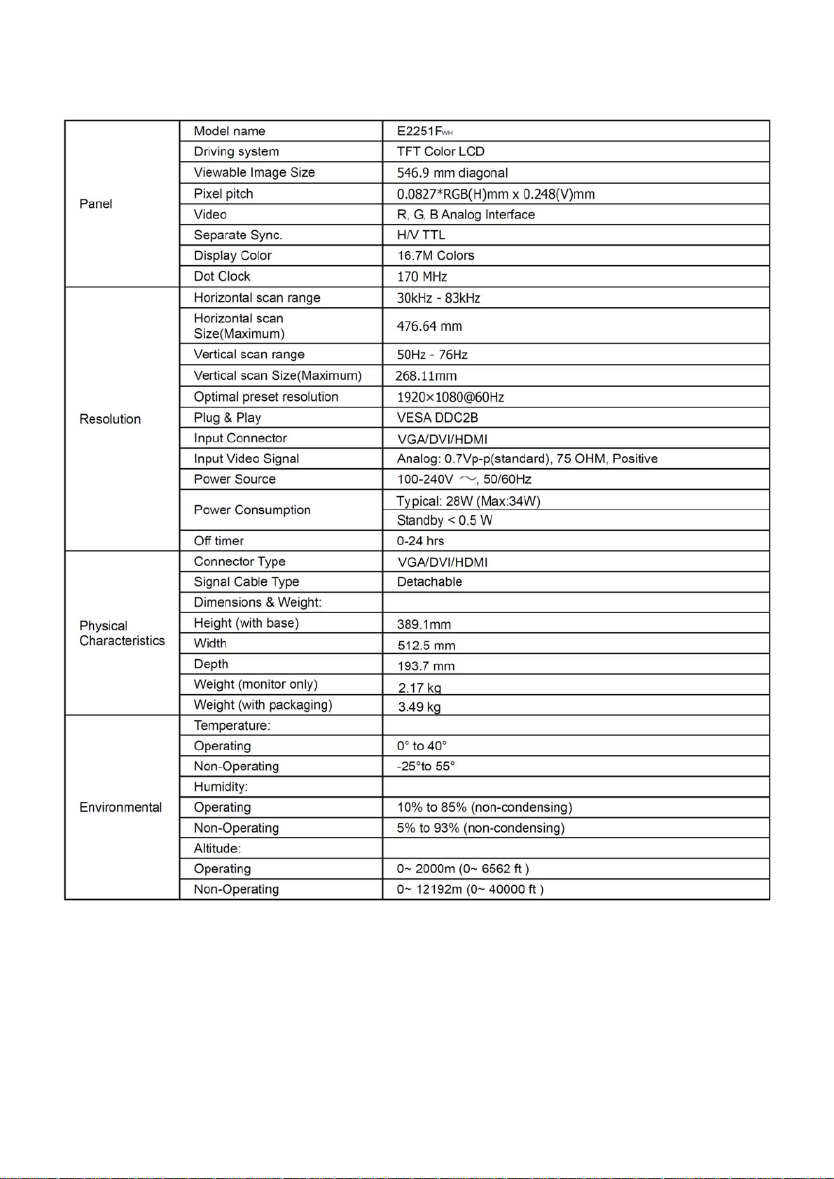
1. Monitor Specifications
4
Page 5
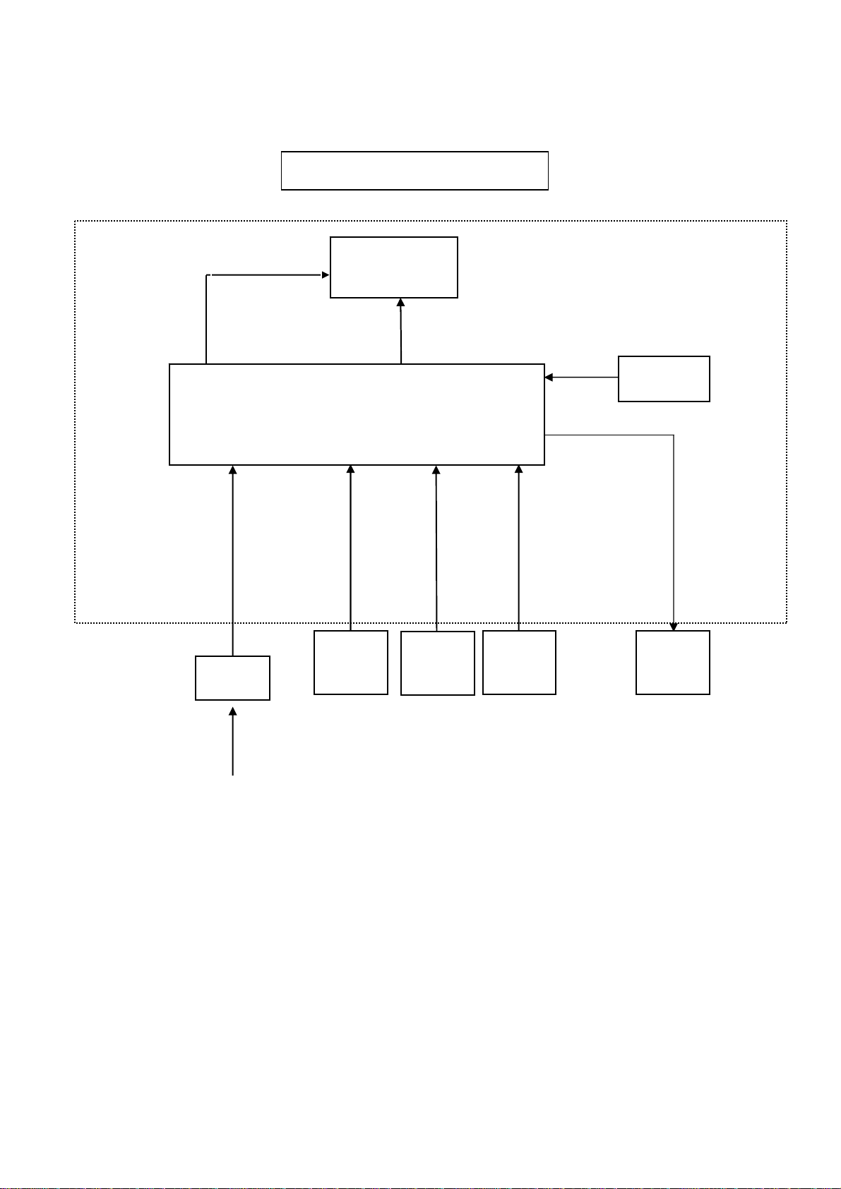
2. LCD Monitor Description
The LCD MONITOR will contain a main board and a key board which house the flat panel control logic, brightness
control logic and DDC.
Monitor Block Diagram
LED Drive.
Flat Panel and
LED backlight
Main Board
Key Board
Adapter
HDMI
Signal
DVI
Signal
D-SUB
Signal
Audio
out
AC-IN
100V~24
5
Page 6
3. Operating Instructions
3.1 General Instructions
Press the power button to turn the monitor on or off. The other control knobs are located at front panel of the monitor.
By changing these settings, the picture can be adjusted to your personal preferences.
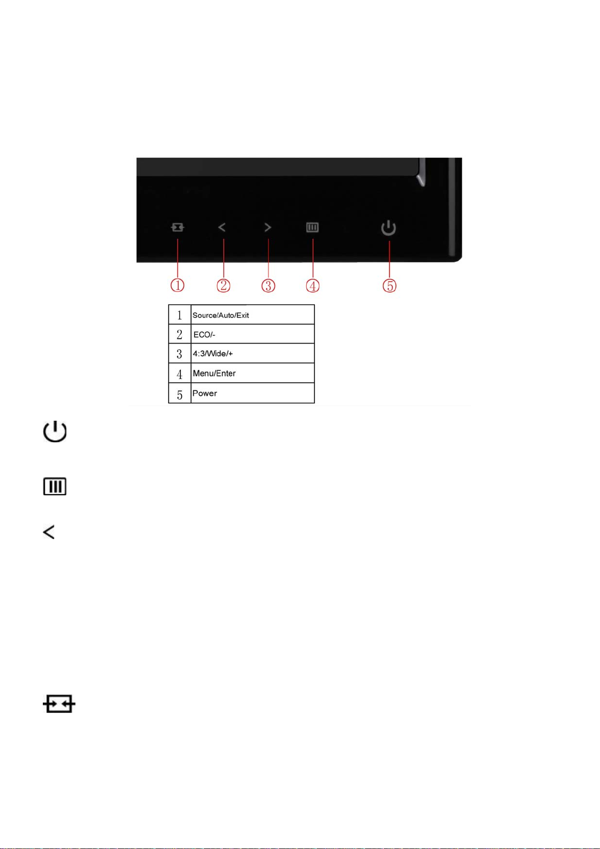
3.2 Hotkeys
Power
Press the Power button to turn on/off the monitor.
Menu/Enter
Press to display the OSD or confirm the selection
Eco (DCR)/-
Press the Eco key continuously to select the Eco mode of brightness and DCR on when there is no OSD. (Eco
mode hot key may not be available in all models).
4:3 or wide image ratio /Volume >
When there is no OSD and VGA input only, press hotkey continuously to change 4:3 or wide image ratio.
(If the product screen size is 4:3 or input signal resolution is wide format, the hot key is disable to adjust
and also only available for VGA input )
when HDMI input, press hotkey continuously to activate Volume, and press the Up or Down to change
the setting, press Menu button for confirmation and exit OSD. this only available for HDMI input
Source/Auto / Exit
When the OSD is closed, press Auto/Source/Exit button continuously about 2 second to do auto configure (only for
the models with dual or more inputs).
When the OSD is closed, press Auto/Source/Exit button will be Source hot key function (Only for the models with
dual or more inputs).
6
Page 7
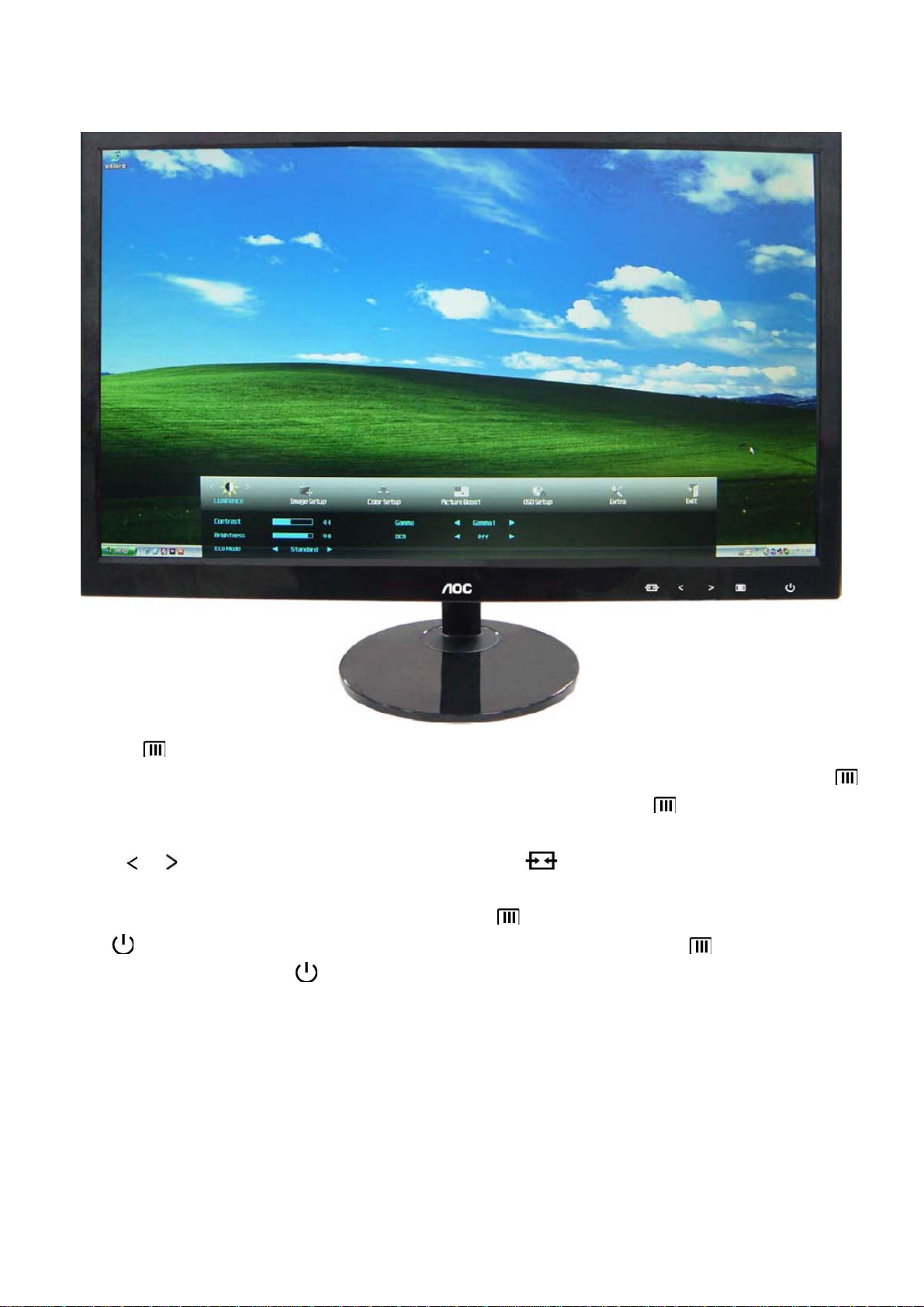
3.3 OSD Setting
Basic and simple instruction on the control keys.
1) Press the MENU-button to activate the OSD window.
2) Press < or > to navigate through the functions. Once the desired function is highlighted, press the
MENU-button to activate sub-menu . Once the desired function is highlighted, press
it.
Press or to change the settings of the selected function. Press AUTO to exit. If you want to
3)
adjust any other function, repeat steps 2-3.
4) OSD Lock Function: To lock the OSD, press and hold the MENU button while the monitor is off and then
press
the monitor is off and then press
Notes:
1) If the product has only one signal input, the item of "Input Select" is disable to adjust.
2) If the product screen size is 4:3 or input signal resolution is wide format, the item of "Image Ratio" is disable to
adjust.
3) One of DCR, Color Boost, and Picture Boost functions is active, the other two function is turned off accordingly.
power button to turn the monitor on. To un-lock the OSD - press and hold the MENU button while
power button to turn the monitor on.
MENU-button to activate
7
Page 8
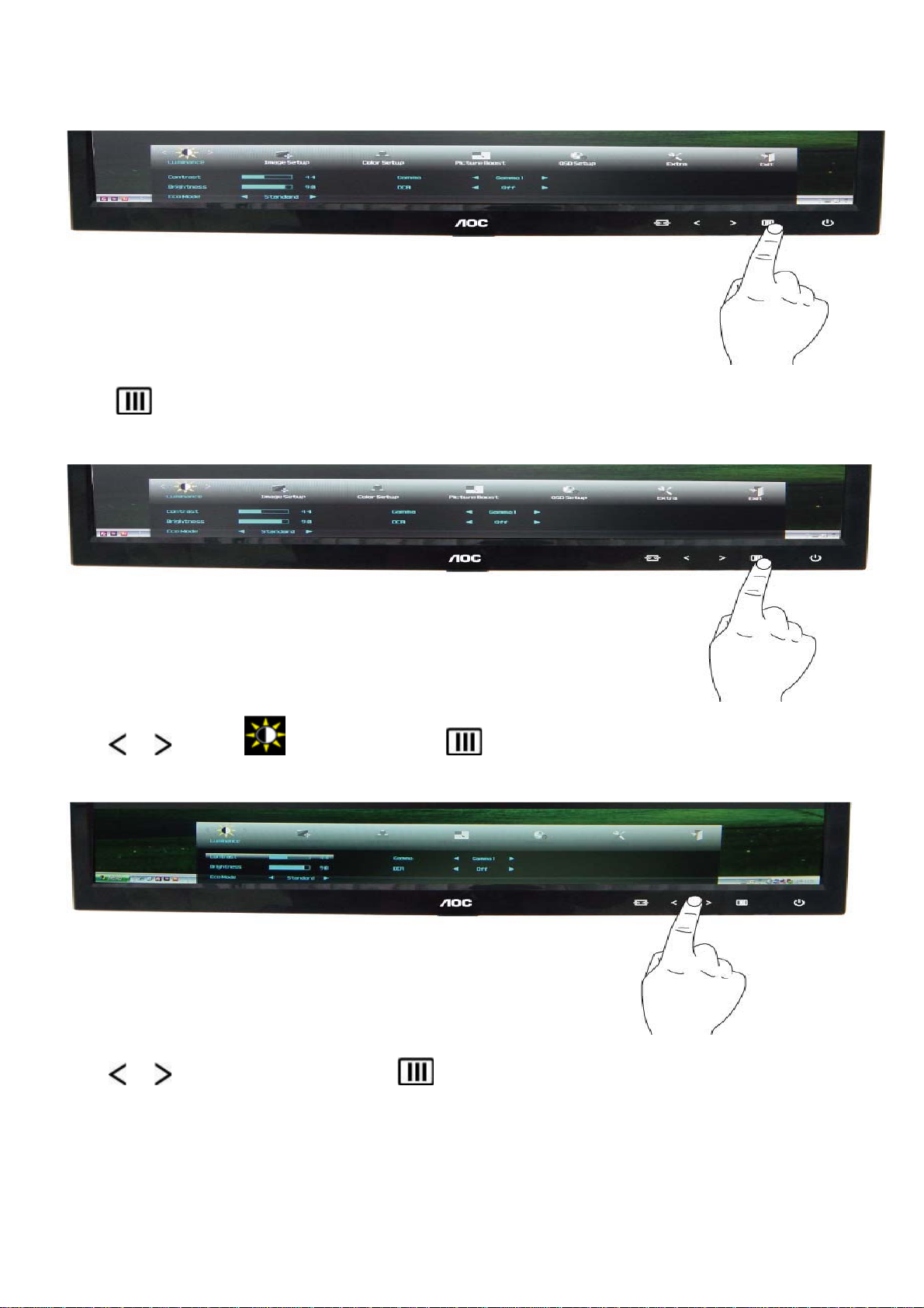
Luminance
1
Press
(Menu) to display menu
2
Press or to select (Luminance), and press to enter
3
Press or to select submenu, and press to enter.
8
Page 9
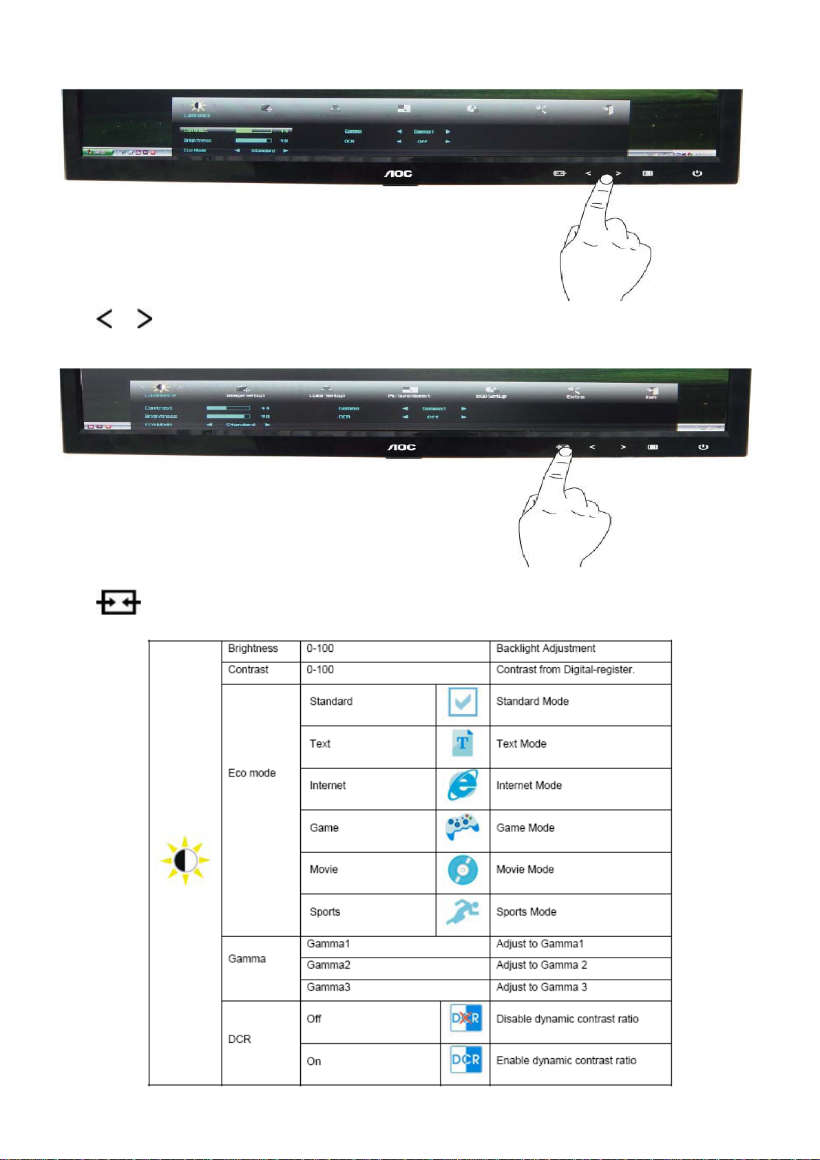
4
Press or to adjust
5
Press to exit.
9
Page 10
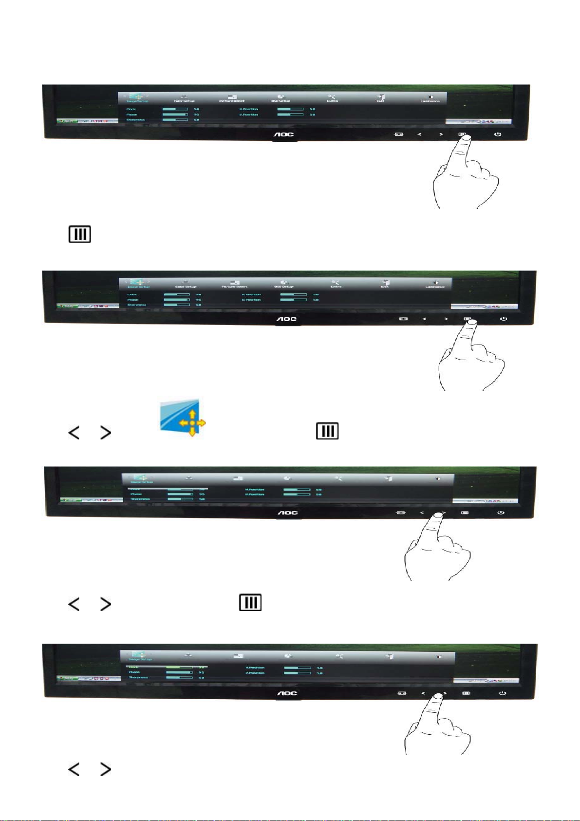
Image Setup
1
Press (Menu) to display menu
2
Press or to select (Image Setup) , and press to enter.
3
Press or to select submenu, and press to enter.
4
Press or to adjust.
10
Page 11
5
Press to exit.
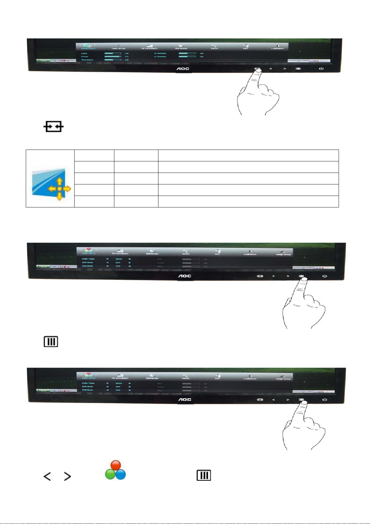
Color Setup
1
Clock 0-100 Adjust picture Clock to reduce Vertical-Line noise.
Phase 0-100 Adjust Picture Phase to reduce Horizontal-Line noise
Sharpness 0-100 Adjust picture sharpness
H.Position 0-100 Adjust the horizontal position of the picture.
V.Position 0-100 Adjust the vertical position of the picture.
Press (Menu) to display menu.
2
Press or to select (Color Setup), and press to enter.
11
Page 12
3
Press or to select submenu, and press to enter.
4
Press
or to adjust.
5
Press to exit.
12
Page 13
Warm Recall Warm Color Temperature from EEPROM.
Normal Recall Normal Color Temperature from EEPROM.
Cool Recall Cool Color Temperature from EEPROM.
Color setup.
DCB Mode
DCB Demo on or off Disable or Enable Demo
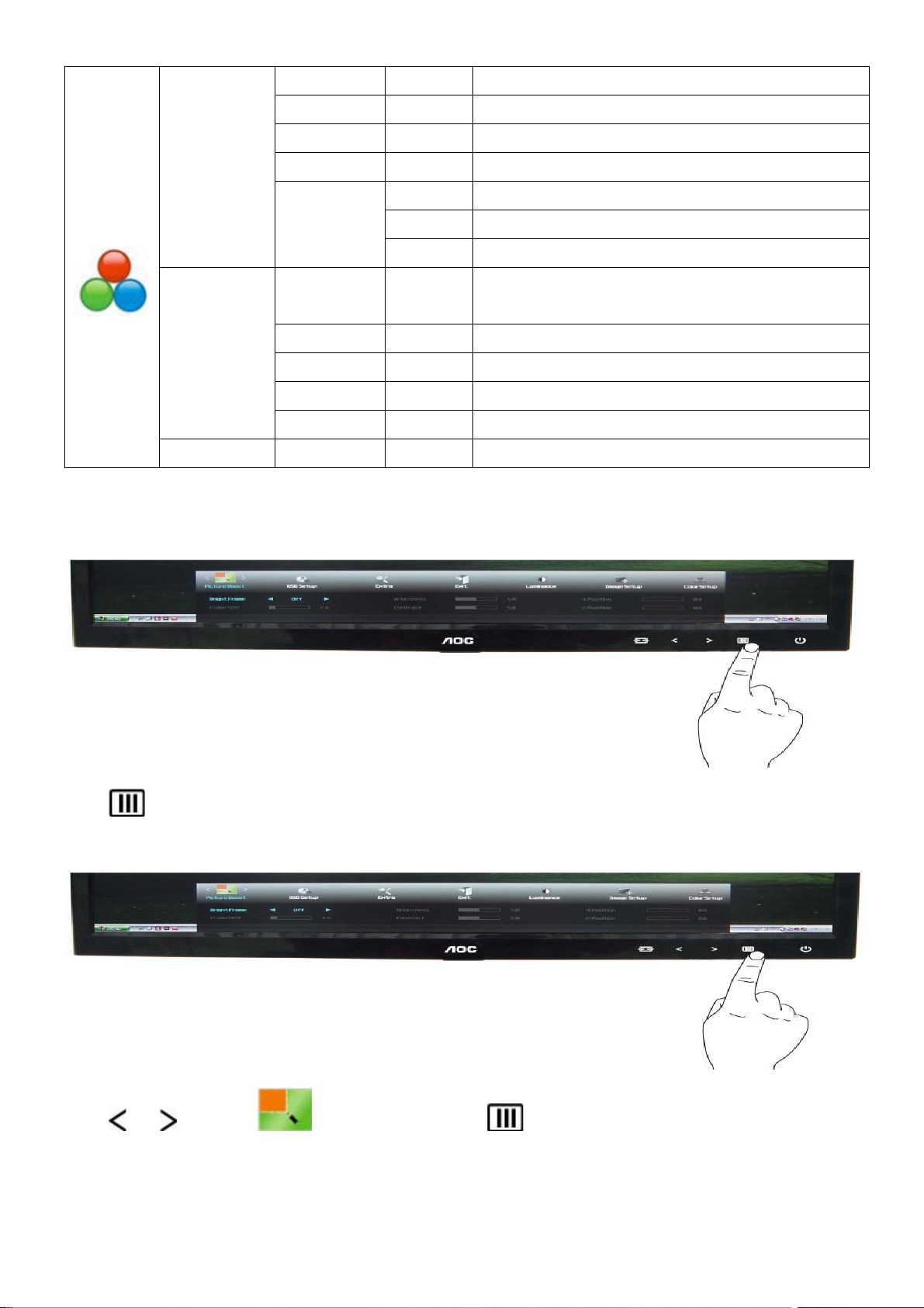
Picture Boost
1
sRGB Recall SRGB Color Temperature from EEPROM.
Red Red Gain from Digital-register
User
Green Green Gain Digital-register.
Blue Blue Gain from Digital-register
Full
on or off Disable or Enable Full Enhance Mode
Enhance
Nature Skin on or off Disable or Enable Nature Skin Mode
Green Field on or off Disable or Enable Green Field Mode
Sky-blue on or off Disable or Enable Sky-blue Mode
AutoDetect on or off Disable or Enable AutoDetect Mode
Press (Menu) to display menu.
2
Press or to select (Picture Boost), and press to enter.
13
Page 14
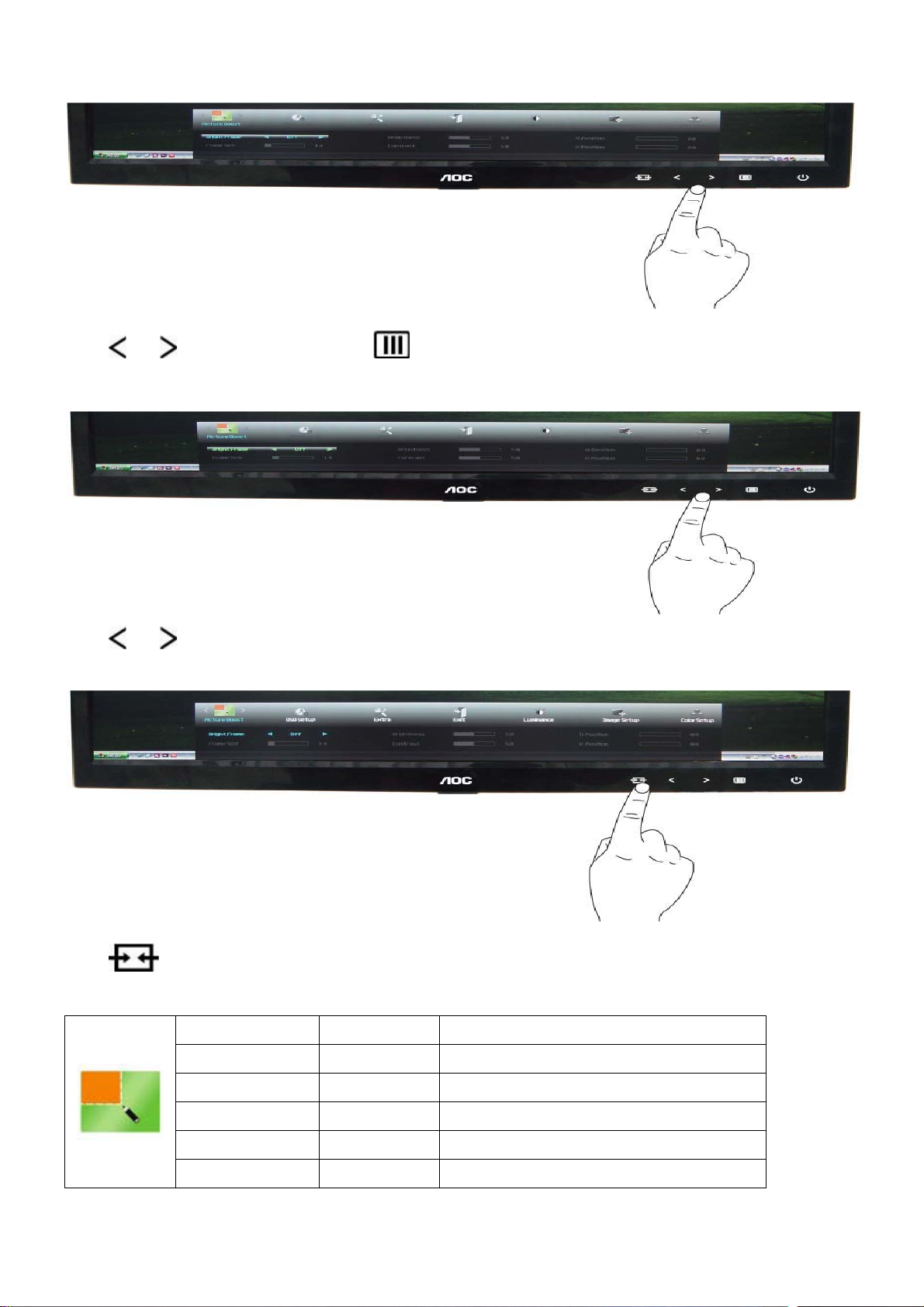
3
Press or to select submenu, and press to enter.
4
Press or to adjust.
5
Press to exit.
Frame Size 14-100 Adjust Frame Size
Brightness 0-100 Adjust Frame Brightness
Contras 0-100 Adjust Frame Contrast
H. position 0-100 Adjust Frame horizontal Position
V.position 0-100 Adjust Frame vertical Position
Bright Frame on or off Disable or Enable Bright Frame
14
Page 15
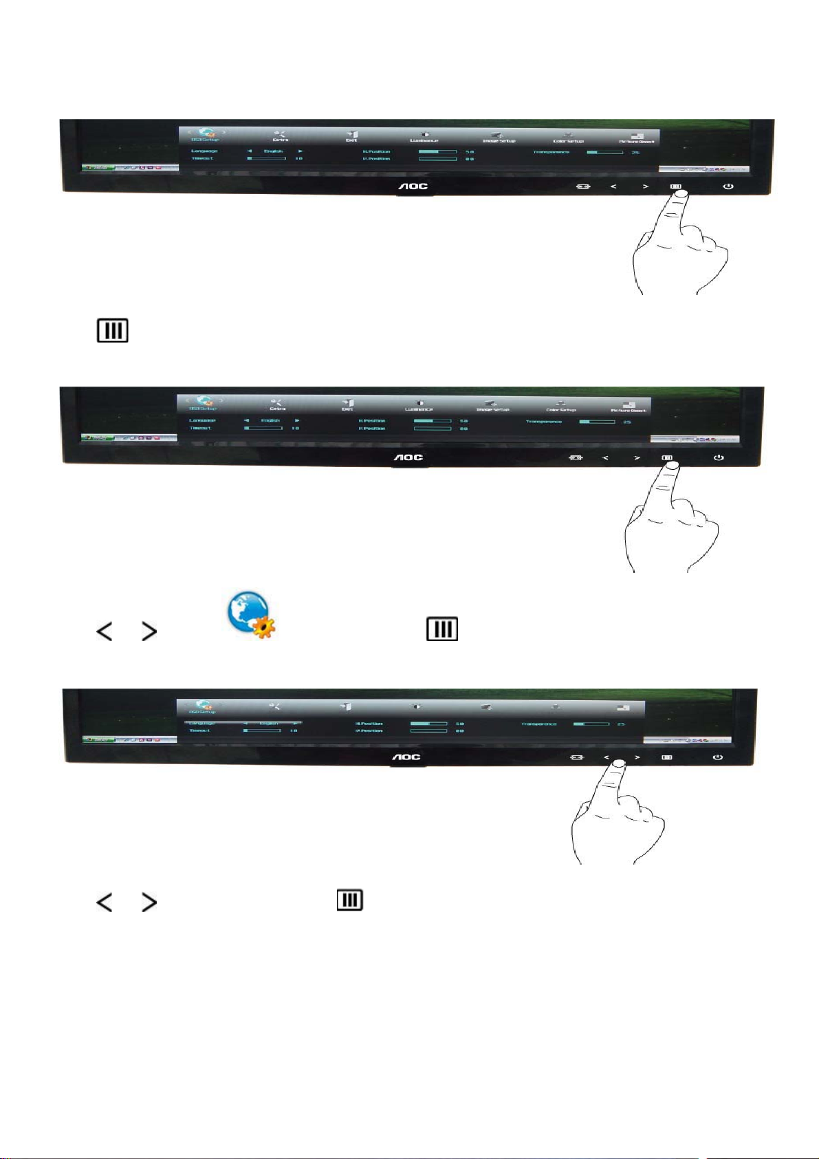
OSD Setup
1
Press (Menu) to display menu.
2
Press or to select (OSD Setup), and press to enter.
3
Press or to select submenu, and press to enter.
15
Page 16
4
Press or to adjust.
5
Press to exit.
H.Position 0-100 Adjust the horizontal position of OSD
V.Position 0-100 Adjust the vertical position of OSD
Timeout 5-120 Adjust the OSD Timeout
Transparence 0-100 Adjust the transparence of OSD
Language Select the OSD language
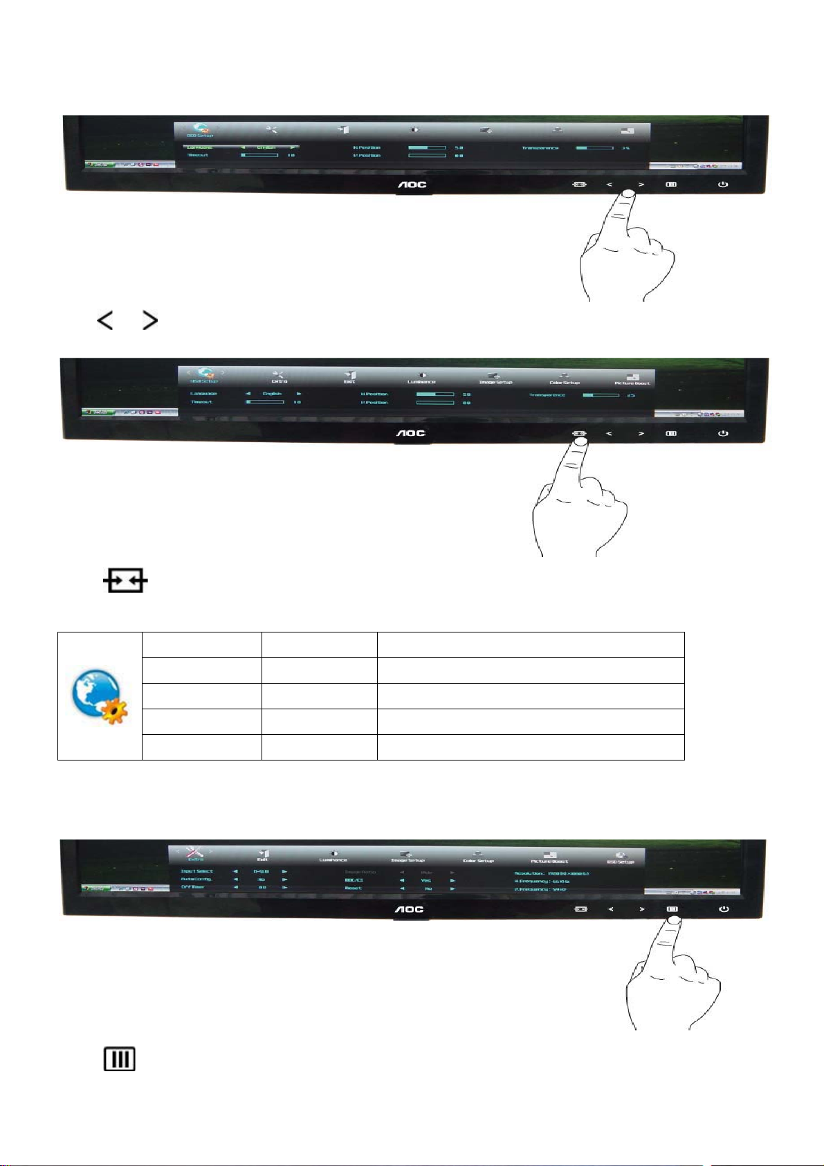
Extra
1
Press (Menu) to display menu.
16
Page 17

2
Press or to select (Extra), and press to enter.
3
Press or to select submenu, and press to enter.
4
Press or to adjust.
5
Press
to exit.
17
Page 18

Exit
1
Press (Menu) to display menu.
2
Press or to select (Exit), and press to exit.
Exit Exit the main OSD
18
Page 19

4. Input/Output Specification
4.1 D-SUB CONNECTORS and DVI CONNECTORS
Pin Assignments
Pin Number
1
2
3
15-Pin Side of the Signal Cable
Video-Red
Video-Green
Video-Blue
Pin Number 15-Pin Side of the Signal Cable
9 +5V
10
Ground
11 N.C.
4 N.C. 12 DDC- Serial data
5
Detect Cable
13 H-
sync
6 GND-R 14 V- sync
7 GND-G 15 DDC- Serial clock
8 GND-B
Pin Number 24-Pin Color Display Signal Cable Pin Number 24-Pin Color Display Signal Cable
1
TMDS
data 2-
13
TMDS
data 3+
2
TMDS
data 2+
3 TMDS data 2/4 Shield 15
4
5
TMDS
TMDS
data 4-
data 4+
6 DDC Clock 18
14
16
17
+5V Power
Ground(对于 +5V )
Hot Plug Detect
TMDS data 0-
TMDS
data 0+
7 DDC data 19 TMDS data 0/5 Shield
8 N.C. 20
9
10
TMDS
TMDS
data 1-
data 1+
21
22 TMDS
TMDS
TMDS data 5+
data 5-
Clock Shield
11 TMDS data 1/3 Shield 23 TMDS Clock +
12
TMDS
data 3-
24
TMDS Clock-
19
Page 20

4.2 Factory Preset Display Modes
20
Page 21

4.3 Panel Specification
4.3.1 General Features
BM215WF4-TJC1 is a Color Active Matrix Liquid Crystal Display with an integral Light Emitting Diode (LED)
backlight system. The matrix employs a-Si Thin Film Transistor as the active element. It is a transmissive type
display operating in the normally white mode. It has a 21.5 inch diagonally measured active display area with Full
HD resolution (1080 vertical by 1920 horizontal pixel array) Each pixel is divided into Red, Green and Blue
sub-pixels or dots which are arranged in vertical stripes. Gray scale or the brightness of the sub-pixel color is
determined with
a 8-bit gray scale signal for each dot, thus, presenting a palette of more than 16,7M colors with
Advanced-FRC(Frame Rate Control). It has been designed to apply the interface method that enables low power,
high speed, low EMI. FPD Link or compatible must be used as a LVDS(Low Voltage Differential Signaling) chip. It is
intended to support applications where thin thickness, wide viewing angle, low power are critical factors and graphic
displays are important. In combination with the vertical arrangement of the sub-pixels, the BM215WF4-TJC1
characteristics provide an excellent flat panel display for office automation products such as monitors.
4.3.2 Display Characteristics
21
Page 22

4.3.3 Electrical Characteristics
Parameter Symbol
MODULE :
Values
Unit Notes
Min Typ Max
Power Supply Input Voltage V
Permissive Power Input Ripple V
Power Supply Input Current
Power Consumption P
Inrush current I
LED bar Electrical characteristics
Parameter Symbol Condition
4.5 5.0 5.5 Vdc
LCD
- - 0.3 V 3
LCD
I
LCD-MOSAIC
I
LCD-BLACK
I
LCD-BLACK
LCD
RUSH
(60Hz) - 1000 1300 mA 1,5
(60Hz) - 1300 1690 mA 2,5
(75Hz) - 2000 mA 5
- 5.00 6.5 Watt 1
- - 3.0 A 1, 4
Values
Unit Notes
Min. Typ. Max.
LED : 1,7
LED String Current Is - 110 120 mA 2,7
LED String Voltage Vs 48.0 51.2 54.4 V 3,7
Power Consumption PBar - 11.3 12.0 Watt 4,6,7
LED Life Time LED_LT 30,000 - - Hrs 5,7
22
Page 23

4.3.4 Optical Characteristics
Ta=25 °C, V
=5.0V, fV=60Hz, D
LCD
Values
Parameter Symbol
Min Typ Max
Contrast Ratio CR 700 1000 -
Surface Luminance, white LWH 200 250 - cd/m2
Luminance Variation
Rise Time Tr
WHITE
9P 75 - - %
- 1.3 2.6 ms
R
Response Time
Decay Time TrD - 3.7 7.4 ms
Rx
0.642
RED
Ry 0.332
Gx 0.305
GREEN
Color Coordinates
[CIE1931]
Gy 0.625
Bx 0.150
Typ
-0.03
Typ
+0.03
BLUE
By 0.068
=72MHz, Is=110mA
CLK
Units Notes
1
(PR-880)
2
(PR-880)
3
(PR-880)
4
(RD80S)
(PR-650)
WHITE
Viewing Angle (CR>5)
x axis, right(=0°) r
x axis, left (=180°) l
y axis, up (=90°) u
y axis, down (=270°) d
Viewing Angle (CR>10)
x axis, right(=0°) r
x axis, left (=180°) l
y axis, up (=90°) u
y axis, down (=270°) d
Crosstalk
Wx 0.313
Wy 0.329
75 88
75 88
Degree
70 85
70 85
70 85
70 85
Degree
60 75
70 85
1.5 %
5
(PR-880)
6
(PR880)
Luminance uniformity -
LR - - 1.7
Angular dependence (TCO’03)
Color grayscale linearity Δu’v’ 0.018 9 (PR-650)
23
7
(PR880)
Page 24

5. Block Diagram
5.1 Main Board
Flash Memory
MX25L2026DM1I-1
2G (U402)
CRYSTAL
14.318MHZ
(X401)
D-Sub Connector
(CN101)
Panel Interface
(CN406)
Scalar IC NT68677UMFG/E
(Include ADC, OSD, MCU)
(U401)
DVI Connector
(CN102)
Key Control Interface
(CN405)
Audio decoder
APA2176A (U601)
HDMI Connector
PHONE JACK
(CN501)
(CN603)
LED
(CN803)
D801
Feedback Circuit
L801
MOSFET
(Q806)
PWM Control
MP3389EF
(U801)
12V
ON/OFF
DIM
24
Page 25

6. Schematic
6.1 Main Board
715G4810M01BRA004L
CN101
1716
D-SUB 15P
1
11
12
13
14
15
HSI
VSI
CN102JACK
VSYN C
SYN C GND
DDC SCL
DDC SDA
HPD
1/3shie ld
2/4shie ld
0/5shie ld
clk shield
DAT0+
DAT0-
DAT1+
DAT1-
DAT2+
DAT2-
DAT3+
DAT3-
DAT4+
DAT4-
DAT5+
DAT5-
GND26GND25GND28GND
27
+5V
clk+
clk-
RED+
6
RED-
2
GREEN+
7
GREEN-
3
BLUE+
8
BLUE-
4
9
VGA5V
5
10
ZD101
RLZ5.6B
8
15
6
SCL_DVI
7
SDA_DVI
14
16
HPD
11
3
19
22
18
DAT0+
17
DAT0-
10
DAT1+
9
DAT1-
2
DAT2+
1
DAT2-
13
12
5
4
21
20
23
DCLK+
24
DCLK-
R111 0R05 1/10W
R114
2K2 1/16W 5%
DET_DVI
U104
1
I/O1
2
GND
I/O23I/O3
AZC399-04S
1
2
DET_DVI
I/O4
VDD
1
2
U101
I/O1
I/O4
GND
VDD
I/O23I/O3
AZC399-04S
6
5
4
U106
I/O1
I/O4
GND
VDD
I/O23I/O3
AZC399-04S
DET_VGA
C111
22pF 50V
6
5
4
6
5
4
C125
100N16V
FB101
19 OHM 500mA
1 2
FB102
19 OHM 500mA
1 2
FB103
19 OHM 500mA
1 2
C105
C101
5PF 50V
ESD_VGA
C110
100N 16V
R115
2K2 1/16W 5%
ADC4
R127 47R 1/16W 5%
R128 47R 1/16W 5%
1 2
ESD_DVI Q101
DET_DVII 5
FB105300OHM
U107
1
I/O1
I/O4
2
GND
VDD
I/O23I/O3
AZC399-04S
R110 100R 1/16W 5%
R112 100R 1/16W 5%
R113 100R 1/16W 5%
C112
22pF 50V
NC/22P 50V
SCL_VGA
SDA_VGA
DVI5V1
ZD102
NC/ RLZ5.6B
6
ESD_DVI
5
4
C126
100N16V
C106
5PF 50V
5PF 50V
C113
R129 1K 1/16W 5%
C128
NC/100N16V
R135 10R 1/16W 5%
R136 10R 1/16W 5%
R137 10R 1/16W 5%
R138 10R 1/16W 5%
R139 10R 1/16W 5%
R140 10R 1/16W 5%
R141 10R 1/16W 5%
R142 10R 1/16W 5%
R101
75 OHM +-5% 1/ 16W
CMVCC13,4,5, 6,7
DET_VGA1 5
C114
NC/22P 50V
R119 47R 1/16W 5%
R120 47R 1/16W 5%
R130 NC
NC
R105
R106
75 OHM +-5% 1/ 16W
75 OHM +-5% 1/ 16W
HSYNC 5
VSYN C 5
DDCA_SDA5
DDCA_SCL5
R143
NC
RX0+ 5
RX0- 5
RX1+ 5
RX1- 5
RX2+ 5
RX2- 5
RXC+ 5
RXC- 5
CMVCC1
PE0*
R102 10R 1/16W 5%
R103 10R 1/16W 5%
R104 10R 1/16W 5%
R107 47R 1/16W 5%
R108 47R 1/16W 5%
R109 47R 1/16W 5%
R116
R117
4K7 1/16W 5%
4K7 1/16W 5%
DVI_HPD 5
絬 隔 瓜 絪 腹
Key Component
C102 47N16V
C103 47N16V
C104 47N16V
C107 47N16V
C108 47N16V
C109 47N16V
VGA5V
1
2
D103
BAV70
3
U102
GND
FM24C02A
DDC_WP
A0
A1
A2
1
2
3
4
DDC_WP 3,5
DVI_SDA5
DVI_SCL5
8
R118
22K 1/16W 5%
T P V ( Top Victory Electronics Co . , Ltd. )
Date
VCC
7
WP
6
SCL
5
SDA
G4810-M0C-AOC-X--1-110315
2.0.I NPUT
RIN 5
GIN 5
BIN 5
GNDR 5
GNDG 5
GNDB 5
VSI
HSI
R148 1K 1/16W 5%
C115
220N16V
R132 4K7 1/16W 5%
OEM MO DEL
TPV MODEL
PCB NAME
Sheet
BLUE+
GREEN+
RED+
C117
C118
C119
NC/5PF 50V
NC/5PF 50V
NC/5PF 50V
U103
1
2
R133 4K7 1/16W 5%
I/O1
GND
I/O23I/O3
AZC399-04S
R134 22K 1/16W 5%
AOC
e2351Fh
28Monday, April 18, 2011
6
SCL_VGA
I/O4
5
VDD
4
SDA_VGA
ESD_VGA
DVI5V1
CMVCC1
1
2
D102
BAV70
3
of
ESD_VGA
C116
100N 16V
FB104
R149
1K 1/16W 5%
Custom
A
<
称爹
DVI5V 5
ESD_DVI
>
120 OHM
C145
1N 50V
C127
220N16V
U105
GND
FM24C02A
PC4
A0
A1
A2
DDC_WP
1
2
3
4
Size
Rev
称爹
8
VCC
7
WP
6
SCL
5
SDA
25
Page 26

CN501
HDMI
20
TH1
21
TH2
22
TH3
23
TH4
24
TH5
HDMI1_HOTPLUG
HDMI1_D ET
D2 Shield
D1 Shield
D0 Shield
CK Shield
CE Remote
DDC CLK
DDC DATA
GND
HP DET
D2+
D2-
D1+
D1-
D0+
D0-
CK+
CK-
NC
+5V
1
2
I/O1
GND
I/O23I/O3
1
2
3
4
5
6
7
8
9
10
11
12
13
14
15
16
17
18
19
100N 16V
U505
I/O4
VDD
AZC399-04S
300OHM
C505
ESD_HD MI1
6
5
4
HDMI1_DET
R527 N C
FB501
HDMI1_+5V
1 2
R529
1K 1/16W 5%
HDMI1_HOTPLUG
HDMI1_SC L_A
HDMI1_SDA_A HDMI1/CK+
C506
100N 16V
R533 10R 1/16W 5%
HDMI1_+5V
ZD503
RLZ5.6B
HDMI1/CK-
HDMI1/D0HDMI1/D0+
HDMI1_SC L_A
HDMI1_SDA_A
U506
TVU1240R1A
10
NC
9
NC
7
NC
6
NC
HDMI1_+5V 5
HDMI1_HPD 5
IN1
IN2
IN3
IN4
GND
GND
3
8
HDMI1/D2+
HDMI1/D2HDMI1/D1+
HDMI1/D1HDMI1/D0+
HDMI1/D0HDMI1/CK+
HDMI1/CKCEC_CTRL_A
1
HDMI1/CK-
2
HDMI1/CK+
4
5
HDMI1/D0HDMI1/D0+
ZD502
NC/RLZ5.6B
HDMI1_SC L_A
HDMI1_SD A_A
HDMI1_SDA5
HDMI1_SCL5
R528 N C
R534 47R 1 /16W 5%
R535 47R 1 /16W 5%
HDMI1/D1+
HDMI1/D2HDMI1/D2+
U507
TVU1240R1A
10
NC
9
NC
7
NC
6
NC
R518 0R 05 1/16W
R519 0R 05 1/16W
R520 0R 05 1/16W
R521 0R 05 1/16W
R522 0R 05 1/16W
R523 0R 05 1/16W
R524 0R 05 1/16W
VCC
WP
SCL
SDA
FM24C02A
R526 0R 05 1/16W
U508
1
A0
2
A1
3
A2
4
GND
CEC_CTRL
R532
8
22K 1/16W 5%
7
6
5
DDC_WP 2,5
R531
R530
4K7 1/16W 5%
4K7 1/16W 5%
DDC_WP
1
IN1
IN2
IN3
IN4
GND
GND
3
8
HDMI1/D1-HDMI1/D1-
2
HDMI1/D1+
4
HDMI1/D2-
5
HDMI1/D2+
C504
220N16V
HDMI1_D 2+ 5
HDMI1_D 2- 5
HDMI1_D 1+ 5
HDMI1_D 1- 5
HDMI1_D 0+ 5
HDMI1_D 0- 5
HDMI1_CK+ 5
HDMI1_CK- 5
CEC_CTRL 5
HDMI1_+5V
D502
BAT54C
CMVCC1
CMVCC1 2,4,5,6,7
ESD_HD MI1
R539 1K 1/ 16W 5%
HDMI1_DET
R538
NC/ 10K 1/16W 5%
R537
NC/ 10K 1/16W 5%
R536 100R 1/16W 5%
Q501
NC/ LMBT3904LT1G
DET_HDMI1 5
26
T P V ( Top Victory Electronics Co . , Ltd. )
絬 隔 瓜 絪 腹
Key Component
G4810-M0C-AOC-X--1-110315
3.0HD MI
Date
OEM MO DEL
TPV MODEL
PCB NAME
Sheet
AOC
e2351Fh A
of
38Monday, April 18, 2011
Size
Rev
称爹
称爹
<
Custom
>
Page 27

RXO0RXO1RXO2RXOCRXO3RXE0RXE1RXE2RXECRXE3SDA_PANEL
PA[0.. 9]
2
4
6
8
10
12
14
16
18
20
22
24
26
28
30
CN407
NC/CONN
PA0 LVA3P
PA1 LVA3M
PA2 LVACKP
PA3 LVACKM
PA4 LVA2P
PA5 LVA2M
PA6 LVA1P
PA7 LVA1M
PA8 LVA0P
PA9 LVA0M
1
3
5
7
9
11
13
15
17
19
21
23
25
27
29
PB[0..9]5PA[0.. 9]5
RXO0+
RXO1+
RXO2+
RXOC+
RXO3+
RXE0+
RXE1+
RXE2+
RXEC+
RXE3+
SCL_PANEL
PB[0.. 9]
PANEL_VCC
C141
100UF 16V
1 2
+
FB108
120 OHM
LVB3PPB0
LVB3MPB1
LVBCKPPB2
LVBCKMPB3
LVB2PPB4
LVB2MPB5
LVB1PPB6
LVB1MPB7
LVB0PPB8
LVB0MPB9
PANEL_VCC
R146300 OHM 1/4W
R147300 OHM 1/4W
C142
100N 16V
RXO0-LVB0M
RXO0+LVB0P
RXO1-LVB1M
RXO1+LVB1P
LVB2M RXO2-
RXO2+LVB2P
LVBCKM RXOC-
RXOC+LVBCKP
RXO3-LVB3M
RXO3+LVB3P
RXE0-LVA0M
LVA0P RXE0+
RXE1-LVA1M
RXE1+LVA1P
RXE2-LVA2M
RXE2+LVA2P
LVACKM RXEC-
RXEC+LVAC KP
RXE3-LVA3M
RXE3+LVA3P
CONN
30
29
28
27
26
25
24
23
22
21
20
19
18
17
16
15
14
13
12
11
10
9
8
7
6
5
4
3
2
1
CN406
RXEC-
C143
NC
RXEC+
CMVCC1
CMVCC12,3,5,6,7
R305
10K 1/16W 5%
PPWR_ON #5
R303
4K7 1/16W 5%
R304
22K 1/16W 5%
C304
100N 16V
Q302
LMBT3904LT1G
RXOC-
C144
NC
RXOC+
R306
100K 1/16W 5%
R307
NC
3
D
12
S
G
PANEL_VCC
C303
220N16V
Q301
AO3401A
SDA_PAN EL
SCL_PANEL
5
U301
D8D7D6D
NC/AO4411
S1S2S3G
4
CMVCC1
SDA_PANEL 5
SCL_PAN EL 5
AO3401L
T P V ( Top Victory Electronics Co . , Ltd. )
絬 隔 瓜 絪 腹
Key Component
G4810-M0C-AOC-X--1-110315
4.0.OU TPUT
Date
OEM MODEL
TPV MO DE L
PCB NAME
AOC B
e2351Fh
48Sat urday , J une 25, 2011
Sheet
of
Size
Rev
称爹
A
<
称爹
>
27
Page 28

C424
220N16V
C426
100N 16V
VCC3.3
R422
10K 1/16W 5%
VCC3.3
R420
NC
WP
R421
10K 1/16W 5%
C427 47pF 50V
C428 47pF 50V
DVI_VCC
HDMI1_SCL3
HDMI1_SDA3
DVI_SCL2
DVI_SDA2
DDCA_SCL2
DDCA_SDA2
1
2
3
MX25L2026DM1I-12G
HDMI1_D0-3
HDMI1_D0+3
HDMI1_D1-3
HDMI1_D1+3
HDMI1_D2-3
HDMI1_D2+3
HDMI1_CK-3
HDMI1_CK+3
RX0-2
RX0+2
RX1-2
RX1+2
RX2-2
RX2+2
RXC-2
RXC+2
U402
CS
SO
WP
GND4SI
1 2
X401
12MHz
R401
470R 1%
BIN2
GNDB2
GIN2
GNDG2
RIN2
GNDR2
HSYNC2
VSYNC2
8
VCC
7
HOLD
6
SCK
5
WP
R424 1MOHM 1/16W +/-5%
R425 0R05 1/16W
LED_GRN/BLUE
MVDD
RSTB
OSCI
OSCO
1
126
7
8
12
13
17
18
2
3
122
123
9
10
14
15
19
20
4
5
124
125
22
23
24
25
26
27
36
37
41
42
30
31
32
33
34
35
38
39
43
44
70
69
72
71
73
114
116
117
REXT
MVDD
RX10RX10+
RX11RX11+
RX12RX12+
RX1CRX1C+
PA4*/DD C_SCL2*
PA5*/DD C_SDA2*
RX20RX20+
RX21RX21+
RX22RX22+
RX2CRX2C+
PA6*/DD C_SCL3*
PA7*/DD C_SDA3*
BIN1+
BIN1GIN1+
GIN1RIN1+
RIN1HSYNCI2
VSYNC I2
PB4*/DD C_SCL0*
PB5*/DD C_SDA0*
BIN0+
BIN0GIN0+
GIN0RIN0+
RIN0HSYNCI1
VSYNCI1/TOUTP
PB6*/DD C_SCL1*
PB7*/DD C_SDA1*
SPI_SO
SPI_CE
SPI_CK
SPI_SI
PD4/AMUTE
RSTB
OSCI
OSCO
R445
2K2 1/16W 5%
NC/100R 1/ 10W 5%
DVI_VCC
R460
ADC_VDD
16
128
AVCC
AVCC
AGND
AGND
ADC_GNDA
6
11
21
A_VCC
DVDD
29
53
87
66
104
DVDD
DVDD
DVDD
ADC_VDD
U401
NT68677UMFG/E
DGND
DGND
40
98
76
R444 0R05 1/16W
Q402
LMBT3906LT1G
R446
200R 1/10W 5%
CVDD
118
DVDD
OSC_VDD
DGND
DGND
127
115
VCC3.3
ADC_1V8
52
99
CVDD
DGND
CMVCC1
119
CVDD
CVDD
AUDIO_VDD
MVDD
28
65
54
MVDD
ADC_1V8
AUDIO_VDD
PC6/PWM10/SPDIF
PC3*/PWM7*/CEC3*
PC1*/PWM5*/ LPD_OUT*
PC0*/PWM4*/CEC2*
P31*/TXD*/SPDIF*
PA3*/PWM3*/ ADC7
PA2*/PWM2*/ ADC6
PA1*/PWM1*/ ADC5
PA0*/PWM0*/ ADC4/D BC2*
PB3/ADC3/ INTE3
PB2/ADC2/ INTE2
PB1/ADC1/ INTE1
PB0/ADC0/ INTE0
PE2*/PWMA*/ DBC0*
PE3*/PWMB*/ DBC1*
AUDIO_BY PASS
AUDIO_GND
DGND
55
64
CMVCC1 2,3,4, 6,7
TCLK1M
TCLK1P
TCLK2M
TCLK2P
PC7/PWM11
PC5/PWM9
PC4/PWM8
PC2*/PW M6*
P30*/RXD*
PE1*/LPD_I N1*
PE0*/LPD_I N0*
MCLK/ AOU T_L
SCK/AOUT_R
I2S0/AIN0_L
I2S1/AIN0_R
I2S2/AIN1_L
I2S3/AIN1_R
T0M
T0P
T1M
T1P
T2M
T2P
T3M
T3P
T4M
T4P
T5M
T5P
T6M
T6P
T7M
T7P
PD6
PD5
P35*
P34*
WD
97
96
95
94
93
92
91
90
89
88
86
85
84
83
82
81
80
79
78
77
75
R462 47R 1/16W 5%
74
R463 47R 1/16W 5%
109
R469 10K 1/16W 5%
103
R468 4K7 1/16W 5%
108
102
107
101
106
100
68
DET_DVI5V
67
DET_HDMI1_+5V
46
45
121
120
113
R413 100R 1/16W 5%
112
R414 100R 1/16W 5%
111
R415 100R 1/16W 5%
110
50
5V_DET
49
R417 100R 1/16W 5%
48
47
51
105
63
62
61
60
59
58
57
56
C425
10uF 10V
R451
4K7 1/16W 5%
LED_ORAN GE
R461
NC/100R 1/ 10W 5%
DET_DVII
DET_HDMI1
PB9
PB[0..9]
PB8
PB7
PB6
PB5
PB4
PB3
PB2
PB1
PB0
PA9
PA[0..9]
PA8
PA7
PA6
PA5
PA4
PA3
PA2
PA1
PA0
20091218-MODIFY
adj_BACKLIGHT
R448 0R05 1/16WR443 NC
R450 NC /0R05 1/16W
Q404
LMBT3906LT1G
DVDD
R402
100K 1/16W 5%
PB[0..9] 4
PA[0..9] 4
R405 4K7 1/16W 5%
R406 4K7 1/16W 5%
R455
0R05 1/10W
CHANGE 100R
DET_DVII
DET_HDMI1
DVI_HPD
HDMI1_HPD
DDC_WP
LINE_OUTR 7
LED_RLED_G
SDA_PANEL 4
SCL_PANEL 4
POWER_KEY #
KEY2
KEY1
adj_BACKLIGHT 6
LINE_OUTL 7
VCC3.3
CMVCC1
R403
100K 1/16W 5%
DET_DVII 2
DET_HDMI1 3
LED_GRN/BLUE
LED_ORANGE
on_BACKLIGHT 6
PPWR_ON# 4
DDC_WP 2,3
AUDIO_MUTE 7
VCC3.3
1 2
DVDD
R409 NC
R410 NC
NC/CONN
FB403
120 OHM
C411
100N 16V
DVI_HPD 2
HDMI1_HPD 3
DVDD
CN401
CN404
NC/CONN
ADC_VDD
DVDD
R416
100K 1/16W 5%
1
2
3
4
5
6
7
8
7
6
5
4
3
2
1
CN403
NC/CONN
CN402
NC/CONN
VCC3.3
DET_VGA1 2
1
2
3
4
5
6
7
6
5
4
3
2
1
FB401
1 2
120 OHM
10uF 10V
C412
10uF 10V
DVI_VCC
C402
CONN
VCC3.3
CN405
DVI_VCC
1 2
2
1
2
3
4
5
6
C403
100N 16V
FB404
120 OHM
100N 16V
D401
NC
3
C404
100N 16V
A_VCC
C413
1
R423
NC
CMVCC1
R404
100K 1/16W 5%
R407
200K
C414
10uF 10V
VCC1.8
CEC_CTRL 3
5V_DET
/0.68027
5V/0.68027=3.401V
4.5V/0.68027=3.061V
R440 NC
R441 NC
R452 0R05 1/16W
R453 0R05 1/16W
TOUCH_POWER
VCC3.36,7
VCC3.3
FB407
1 2
120 OHM
C420
10uF 10V
DVI5V2
D404 NC/R LZ5.6B
FB405
1 2
120 OHM
C415
100N 16V
VCC1.8 6
CVDD
DET_DVI5V
/0.68027
VCC3.3
1 2
VCC3.3
AUDIO_VD D
100N 16V
C421
100N 16V
KEY1
KEY2
POWER_KEY #
LED_G
LED_R
FB411
NC/120 OHM
C442
NC/100N 16V
FB402
1 2
120 OHM
C405
10uF 10V
C416
10uF 10V
C422
C423
100N 16V
DVI5V
R411
NC/100K 1/16W 5%
R418
NC/200K
R465
NC/3K9 +/-5% 1/16W
C437 100N 16V
C438 100N 16V
1 2
DVDD
C406
100N 16V
VCC3.3
VCC1.8
1 2
NC/3K9 +/-5% 1/16W
C439 NC/100N 16V
1 2
LED_R
FB412
NC/120 OHM
C407
100N 16V
1 2
FB406
120 OHM
C418
100N 16V
HDMI1_+5V3
R466
D402 RLZ5.6B
C408
100N 16V
FB410
120 OHM
C436
10uF 10V
ADC_1V8
DET_HDMI1_+5V
/0.68027
VCC3.3
C440 NC/100N 16V
1 2
C409
100N 16V
MVDD
C401
100N 16V
C419
10uF 10V
HDMI1_+5V
R467
NC/3K9 +/-5% 1/ 16W
D403 RLZ5.6B
C441 NC/100N 16V
1 2
C410
100N 16V
R412
NC/100K 1/16W 5%
R419
NC/200K 1/16W 5%
D405 RLZ5.6B
28
Aug-08-24 change value 0 to 4.7K
T P V ( Top Victory Electronics Co . , Ltd. )
G4810-M0C-AOC-X--1-110315
絬 隔 瓜 絪 腹
Key Component
5.0.SCALER
Date
OEM MOD EL Size
AOC
TPV MOD EL
e2351Fh
PCB NAME
58Monday, April 18, 2011
of
Sheet
C
Rev
A
<
称爹
>
称爹
Page 29

U706
2
VIN3VOUT
U701
U704
VI3VO
1
U702
VI3VO
1
GND
1
ADJ(GND)1VOUT(TAB)2VIN
GND
2
GND
3
C709
100N 16V
VCC3.3
+
C707
100UF 16V
2
CMVCC1
12
D707
SR34
12
D708
SR34
CMVCC1
R702
10K 1/16W 5%
BKLT-EN8
BKLT-EN
C702
100N 16V
Q701
LMBT3904LT1G
CMVCC1
R704 22K 1/ 16W 5%
R703
10K 1/16W 5%
on_BACKLIGHT 5
VCC3.3
12
12
D703
SR34
D704
SR34
G1117-33T43UF
C708
100N 16V
BKLT-VBR18
R712
100K 1/16W 5%
R711
33K 1/16W 5%
+12V
+
C718
180uF 16V
+12V 8
C715
1N 50V
C721
100N 16V
1 2
C719
100N 50V
C712
100N 50V
FB701
BEAD
CMVCC1
R705
4K7 1/16W 5%
R706
100R 1/16W 5%
ZD703 PTZ9.1B
C728
1uF 25V
C720
10uF 25V
adj_BACKLIGHT 5
Place a large Pad
with TOP
12
U705
APW7080KAITRL
VCC4LX
3
UGND
2
EN
1
VIN
C713
1uF 25V
CN701
3
2
1
JACK
9
COMP
SOT 252
U703
NC/AZ1117D-1.8-E1
3
OUT2IN
璶
TOP and
常璶Τ
R715
53.6KOHM +-1% 1/10W
R714
10K +-1% 1/10W
GND
1
C714
100pF 50V
2010/2/25
C706
100N 16V
Pad 璶 TOP and
Button
C731
22pF 50V
常璶Τ
D701
SR34
1 2
R713
NC/0R 05 1/10W
C710
NC/1N 50V
5
LX
6
7
FB
8
GND
R726
30Kohm 1/16W +/-5%
C722
2N2 50V
Pad
Button
L701 22UH
C705
100N 16V
VCC1.8
C723
10uF 25V
2010/1/25
+
100UF 16V
C704
CMVCC1
CMVCC1 2 ,3,4,5,7
+
C716
470uF 10V
C717
100N 16V
ZD702
NC/RLZ6.2B
1 2
11/30/2009
29
T P V ( Top Victory Electronics Co . , Ltd. )
G4810-M0C-AOC-X--1-110315
絬 隔 瓜 絪 腹
Key Component
6.0.POWER
Date
OEM MODEL
TPV MODEL
PCB NAME
Sheet
AOC
e2351Fh
68Monday, Apr il 18, 2011
C
Size
A
Rev
称爹
>
<
of
称爹
Page 30

MUTE
CN603
4
5
3
2
1
FB605 60 OHM
PHONEJAC K
Audio disableLOW
CMVCC1
1 2
FB602 60 OHM
1 2
FB603 60 OHM
1 2
L
R
ZD601
C6041N 50V
C6031N 50V
NC/R LZ5.6B
ZD602
NC/R LZ5.6B
HI Audio enable
AUDIO_MUTE5
R608
100R 1/16W 5%
CMVCC1
R605
NC/10K+-5%1/16W
R609
10K 1/16W 5%
1 2
FB604
120 OHM
Mut e_Au dio
Mut e_Au dio
+5V_AUDIO
C608
10uF 10V
13
14
15
16
C609
100N 16V
NC
GND
/LSD
PVDD
11
12
RIN
APA2176A
CP+1PGND2CP-
AGND
C610
2.2UF 16V
C605 1uF 16V
C606 1uF 16V
9
10
U601
LIN
/RSD
8
ROUT
VDD
7
LOUT
6
VSS
5
CVSS
NC
4
3
internal amp fix at x1.5
VCC3.3
C607
2.2UF 16V
R
1K 1/10W 5%
L
Close to IC
R612
R613
1K 1/10W 5%
R607
5.1KOHM +-5% 1/10W
R610
5.1KOHM +-5% 1/10W
LINE_OUTL 5
LINE_OUTR 5
T P V ( Top Victory Electronics Co . , Ltd. )
G4810-M0C-AOC-X--1-110315
絬 隔 瓜 絪 腹
Key Component
7.0.AUD IO
Date
OEM MODEL
AOC
TPV MO DEL
e2351Fh A
PCB NAME
Sheet
of
78Monday, April 18, 2011
Size
Rev
称爹
<
Custom
称爹
>
30
Page 31

6.2 Key Board
715G4842K01000004S
CIN_01
GPIO_00
CIN_03
GPIO_01
V3.3
TP2
KEY0. 1524
C007
100nF 25V
AC_SHIELD
VBIAS
R004
100R 1/16W 5%
C008
100P 50V
Blue
CIN_05
CIN_07
CIN_09
CIN_11
D001
IT7230EFN/ BX
1
Orange
2
3
U001
5V_LED
1
CIN03
2
CIN07
3
CIN09
4
CIN11
14
17
16
CIN0015CIN01
E-PAD
VSHILD5VBIAS6AVSS7AVCC
8
V3.3
VBIAS
AC_SHI ELD
R007
4K7 1/16W 5%
GPIO013GPIO1
INT#
SDA
SCLK
DVCC
C006
100nF 25V
12
11
10
9
R008
4K7 1/16W 5%
GPIO_01
GPIO_00
SM_INT#
SM_DATA
SM_CLK
V3.3
C005
100nF 25V
R001
10K 1/16W 5%
4K7 1/16W 5%
R002
C003
12P 50V
Auto
4K7 1/16W 5%
R003
C004
12P 50V
CN001
SM_CLK
5V_LED
V3.3
C011
1UF 10V
ZD001
UDZSNP5.6B
1 2
1 2
-
SM_DATA
ZD002
UDZSNP5.6B
R005 0R05 1/16W
R006 0R05 1/16W
Menu+
CLK
DATA
SM_INT#
Power
1
2
3
4
5
6
CABLE
CIN_03
Auto
AUTO_4
KEY0. 1524
CIN_01
-
-_2 KEY0.1524
CIN_11
+
+_3
KEY0. 1524
MENU_5 KEY 0.1524
MENU
CIN_07CIN_09
Power
PWR_1 KEY 0.1524
絬 隔 瓜 絪 腹
Key Component
T P V ( Top Victory Electronics Co . , Ltd. )
Date
Dif ferent ial KEY 0.1524
CIN_05
Differential
715G4164-K0C-000-0040_20100 420.DSN
2.0 Touch key
OEM MOD EL
TPV MO DEL
PCB NAME
Sheet
AOC e943Fw
e943Fw C
715G4164-K0C
of
22Tuesday , April 19, 2011
Size
Rev
称爹
A3
称爹
>
<
31
Page 32

7. PCB Layout
7.1 Main Board
715G4810M01BRA004L
Q402
C414
ZD502ZD503
R537
FB501
R450
R448
R445
R529
Q404
R461
R460
R469
R415
R414
C426
R424
C413
C423
R409
R410
C410
C403
R401
R530
R531
D502
R533
C505
U505
R468
C408
U508
R532
R534
R539
R535
R402
R403
R451
CN4
R526
C504
R527
U506
C506
CN406
CN407
C144
C421
R523
R524
R141
R142
U507
MH1
U701
R413
CN402
CN404
C439
U706
U702
C709
C707
R465
C438
R440
R441
CN405
CN401
CN403
C441
R452
R453
D405
D402
FB404
C440
D403
C708
R455
X401
FB401
R423
R528
FB412
C437
C442
R538
R536
R446
D401
R419
R412
FB411
D404
Q501
D707
D708
R443 R444
R467
R466
R422
C427
R425
C428
C402
CN501
FB104
MH3
C145
C125
U106
R127
C126
U107
U104
CN6
CN102
7.3 Key Board
C407
CN2 CN3
U401
C404
R519
R520
R522
R521
R137
R138
R135
R136
U105
R129
R128
FB105
ZD102
CN5
U301
C303
R816
Q701
C810
R806
R811
C801
R807
C802
C812
R810
R802
U703
C706
C603
R812
R803
R843
R605
R609
R841
R819
C808
ZD601
FB603
D801
Q806
L801
C811
R804
C716
ZD702
C722
R726
C731
C714
R715
C606
C605
U601
C604
C608
R801
R813
C815
U801
L701
C717
C723
D701
R714
C710
R713
C607
C610
C609
FB604
C805
C809
C814
C804
C803
R805
R834
C806
R809
R827
R830
U705
C720
FB701
C813
C728
C721
R711
C712
C715
C719
CN701
C807
CN803
C713
R712
C718
MH2
ZD703
C141
FB108
C142
Q301
R405
C143
R406
R146
R463
R462
R147
R418
R411
C406
C401
C425
R607
R610
C415
C409
C422
R407
R404
R417
CN1
C411
C418
C102
C104
C107
C103
C108
C109
R518
R140
R149
C128
R139
R130
D102 D103
R134
Q101
ZD101
C114
C113
R107
R113
R112
R102
R103
R104
R108
R109
C127
R133
R132
R143
C101
C105C106
C111
R101
R105R106
R114
FB101
FB103
FB102
C119
C117C118
U101
R148
R110
C110
R307
Q302
R303
R305
R306
R304
C304
R420
C424
U402
R421
R703 R704
C436
R702
C702
R613
FB410
R612
FB405
C416
FB402
C405
C420
R706
R808
FB403
R705
C419
FB407
C412
FB406
R416
R608
C705
U704
C704
D704
U102
D703
ZD602
R116
R117
R118
C115
FB602
FB605
R119
R120
C112
R111
R115
U103
CN603
C116
CN101
715G4842K01000004S
CN2 CN1
ZD6
CN001
PWR_1
C011
ZD001
ZD002
D001
MENU_5
R004
C008
R007
R008
DIFFER
TP2
+_3
C003
C004
U001
C007
R003
C005
C006
AUTO_4
-_2
R002
R005
R006
R001
ZD4
32
Page 33

8. Maintainability
8.1 Equipments and Tools Requirement
1. Voltmeter.
2. Oscilloscope.
3. Pattern Generator.
4. DDC Tool with an IBM Compatible Computer.
5. Alignment Tool.
6. LCD Color Analyzer.
7. Service Manual.
8. User Manual.
33
Page 34

8.2 Trouble Shooting
1. No Power
No power
Check power cable is
tightened?
Re-plug the power cable
OK
Check Power “On/Off”
is “On”?
Turn on the Power “On/Off” switch
OK
Check the LED
indicate is OK?
Check the AC power
OK
Replace main board and check connections
Replace key board and check connections
34
Page 35

2. No Video (Power LED White)
No Video (Power LED White)
Press the power
button is OK?
NG
Replace the main board
Replace the main
board and connection
OK
The end
Check the LVDS/FFC
cable or panel
OK
Replace the LVDS/FFC
cable or panel
Replace the key board
35
Page 36

q
y
3. DIM
DIM (image overlap, focus or flicker)
Reset in factory mode
OK
The end
NG
Set to the optimal
frequency, select the
recommended fre
uenc
OK
The end
NG
Readjust the phase and pixel
clock in the user mode
OK
The end
NG
Pull out signal cable and
check “Self Test Feature
Check” is ok?
OK
Check the signal cable
and the PC
NG
NG
Replace the main board
OK
The end
NG
Replace the panel
OK
36
Page 37

g
y
4. Color is not optimal
Color is not optimal
Miss color
Color shift
Replace the signal cable
OK
NG
The end
Reset the factory mode
NG
In the user mode, set the” color
settin
s” until customer satisf
Pull out the signal cable
and check the screen
color display is normal?
NG
OK
NG
Replace the signal cable or PC
Replace the main board
37
Page 38

9. White- Balance, Luminance Adjustment
Approximately 30 minutes should be allowed for warm up before proceeding white balance adjustment.
How to setting MEM channel you can reference to chroma 7120 user guide or simpl use “SC” key and “NEXT” Key
to modify xyY value and use “ID” key to modify the TEXT description Following is the procedure to do white-balance
adjust .
2. Setting the color temp. you want
A. MEM.CHANNEL 3 Warm (6500K):
Warm color temp. parameter is x = 313 ±30, y = 329 ±30
B. MEM.CHANNEL 4 Normal (7300K):
Normal color temp. parameter is x = 301 ±30, y = 317 ±30
C. MEM.CHANNEL 9 Cool (9300K):
Cool color temp. parameter is x = 283 ±30, y = 297 ±30
D. MEM.CHANNEL 10 (sRGB color):
sRGB color temp. parameter is x = 313 ±30, y = 329 ±30
3. Enter into the factory mode
Turn off the power, press two direction keys and turn the power on. Then press the “MENU” button. The factory OSD
will appear.
4. Gain adjustment:
Move cursor to “-F-” and press MENU key
A. Adjust Warm (6500K) color-temperature
1. Switch the chroma-7120 to RGB-Mode (with press “MODE” button)
2. Switch the MEM.channel to Channel 3 (with up or down arrow on chroma 7120)
3. The LCD-indicator on chroma 7120 will show x = 313 ±30, y = 329 ±30
4. Adjust the RED on factory window until chroma 7120 indicator reached the value R=100
5. Adjust the GREEN on factory window until chroma 7120 indicator reachedthe value G=100
6. Adjust the BLUE on factory window until chroma 7120 indicator reached the value B=100
7. Repeat above procedure (item 4, 5, 6) until chroma 7120 RGB value meet the tolerance =100±2
B. Adjust Normal (7300K) color-temperature
1. Switch the chroma-7120 to RGB-Mode (with press “MODE” button)
2. Switch the MEM.channel to Channel 4 (with up or down arrow on chroma 7120)
3. The LCD-indicator on chroma 7120 will show x = 301 ±30, y = 317 ±30
4. Adjust the RED on factory window until chroma 7120 indicator reached the value R=100
5. Adjust the GREEN on factory window until chroma 7120 indicator reachedthe value G=100
6. Adjust the BLUE on factory window until chroma 7120 indicator reached the value B=100
7. Repeat above procedure (item 4, 5, 6) until chroma 7120 RGB value meet the tolerance =100±2
38
Page 39

C. Adjust Cool (9300K) color-temperature
1. Switch the Chroma-7120 to RGB-Mode (with press “MODE” button)
2. Switch the MEM. Channel to Channel 9 (with up or down arrow on chroma 7120)
3. The LCD-indicator on chroma 7120 will show x = 283 ±30, y = 297 ±30
4. Adjust the RED on factory window until chroma 7120 indicator reached the value R=100
5. Adjust the GREEN on factory window until chroma 7120 indicator reached the value G=100
6. Adjust the BLUE on factory window until chroma 7120 indicator reached the value B=100
7. Repeat above procedure (item 4, 5, 6) until chroma 7120 RGB value meet the tolerance =100±2
D. Adjust sRGB color-temperature
1. Switch the chroma-7120 to RGB-Mode (with press “MODE” button)
2. Switch the MEM.channel to Channel 10 (with up or down arrow on chroma 7120)
3. The LCD-indicator on chroma 7120 will show x = 313 ±30, y = 329 ±30
4. Adjust the RED on factory window until chroma 7120 indicator reached the value R=100
5. Adjust the GREEN on factory window until chroma 7120 indicator reachedthe value G=100
6. Adjust the BLUE on factory window until chroma 7120 indicator reached the value B=100
7. Repeat above procedure (item 4, 5, 6) until chroma 7120 RGB value meet the tolerance =100±2
E. Turn the Power-button off to quit from factory mode.
39
Page 40

10. Monitor Exploded View
40
Page 41

No. Description
1 BEZEL
2 Power lens
3 RUBBER FEET
4 Main frame
5 Rear cover
6 Hinge
7 Stand
8 Stand cover
9 Base
10 Stand plate 16 0D1G1030--8120 SCREW(MAIN BOARD/MAIN FRAME)
11 RUBBER FOOT 17 0Q1G-140-10120 SCREW(REAR COVER/HINGE)
12 MYLAR 18 0M1G3130--5-47-CR3 SCREW(REAR COVER/MAIN FRAME)
13 KEY BOARD 19 0M1G1730--8225-CR3 SCREW(STAND/HINGE)
14 PANEL 20 0Q1G1030--6120 SCREW(STAND PLATE/BASE)
15 MAIN BOARD 21 F01G6064--4 SCREW(STAND PLATE/HINGE)
No. Part No. Description
41
Page 42

11. BOM List
Note: The parts information listed below are for reference only, and are subject to change without notice. Please go
to http://cs.tpv.com.cn/hello1.asp
HIAJNZ2QB7A1CNF.LF
Location Part No Description Remark
040G-457842-2B PALLET LABEL
040G-581-26646 EANCODE LABEL
040G-581-26704 SHIPPING LABEL
040G-581654-3A CARTON LABEL(80*80mm)
040G-581689-4A BARCODE LABEL FOR 1 (58x35mm)
045G--77500 BARCODE RIBBON
045G--77501 BARCODE RIBBON
052G---1185
052G---1211--B
052G---2191--A PAPER TAPE
052G6019--1 INSULATING TAPE
0D1G1030--8120 screw
for the latest information.
透明胶 MIDDLE TAPE (Y1200141)
Conductive Tape 85mm *40mm *0.09mm (单
导)
0M1G3130--5-47-CR3 SCREW M3 x5
0Q1G-140-10120 SCREW
705GFB41011 MANUAL ASS'Y
040G-58162435A P/N LABEL FOR MANUAL PE BAG
F70G22C1615-9B E2251FWH CD MANUAL
Q36G-600517 duster cloth
Q41G780A61566A WARRANTY CARD
Q44G600024D-3A carton
Q45G2010M0201A pe bag for manual
705GFBSA032 CKD ASS""Y
0M1G1730--8225-CR3 screw(Hinge)
A37G0252011CK3 HINGE
705GFBSA034 CKD ASS""Y
A33G1203AED-1B01C
stand-top
5
A34G2618AED-1B01C
BASE
E
F01G6064--4 screw(Hinge)
F40GYA03615-2A Warning Label for 51 Brazil CKD
Q12G6600--6 FOOT
705GFBSA043 STAND COVER ASS""Y
0Q1G1030--6120 SCREW
42
Page 43

A15G1648101CK2 PLATE
F44G6000CKD16A CARTON
Q45G8801607--7 pe bag
705GFBSA044 BEZEL and pop label ASS'Y FOR CKD
A33G1204--1-1C0100 Power lens
F12G6600001 RUBBER FEET
F40G0003615-3B POP Label(Silver EPEAT+EPA+Win7)
F40G0003615-4B POP Label for e2351Fh_E2251FWH
U102,U105,U508 056G1133158
U402 056G2233501
A34G2581AED-1B01C
BASE
5
A34G2579AEDE1B01
BEZEL
CR
756GFBCB-AA018--0
MCU ASS'Y
C
IC EEPROM CAT24C02WI-GT3A 2Kb SOIC-8
ON
IC FLASH MX25L2026DM1I-12G 2Mb SOP-8
MXIC
SMTCA-U402 100GANJI006FT1 AOC E2251FWH
SMTCA-U508 100GANJIA00Z1E AOC E2251FWH EDID H
SMTCA-U105 100GANJIR00Z1E AOC E2251FWH EDID D
SMTCA-U102 100GANJIV00Z1E AOC E2251FWH EDID A
A15G1636301CKD MAIN_FRAME
ADPCA1236YA2 ADAPTER BOARD
CBPCANZA1A3C CONVERSION BOARD FOR CKD
CN406 033G801930F-CH--JS WAFER 30P 1.0MM JINGSHI
033G801930F-CH---L WAFER 30P 1.0MM XIANGLONG 2nd source
C718 067G204V181-3K CS CAP 180uF 16V 8*8 mm
F67G204V181-3L
C716 067G204V471-2K CS CAP 470uF 10V 8*8 mm
067G204V471-2L CS CAP 470uF -20% 10V 8*8 LELON 2nd source
A34G2580AED-2B01C
rear cover
0
NO-SUGGEST EC 180uF -20% 16V
2nd source
105 ℃ 2000H 8*8
C811 067G215C151-4K
067G215C151-4H
C807 067G415R479-9L EC 4.7UF 20% 100V RZW 8*12
067G415R479-9K EC 4.7UF 20% 100V ED 8*12 2nd source
FB701 071G--5526A--H CORE 6.0X3.5X3.5 127 25% 3.5X6.0
EC 150uF +-20% 25V EM 8*7mm 3000Hr
CHINSAN
EC 150uF -20% 25V 8*7mm 700mA 2000Hr
2nd source
HER MEI
43
Page 44

071G--5526A--S CORE 6.0X3.5X3.5 127 25% 2nd source
CN101
X401 093G--2251B--J
709G4810-QM001C CONSUMPTIVE ASS'Y
052G---2191--A PAPER TAPE
Q55G-100622 TIN STICK(SAC0507)
Q55G-100625 TIN STICK_LOW ARGENTUM
C141,C704,C707 F67G305M1013GV
067G305S1013HV EC 100UF 20% 16V 6.3*7 2nd source
CN603 F88G-302-53-HC PHONE JACK 5P BLACK HONGCHANG
088G-30253C NO-SUGGEST PHONE JACK 5P BLACK CL 2nd source
CN701 F88G-304-11-YG DC JACK 3P BLACK YCG
088G-304-11--C DC JACK 3P BLACK CL 2nd source
088G-35315FVXH-CKD D-SUB CONN NOT WITH SCREW 15P
BLUE XIANHE
088G-35315FVCL-CKD D-SUB CONN NOT WITH SCREW 15P
BLUE CL
DIODE CRY 12MHZ
NXS12.000AC30F-KAB10 NSK
100uF +-20% 16V 105 ℃ 2000H 6.3*7
2nd source
CN102
F88G354GOF1VXH-C
KD
F88G-35424F--C-CKD
088G-35424F-XH-CKD DVI CONN NOT WITH SCREW 24P WHITE
H40G-45762429A CBCP Label for EE
SMTCANZA1A3C MAIN BOARD FOR SMT CKD
U401 056G-562392
U704 056G-563113
U702 056G-563512--C
056G-563512
DVI CONN NOT WITH SCREW 24P WHITE
XIANHE
DVI CONN NOT WITH SCREW 24P WHITE
2nd source
CL
2nd source
XIANHE
IC SCALER NT68677UMFG/E QFP-128
Novatek
IC LDO G1117-18T63Uf 1A/1.8V SOT-223
GMT
IC LDO G1117-33PT43U 1A 3.3V TO-252
GMT
NO-SUGGEST IC LDO G1117-33T43UF
2nd source
1A/3.3V TO-252 GMT
056G-563520
U506,U507 056G-662-18
056G-662-21 IC ESD AOZ8804DI DFN-10 AOS 2nd source
U101,U103,U104,U10
056G-662-52
6,U107,U505
056G-662-48 IC ESD PROTECT AZC399-04S SOT23-6L 2nd source
NO-SUGGEST IC LDO LSP1117D33AG 1A
2nd source
3.3V TO-252 LITEON
IC ESD AZ1045-04F.R7G DFN2510P10E
Amazing
IC ESD PROTECT AZC398-04S.R7G
SOT23-6 Amazing
44
Page 45

AMAZING
356G0662056 IC ESD AT2042K6-5.0TRG1 SOT-23-6 BCD 2nd source
U801 056G-700--5 IC LED DRIVER MP3389EF TSSOP28 MPS
U102,U105,U508 056G1133158
056G1133531
056G1133-34--1 IC EEPROM M24C02-RMN6TP 2Kb SO-8 ST 2nd source
U402 056G2233501
U601 056T-616516 IC APA2176AQBITRL TQFN3X3-16 ANPEC
Q402,Q404 057G-417517
057G-417512
Q302,Q701 057G-417518 TRA LMBT3904LT1G 0.2A/40V SOT-23 LRC
057G-417511
Q806 057G-763-92 MOSFET P8008HV 4A/80V SOP-8 NIKO-SEM
IC EEPROM CAT24C02WI-GT3A 2Kb SOIC-8
ON
NO-SUGGEST IC EEPROM
2nd source
FM24C02A-SO-T-G 2K SOP-8 FUDAN
IC FLASH MX25L2026DM1I-12G 2Mb SOP-8
MXIC
TRA LMBT3906LT1G -0.2A/-40V SOT-23
LRC
TRA MMBT3906 0.2A/40V SOT-23 BLUE
2nd source
ROCKET
TRA MMBT3904 0.2A/40V SOT-23 BLUE
2nd source
ROCKET
057G-763947
Q301 057G-763535
057G-763940 MOSFET AO3401A 4.2A/30V SOT-23 AOS 2nd source
R425,R444,R448,R45
2,R453,R518,R519,R5
20,R521,R522,R523,R
524,R526
R102,R103,R104,R13
5,R136,R137,R138,R1
39,R140,R141,R142,R
533
R110,R112,R113,R41
3,R414,R415,R417,R5
36,R608,R706
061G0402000-JT RST CHIPR MAX0R05 1/16W TZAI YUAN
061G0402100-JT
061G0402101-JT
MOSFET APM8005KCTRG 5.2A/80V SOP-8
2nd source
ANPEC
MOSFET LP3401LT1G -4.2A/-30V SOT-23
LRC
RST CHIPR 10 OHM +-5% 1/16W 0402 TZAI
YUAN
RST CHIPR 100 OHM +-5% 1/16W 0402 TZAI
YUAN
R129,R148,R149,R52
9,R539
R305,R421,R422,R46
8,R469,R609,R702,R7
03
R306,R402,R403,R40 061G0402104-JT RST CHIPR 100 KOHM +-5% 1/16W 0402
061G0402102-JT
061G0402103-JT
RST CHIPR 1 KOHM +-5% 1/16W 0402 TZAI
YUAN
RST CHIPR 10 KOHM +-5% 1/16W 0402 TZAI
YUAN
45
Page 46

4,R411,R416,R712,R8
04
TZAI YUAN
R424 061G0402105-JT
R114,R115,R445 061G0402222-JT
R118,R134,R304,R53
2,R704
R407,R418 061G0402224-JT
R726 061G0402303-JT
R803,R819 061G04023092FF
R711 061G0402333-JT
R107,R108,R109,R11
9,R120,R127,R128,R4
62,R463,R534,R535
061G0402223-JT
061G0402470-JT
RST CHIPR 1 MOHM +-5% 1/16W 0402 TZAI
YUAN
RST CHIPR 2.2 KOHM +-5% 1/16W 0402 TZAI
YUAN
RST CHIPR 22 KOHM +-5% 1/16W 0402 TZAI
YUAN
RST CHIPR 220 KOHM +-5% 1/16W 0402
TZAI YUAN
RST CHIPR 30 KOHM +-5% 1/16W 0402 TZAI
YUAN
RST CHIPR 30.9KOHM +-1% 1/16W 0402
FENGHUA
RST CHIPR 33 KOHM +-5% 1/16W 0402 TZAI
YUAN
RST CHIPR 47 OHM +-5% 1/16W 0402 TZAI
YUAN
R401 061G04024700FI RST CHIPR 470 OHM +-1% 1/16W 0402 TA-I
R116,R117,R132,R13
3,R303,R405,R406,R4
51,R530,R531,R705
R101,R105,R106 061G0402750-JT
R111,R455 061G0603000-JT RST CHIP MAX 0R05 1/10W TZAI YUAN
R714 061G06031002FF
R612,R613,R806,R80
8
R827,R830 061G0603109-JT
R841 061G0603119-JF
061G0603119-JT
061G0402472-JT
061G0603102-JT
RST CHIPR 4.7 KOHM +-5% 1/16W 0402 TZAI
YUAN
RST CHIPR 75 OHM +-5% 1/16W 0402 TZAI
YUAN
RST CHIPR 10 KOHM +-1% 1/10W 0603
FENGHUA
RST CHIPR 1 KOHM +-5% 1/10W 0603 TZAI
YUAN
RST CHIPR 1 OHM +-5% 1/10W 0603 TZAI
YUAN
RST CHIPR 1.1 OHM +-5% 1/10W 0603
FENGHUA
RST CHIPR 1.1 OHM -5% 1/10W 0603 TZAI
2nd source
YUAN
R811 061G0603151-JT
R446 061G0603201-JT
R807,R810 061G0603203-JT RST CHIPR 20 KOHM +-5% 1/10W 0603 TZAI
RST CHIPR 150 OHM +-5% 1/10W 0603 TZAI
YUAN
RST CHIPR 200 OHM +-5% 1/10W 0603 TZAI
YUAN
46
Page 47

YUAN
R802,R834 061G06032703FF
061G06032703FT
R607,R610 061G0603512-JT
R715 061G06035362FF
R809 061G06036201FF
R805 061G0805304-JT RST CHIP 300K 1/8W 5% TZAI YUAN
R801 061G0805479-JF
061G0805479-JT
R813 061G12060004JT RST CHIP MAX 0R05 1/4W TZAI YUAN
RST CHIPR 270 KOHM +-1% 1/10W 0603
FENGHUA
RST CHIPR 270 KOHM -1% 1/10W 0603
2nd source
TZAI YUAN
RST CHIPR 5.1 KOHM +-5% 1/10W 0603 TZAI
YUAN
RST CHIPR 53.6KOHM +-1% 1/10W 0603
FENGHUA
RST CHIPR 6.2 KOHM +-1% 1/10W 0603
FENGHUA
RST CHIPR 4.7 OHM +-5% 1/8W 0805
FENGHUA
RST CHIPR 4.7 OHM -5% 1/8W 0805 TZAI
2nd source
YUAN
R812 061G12061207FF RST 1206 0.12R 1% 1/4W FENGHUA
061G12061207FT RST 1206 0.12R 1% 1/4W TZAI YUAN 2nd source
R146,R147 061G1206301-JT RST CHIPR 300 OHM 1/4W TZAI YUAN
R843 061G1206681-JT RST CHIPR 680 OHM +-5% 1/4W
C603,C604 065G040210232K---Y MLCC 0402 1000pF +-10% 50V X7R YAGEO
C110,C116,C142,C30
4,C401,C403,C404,C4
06,C407,C408,C409,C
410,C411,C413,C415,
C418,C421,C422,C42
3,C426,C437,C438,C5
05,C506,C609,C702,C
705,C706,C708,C709,
C717,C721
065G040210412K---T
065G040210412K---A MLCC 0402 0.1uF +-10% 16V X7R SAMSUNG
MLCC 0402 0.1uF -10% 16V X7R TAIYO
2nd source
YUDEN
C125,C126 065G040210412K---T
C111,C112,C731 065G040222031J---T
C722 065G040222232K---Y MLCC 0402 2.2nF +-10% 50V X7R YAGEO
C115,C127,C303,C42
065G040222415K---T
4,C504
C427,C428 065G040247031J---Y MLCC 0402 47pF +-5% 50V NPO YAGEO
MLCC 0402 0.1uF +-10% 16V X7R TAIYO
YUDEN
MLCC 0402 22pF +-5% 50V NPO TAIYO
YUDEN
MLCC 0402 0.22uF +-10% 16V X5R TAIYO
YUDEN
47
Page 48

C102,C103,C104,C10
065G040247312K---T
7,C108,C109
C101,C105,C106 065G040250931C---Y MLCC 0402 5pF +-0.25pF 50V NPO YAGEO
MLCC 0402 47nF +-10% 16V X7R TAIYO
YUDEN
C714,C805,C806,C80
9,C815
065G060310131J---M MLCC 0603 100pF -5% 50V NPO MURATA 2nd source
065G060310131J---Y MLCC 0603 100pF -5% 50V NPO YAGEO 2nd source
C145,C715 065G060310232K---Y MLCC 0603 1000pF +-10% 50V X7R YAGEO
C712,C719,C810,C81
2
C605,C606 065G060310512K---A MLCC 0603 1uF +-10% 16V X7R SAMSUNG
065G060310512K---T
C713,C728 065G060310525K---T
C607,C610 065G060322515K---T
C801 065G060347412K---A
065G060310131J---A MLCC 0603 100pF +-5% 50V NPO SAMSUNG
065G060310432K---Y MLCC 0603 0.1uF +-10% 50V X7R YAGEO
MLCC 0603 1uF -10% 16V X7R TAIYO
2nd source
YUDEN
MLCC 0603 1uF +-10% 25V X5R TAIYO
YUDEN
MLCC 0603 2.2uF +-10% 16V X5R TAIYO
YUDEN
MLCC 0603 0.47uF +-10% 16V X7R
SAMSUNG
065G060347412K---T
C802 065G060368332K---Y MLCC 0603 68nF +-10% 50V X7R YAGEO
C402,C405,C412,C41
4,C416,C419,C420,C4
25,C436,C608
065G0805106A5K---T
C813,C814 065G080522232K---Y MLCC 0805 2200pF +-10% 50V X7R YAGEO
C803,C804 065G080547432K---M MLCC 0805 0.47uF +-10% 50V X7R MURATA
C720,C723 065G120610625K---A MLCC 1206 10uF +-10% 25V X5R SAMSUNG
065G120610625K---T
U402 070GHDCP500HDC HDCP CODE
FB108,FB401,FB402,
FB403,FB404,FB405,
FB406,FB407,FB410,
065G0805106A5K---A MLCC 0805 10uF +-10% 10V X5R SAMSUNG
071G-56K121--M CHIP BEAD
MLCC 0603 0.47uF -10% 16V X7R TAIYO
2nd source
YUDEN
MLCC 0805 10uF -10% 10V X5R TAIYO
2nd source
YUDEN
MLCC 1206 10uF -10% 25V X5R TAIYO
2nd source
YUDEN
FB604
CHIP BEAD 120R/6000mA
071G-56K121-TA
HCB2012KF-121T60
CHIP BEAD 0603 120R 25% 300mA
FB104 071G-59C121-TA
FCM1608CF-121T03 TAI-TECH
48
2nd source
Page 49

071G-59C121--B FCM1608C-121T03 SMD 2nd source
FB602,FB603,FB605 071G-59C600-TA
071G-59C600
071G-59C600--M CHIP BEAD 60 OHM 0603 600mA 2nd source
FB105,FB501 071G-59G301-TA
071G-59G301--M CHIP BEAD 0603 300R 25% 200mA 2nd source
FB101,FB102,FB103 071G-59K190-TA
071G-59K190--M CHIP BEAD 0603 19R/500mA 2nd source
L801 073G253S-98-DN SMD CHOKE 47uH 20% 3A 64R
073G253S-98--X
L701 073G253S521--H SMD CHOKE 22UH 20% 3.3A HF
073G253S521--M SMD CHOKE 2nd source
CHIP BEAD 0603 60R 25% 600mA
FCM1608CF-600T06 TAI-TECH
CHIP BEAD 60 OHM 0603
2nd source
FCM1608CF-600T06
CHIP BEAD 300OHM 200mA
FCM1608KF-301T02
CHIP BEAD 0603 19R 25% 500mA
FCB1608KF-190T05 TAI-TECH
SMD CHOKE 47UH 20% 0.064R
2nd source
3SMSL12575-470
CN501 088G-34019H-VT HDMI HEADER 19P TECONN
088G-34019H-VA HDMI HEADER 19P VAST 2nd source
D502 093G--60518SEM
093G--60515--L
D102,D103 093G--64-42--L DIODE LBAV70LT1G 0.15A/75V SOT-23 LRC
093G--64-42--P DIODE BAV70 0.5A/100V SOT23 PANJIT 2nd source
ZD703 093G-39GA52--T
D402,D403,D405,ZD1
093G-39S940--T
01,ZD503
093G-39GA01--T DIODE ZD RLZ5.6B 5.6V/0.5W SEMTECH 2nd source
D801 093G-60S907--T
093G-60S942--T
DIODE SCHOTTKY BAT54C-HAF 0.2A 30V
SOT-23 SEMTECH
DIDOE SCHOTTKY LBAT54CLT1G 0.2A 30V
2nd source
SOT-23 LRC
DIDOE ZD ZM-PTZ9.1BST 9.1V/1W LL-41
SEMTECH
DIODE ZD GLZ5.6B MINI-MELF 5.6V/0.5W
LL-34 PANJIT
Diode SCHOTTKY B3100B 3A 100V SMB
LITEON
Diode SCHOTTKY SM3100B 3A 100V SMB
2nd source
SECOS
D701,D703,D704,D70
093G3004--2
7,D708
CN803 311GF050B10ADL FFC CONN 10P 0.5MM XIANGLONG
311GF050B10ADH FFC CONN 10P 0.5MM HR 2nd source
033G801910Y--H NO-SUGGEST WAFER 10P 0.5MM GAOLIN 2nd source
CN405 311GF100C06ADJ WAFER 6P 1.0MM JINGSHI
311GF100C06ADH FFC CONN 6P 1.0mm HR 2nd source
DIODE SCHOTTKY SR34 3A/40V SMB
PANJIT
49
Page 50

IC LDO DC/DC APW7089KAI-TRG 4A 26V
U705 356G0563419
SOP-8P ANPEC
056G-563513
709G4810-QS001C CONSUMPTIVE ASS'Y
052G---2191--A PAPER TAPE
052G6026--2 MESH PRINTTING PAPER
Q05G6054--1
Q09G6012--1
715G4810M01BRA00
E715
4L
715G4810M01BRA00
4I
715G4810M01BRA00
4Q
715G4810M01BRA00
4S
F07G1100--F110 Compound Pallet
NO-SUGGEST IC LDO APW7080KAITRG
4A/26V SOP-8P ANPEC
接料带 SHEET
铜扣 PIN
Main PCB FR4 DS 100*110*1.6mm 4 连扳 威
尔高
Main PCB FR4 DS 100*110*1.6mm 4 连扳 兴
达
Main PCB FR4 DS 100*110*1.6mm 4 连扳 科
荣
Main PCB FR4 DS 100*110*1.6mm 4 连扳 三
照
2nd source
2nd source
2nd source
2nd source
F12G6300001 RUBBER
F12G6900120001
F40G220W615-1A Rating Label for 51 Brazil CKD
E08902 F89G-725GAA-DB SINGAL CABLE 1500MM GREATLAND
F89G-725CAA-DB SINGAL CABLE 1500MM COMLINK 2nd source
F89G-725HAA-DB SINGAL CABLE 1500MM HONGLIN 2nd source
E08901 F89G424A15N-CX POWER CORD 1500mm Brazil XUEXIANG
F89G424A15N-IS POWER CORD 1500mm Brazil I-SHENG 2nd source
F09502 F95G176J-10111 FFC CABLE 10P 360MM P0.5MM KOTL
F95G176X-10111 FFC CABLE 10P 360MM P0.5MM WENXIN 2nd source
F09503 F95G179X30N102 FFC CABLE 30P 241MM P1.0MM WENXIN
F95G179J30N102 FFC CABLE 30P 241MM P1.0MM KOTL 2nd source
KEPCAAA8C KEY BOARD FOR SMT CKD
F44G6000CKD13A CARTON
F44GTRAYPCB-3A PS
F52G1201163001 double sides adhesive tape
散热硅胶
F09501 F95G-76J--6613 FFC CABLE 6PIN 356MM P1.0MM KOTL
F95G-76X--6613 FFC CABLE 6PIN 356MM P1.0MM WENXIN 2nd source
Q52G6022-33 small tape
SMTK01 SMTKEPCAAA3C KEY BOARD FOR SMT CKD
SMTKEPCAAA3CW KEY BOARD FOR SMT CKD WB 2nd source
U001 056G-669-45 IC TOUCH KEY IT7230EFN/BX QFN16 ITE
R005,R006 061G0402000-JT RST CHIPR MAX0R05 1/16W TZAI YUAN
50
Page 51

RST CHIPR 100 OHM +-5% 1/16W 0402 TZAI
R004 061G0402101-JT
YUAN
R001 061G0402103-JT
R002,R003,R007,R00
061G0402472-JT
8
C008 065G040210131J---Y MLCC 0402 100pF +-5% 50V NPO YAGEO
065G040210131J---A MLCC 0402 100pF -5% 50V NPO SAMSUNG 2nd source
C005,C006,C007 065G040210427Z---Y
065G040210427Z---T
C011 065G0402105A5K---A MLCC 0402 1uF +-10% 10V X5R SAMSUNG
065G0402105A5K---T
C003,C004 065G040212031J---Y MLCC 0402 12pF +-5% 50V NPO YAGEO
065G040212031J---A MLCC 0402 12pF -5% 50V NPO SAMSUNG 2nd source
D001 081G15BY--2-GP
RST CHIPR 10 KOHM +-5% 1/16W 0402 TZAI
YUAN
RST CHIPR 4.7 KOHM +-5% 1/16W 0402 TZAI
YUAN
MLCC 0402 0.1uF -20%+80% 25V Y5V
YAGEO
MLCC 0402 0.1uF -20% 80% 25V Y5V TAIYO
2nd source
YUDEN
MLCC 0402 1uF -10% 10V X5R TAIYO
2nd source
YUDEN
CHIP LED blue/Orange GPTD12048BOC1-A
GUANGPU
081G15BY--2-EL
ZD001,ZD002 093G-39S501--T
093G-39S-34--T NO-SUGGEST Diode ZD UDZSNP5.6B ROHM 2nd source
709G4842-QS001 COMSUPTIVE ASS""Y
052G---2191--A PAPER TAPE
055G--23520 IPA
055G-100610
Q05G6054--1
Q09G6012--1
Q52G6026--7
715G4842K01000004
E715
S
715G4842K01000004
F
LED Blue/Orange 12-22/BHS2C-C30/2C
EVERHIGHT
DIODE ZD LUDZS5.6BT1G 5.6V/0.5W
SOD-323 LRC
锡膏 TIN CREAM W/O PB
接料带 SHEET
铜扣 PIN
擦网纸 Mesh Printting Paper
Key Board FR-4 105*11*1.2mm 16 连板 三照
Key Board FR-4 105*11*1.2mm 16 连板
2nd source
2nd source
Q02G7033--1 Hexagon Screw
Q40G000168910A Origin label 80mm*45mm MEZ32804401
Q40G000181315A IC LABEL
Q44G--10--1 big carton for IC
715G4842K01000004
L
Key PCB FR-4 105*11*1.2mm 16 连板
51
2nd source
Page 52

Q44G--10--2 corner paper for CKD
Q44G6000-4E CKD Carton
Q44G6000CKD26A CKD CARTON
Q45G--88607-56-CKD PE BAG
Q45G--88607-57-CKD PE BAG(61cm*35cm)
Q45G2010M0202A PE BAG
Q45G9901609243---N PE PAG
Q52G---1185-99 big carton tape for aoc
Q52G1001MNT009AF
INSULATING SHEET
ZA
52
 Loading...