

Page 1

21.5" LCD Monitor AOC e2237Fwh
Service
Service
Service
Horizontal Frequency
30- 83kHz
Table of Contents
Description Page Description Page
Table of Contents…………………..…………………..…...1
Revision List.…...................................................……......2
Important Safety Notice.….….............................……......3
1.Monitor Specification..............................………............4
2.LCD Monitor Description……….…………………….......5
3.Operation Instruction.…………...................……...........6
3.1.General Instructions....................................…...........6
3.2.Control Buttons and Connections...............................6
3.3.OSD Menu…..............................................................8
4.Input/Output Specification...............……………….......19
4.1.Input Signal Connector...............………..................19
4.2.Factory Preset Display Modes……..........................21
4.3.Panel Specification…………..………………………..22
5.Block Diagram….........................................................24
5.1.Main Board…..….............................................24
5.2.Power Board…………..…………………………......25
6.Schematic…………..….........................................27
6.1.Main Board..…….…...........................................27
6.2.Power Board..……….........................................33
6.3.Light Sensor Borad……………………………….36
6.4.LED Board……..………..………………………37
6.5.Key Board…............……....................................38
7.PCB Layout..………..............................................39
7.1.Main Board………..…........................................39
7.2.Power Board….…..............................................40
7.3.Light Sensor Borad…………………………….43
7.4.LED Board……..………..………………………43
7.5.Key Board………..…..........................................44
8.Maintainability………............................................45
8.1.Equipments and Tools Requirement…...............45
8.2.Trouble Shooting…..………...............................46
9.Firmware and DDC Instruction……………….….50
10.White-Balance,Luminance Adjustment…............65
11.Monitor Exploded View……................................67
12.BOM List…………..……………………….............69
SAFETY NOTICE
ANY PERSON ATTEMPTING TO SERVICE THIS CHASSIS MUST FAMILIARIZE HIMSELF WITH THE
CHASSIS AND BE AWARE OF THE NECESSARY SAFETY PRECAUTIONS TO BE USED WHEN SERVICING
ELECTRONIC EQUIPMENT CONTAINING HIGH VOLTAGES.
CAUTION: USE A SEPARATE ISOLATION TRANSFOMER FOR THIS UNIT WHEN SERVICING
1
Page 2

Revision List
Note: Check updating contents, please input keywords in the “Find box” of PDF and click “OK”. After that, it will
automatically locate to the updating contents.
Version Release Date Revision History TPV Model Name
HIAAAFNKBXE6DN
HIAAAFNCBXGGDN
HIAAAFNFBXUHDN
HIAAAFNBBXK2DN
A00 Jun.-30-2010 Initial release
HIAAAFNLBX3ADN
HIAAAFNMBXSDDN
HIAAAFNQBXE6DN
HIAAAFNTBX1RDN
Add new models, lead in the
new converter board[PCB
P/N: 715G4119P2A000004C]
A01 Dec.-27-2010
A02 Mar.-30-2011 Add new model HIAAAP2BBXK2DN
Update as below:
Block Diagram
Schematic
BOM
HIAAAP2KBXE6DN
2
Page 3

Important Safety Notice
Proper service and repair is important to the safe, reliable operation of all AOC Company Equipment. The service
procedures recommended by AOC and described in this service manual are effective methods of performing service
operations. Some of these service operations require the use of tools specially designed for the purpose. The
special tools should be used when and as recommended.
It is important to note that this manual contains various CAUTIONS and NOTICES which should be carefully read in
order to minimize the risk of personal injury to service personnel. The possibility exists that improper service
methods may damage the equipment. It is also important to understand that these CAUTIONS and NOTICES ARE
NOT EXHAUSTIVE. AOC could not possibly know, evaluate and advise the service trade of all conceivable ways in
which service might be done or of the possible hazardous consequences of each way. Consequently, AOC has not
undertaken any such broad evaluation. Accordingly, a servicer who uses a service procedure or tool which is not
recommended by AOC must first satisfy himself thoroughly that neither his safety nor the safe operation of the
equipment will be jeopardized by the service method selected.
Hereafter throughout this manual, AOC Company will be referred to as AOC.
WARNING
Use of substitute replacement parts, which do not have the same, specified safety characteristics may create shock,
fire, or other hazards.
Under no circumstances should the original design be modified or altered without written permission from AOC.
AOC assumes no liability, express or implied, arising out of any unauthorized modification of design.
Servicer assumes all liability.
FOR PRODUCTS CONTAINING LASER:
DANGER-Invisible laser radiation when open AVOID DIRECT EXPOSURE TO BEAM.
CAUTION-Use of controls or adjustments or performance of procedures other than those specified herein may
result in hazardous radiation exposure.
CAUTION -The use of optical instruments with this product will increase eye hazard.
TO ENSURE THE CONTINUED RELIABILITY OF THIS PRODUCT, USE ONLY ORIGINAL MANUFACTURER'S
REPLACEMENT PARTS, WHICH ARE LISTED WITH THEIR PART NUMBERS IN THE PARTS LIST SECTION OF
THIS SERVICE MANUAL.
Take care during handling the LCD module with backlight unit
-Must mount the module using mounting holes arranged in four corners.
-Do not press on the panel, edge of the frame strongly or electric shock as this will result in damage to the screen.
-Do not scratch or press on the panel with any sharp objects, such as pencil or pen as this may result in damage to
the panel.
-Protect the module from the ESD as it may damage the electronic circuit (C-MOS).
-Make certain that treatment person’s body is grounded through wristband.
-Do not leave the module in high temperature and in areas of high humidity for a long time.
-Avoid contact with water as it may a short circuit within the module.
-If the surface of panel becomes dirty, please wipe it off with a soft material. (Cleaning with a dirty or rough cloth may
damage the panel.)
3
Page 4
1. Monitor Specifications
Model number e2237Fwh
Driving system TFT Color LED
Viewable Image Size 54.7 cm
LCD Panel
Resolution
Pixel pitch 0.248(H)x0.248(V)mm
Video R, G, B Analog lnterface & Digital Interface
Separate Sync. H/V TTL
Display Color 16.7M Colors
Dot Clock 170MHz
Horizontal scan range 30 kHz - 80 kHz
Horizontal scan Size(Maximum) 476.64mm
Vertical scan range 55 Hz - 75 Hz
Vertical scan Size(Maximum) 268.11mm
Optimal preset resolution 1920 x 1080 (60 Hz)
Highest preset resolution 1920 x 1080 (60 Hz)
Plug & Play VESA DDC2B/CI
Input Connector D-Sub 15pin & DVI-D & HDMI 19-pin
Physical
Characteristics
Environmental
Input Video Signal
Power Source 100~240VAC, 50/60Hz
Power Consumption
Connector Type 15-pin Mini D-Sub & DVI-D & 19-pin HDMI
Signal Cable Type Detachable
Dimensions & Weight:
Temperature:
Humidity:
Altitude:
Analog: 0.7Vp-p(standard), 75 OHM, Positive & DVI-D
Digital Interface (TMDS), HDMI
On(typ): <25W
Standby < 0.5 W
Height (with base) 396.86 mm
Width 540.84mm
Depth 132.5mm
Weight (monitor only) 3.24 kg
Weight (with packaging) 5.74kg
Operating 0° to 40°
Non-Operating -25°C - +55°C
Operating 10% - 85% (non-condensing)
Non-Operating 5% - 93% (non-condensing)
Operating 0~ 12,000 ft
Non-Operating 0~ 40,000 ft
4
Page 5
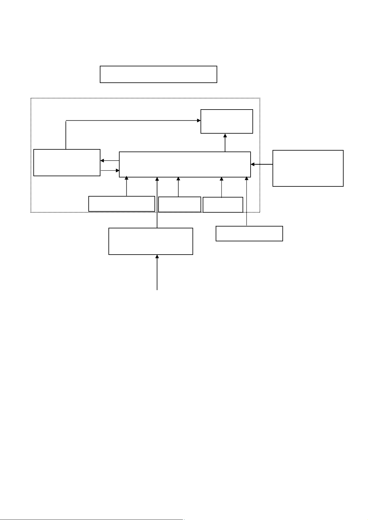
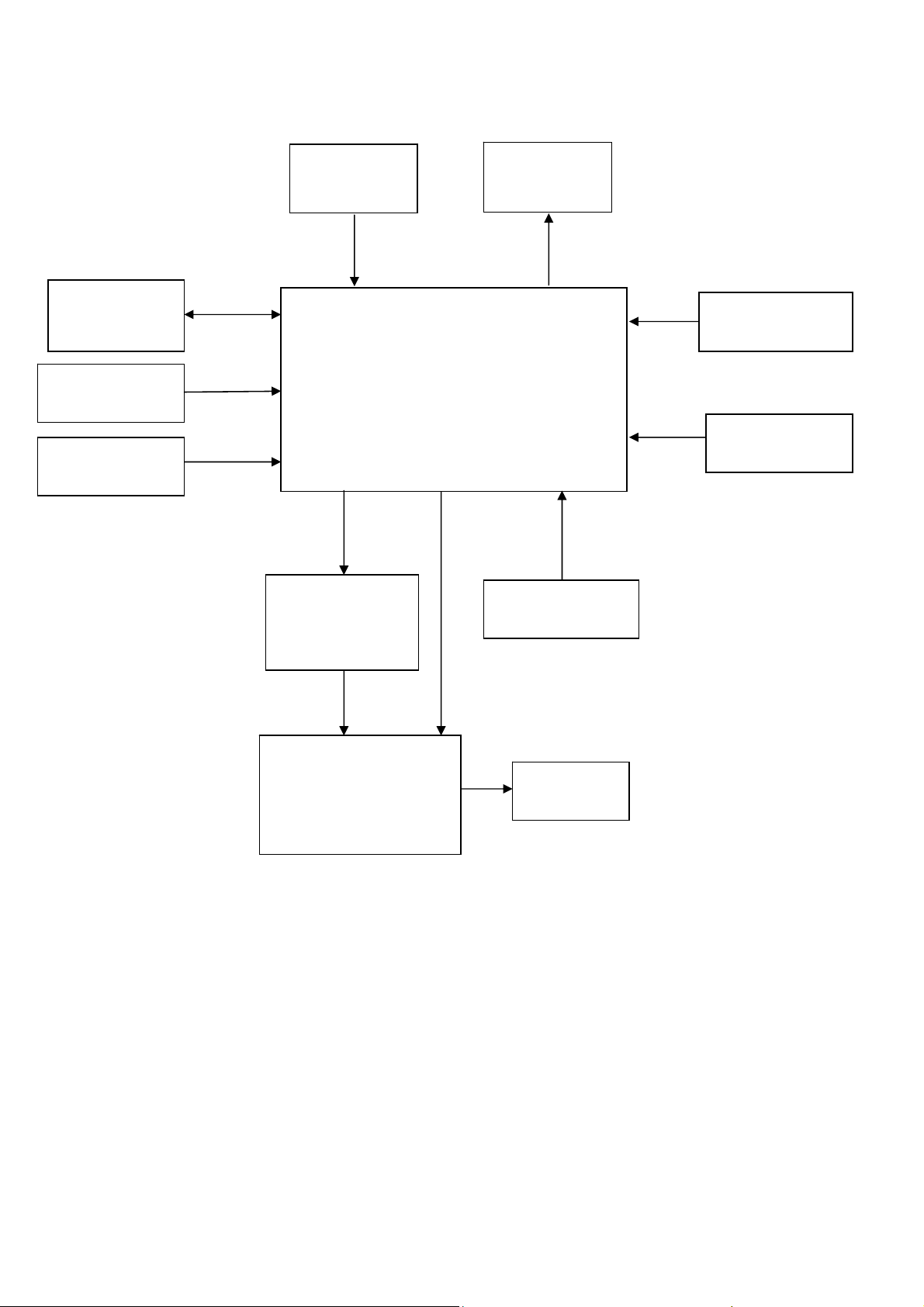
2. LCD Monitor Description
The LCD monitor will contain a main board, a converter board, a light sensor board, a LED board and a key board
which house the flat panel control logic, brightness control logic and DDC.
The converter board will provide DC to DC Inverter voltage to drive the backlight of panel.
Converter board
Light Sensor Board
Monitor Block Diagram
LED Drive.
Main Board
LED Board
Flat Panel and
LED backlight
Key Board
RS232 Connector
For white balance
adjustment in factory
mode
Adapter
100V-240V
AC-IN
HOST Computer
Video signal, DDC
5
Page 6
3. Operating Instructions
3.1 General Instructions
Press the power button to turn the monitor on or off. The other control knobs are located at front panel of the monitor.
By changing these settings, the picture quality can be adjusted to your personal preferences.
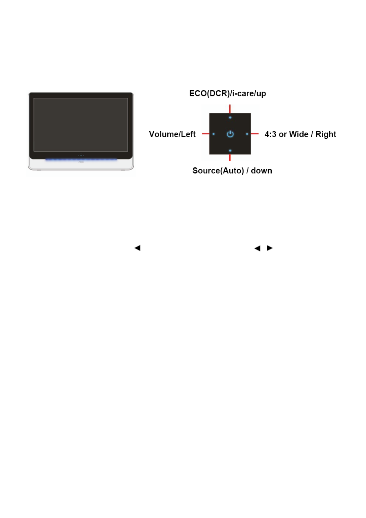
3.2 Control Buttons and Connections
Power Key
Press the Power button continuously about 2 second to turn off the monitor.
Eco Mode/DCR/i-care hot key
Press the Eco key continuously to select the Eco mode of brightness and DCR on when there is no OSD (Eco mode
hot key may not be available in all models).
i-care can detect the intensity of surrounding lights and automatically adjusts the monitor brightness according to
different light intensity
Volume adjustment hot key
When there is no OSD, press Volume (
for the models without speakers).
4:3 or wide image ratio hot key
When there is no OSD, press left hotkey continuously to change 4:3 or wide image ratio. (If the product screen size
is 4:3 or input signal resolution is wide format, the hot key is disable to adjust.)
Source hot key
When the OSD is closed, press Source (or Auto/Source) button will be Source hot key function (Only for the models
with dual or more inputs). Press Source button continuously to select the input source showed in the message bar,
press Menu/Enter button to change to the source selected.
Auto configure hot key
When the OSD is closed, press Auto/Source button continuously about 2 second to do auto configure (Only for the
models with dual or more inputs).
) to active volume adjustment bar, press or to adjust volume. (Only
6
Page 7
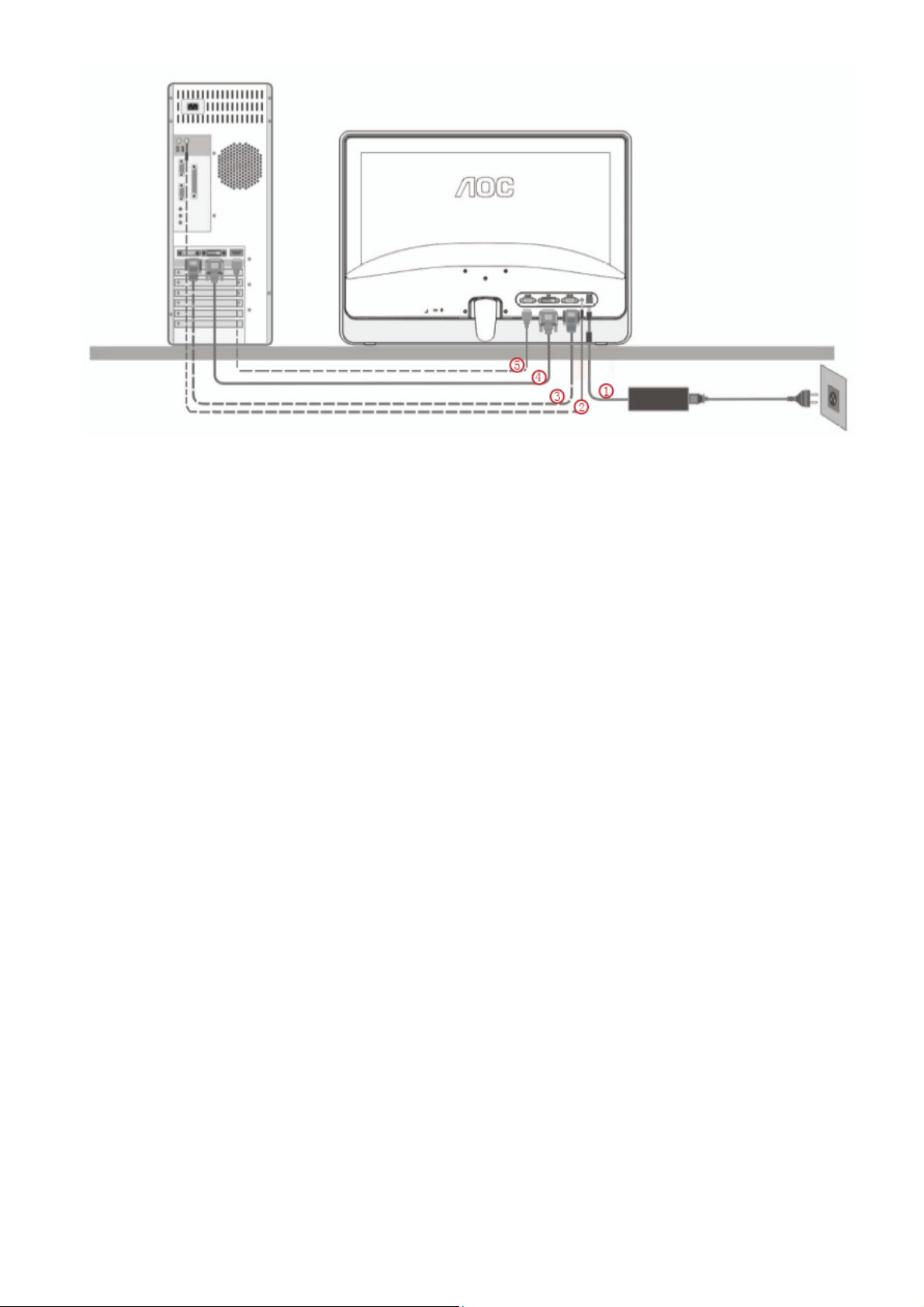
1. Power
2. Audio
3. Analog (DB-15 VGA cable)
DVI
4.
5. HDMI
To protect equipment, always turn off the PC and LCD monitor before connecting.
1 Connect the power cable to the AC port on the back of the monitor.
2 Connect one end of the 15-pin D-Sub cable to the back of the monitor and connect the other end to the computer's
D-Sub port.
3 (Optional – Requires a video card with DVI port) - Connect one end of the DVI cable to the back of the monitor and
connect the other end to the computer’s DVI port.
4 (Optional-Requires a video card with HDMI port) - Connect one end of the HDMI cable to the back of the monitor
and connect the other end to the computer's HDMI port.
5 Turn on your monitor and computer.
If your monitor displays an image, installation is complete. If it does not display an image, please refer
Troubleshooting.
7
Page 8

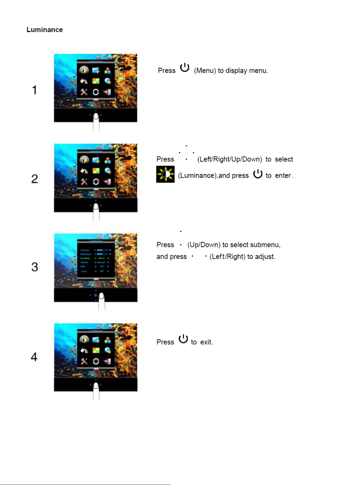
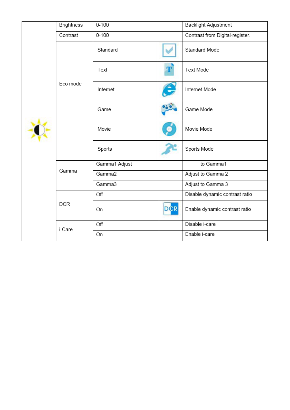
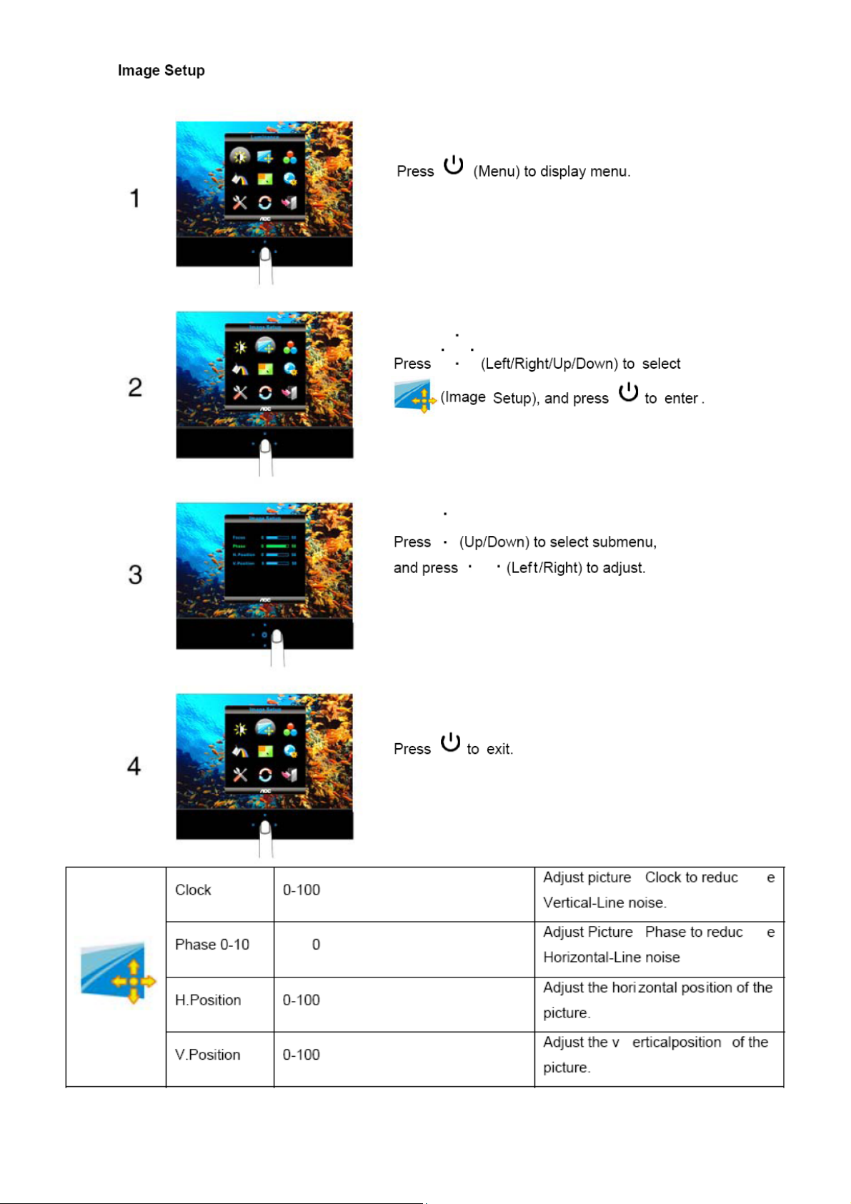
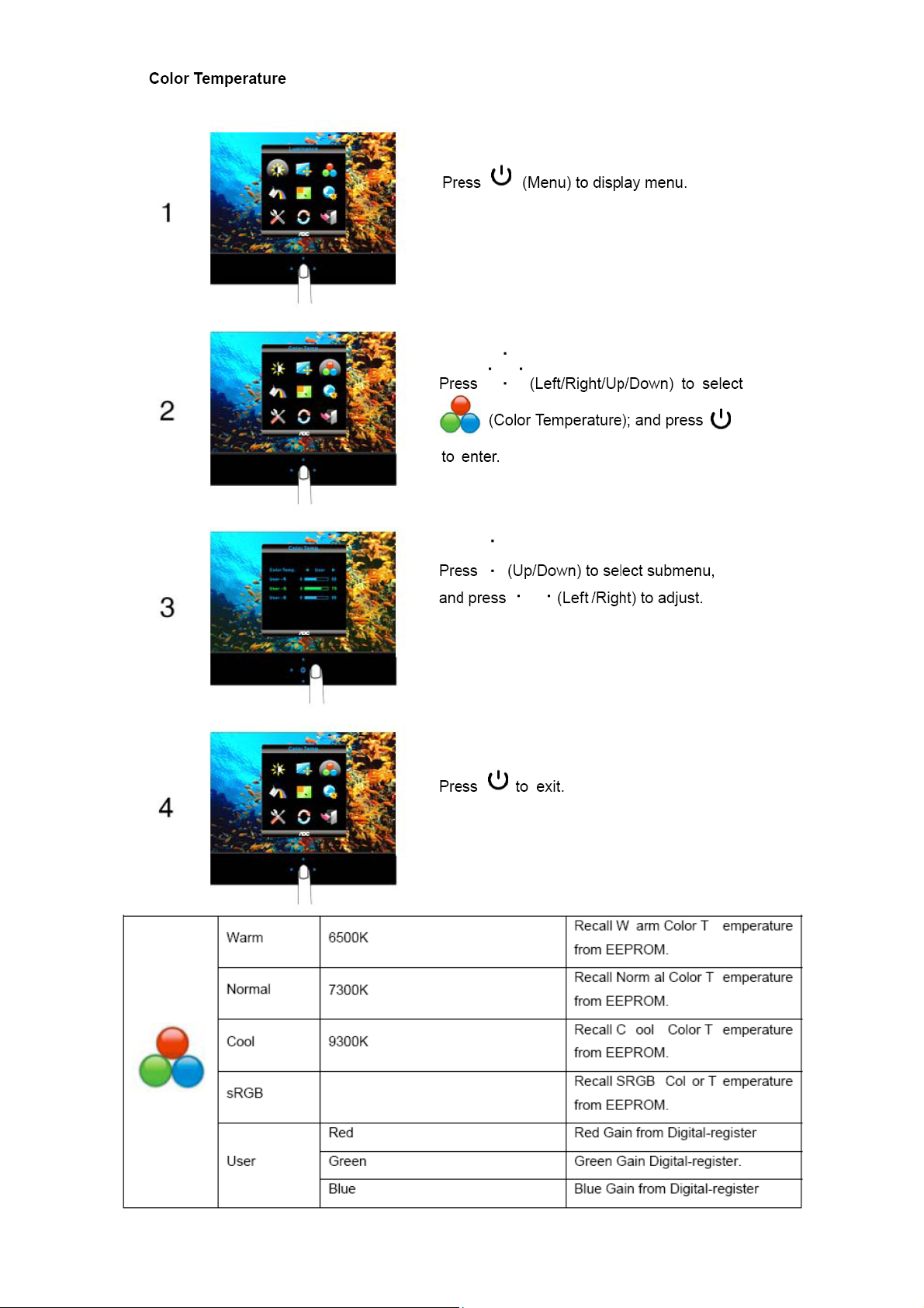
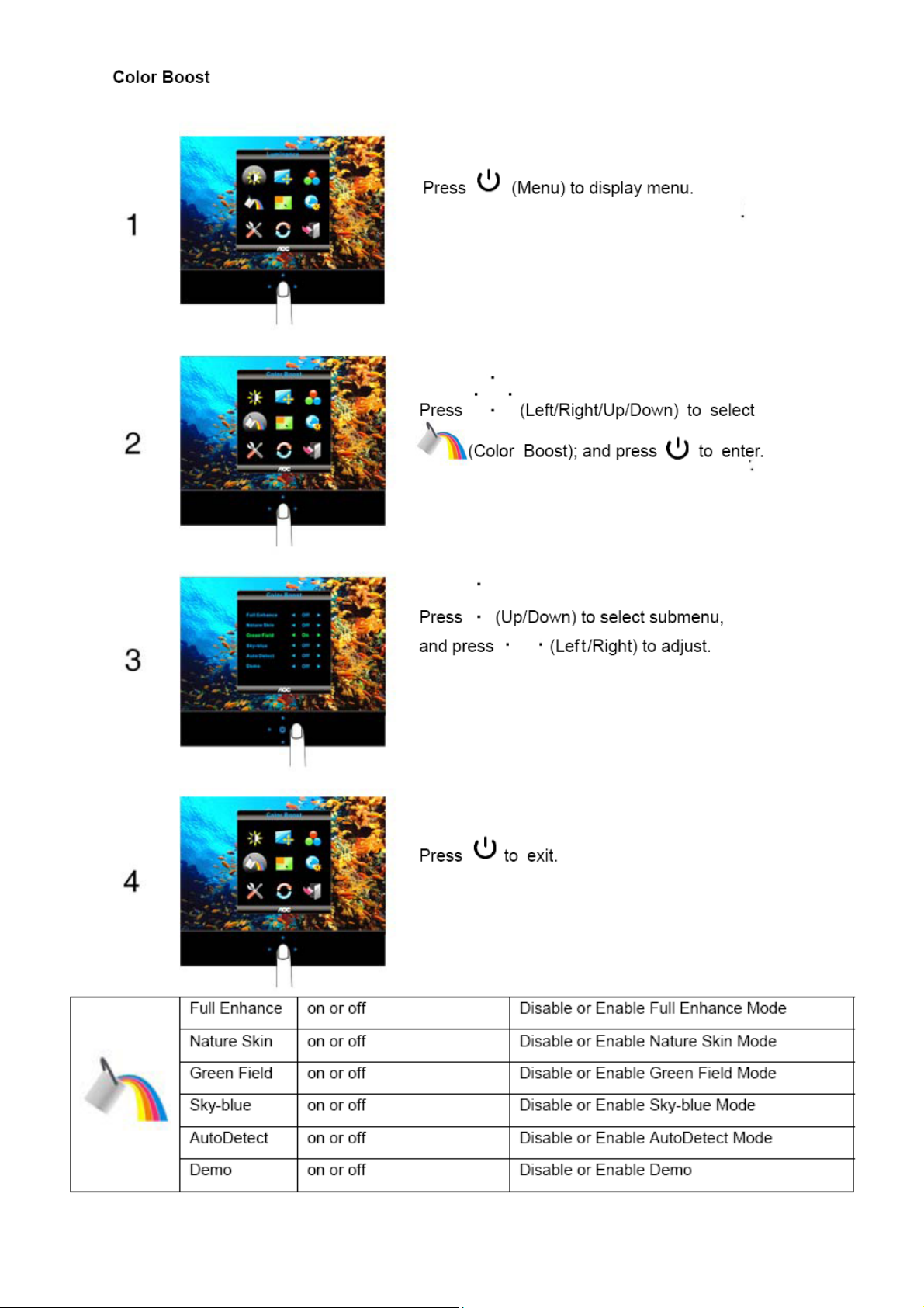
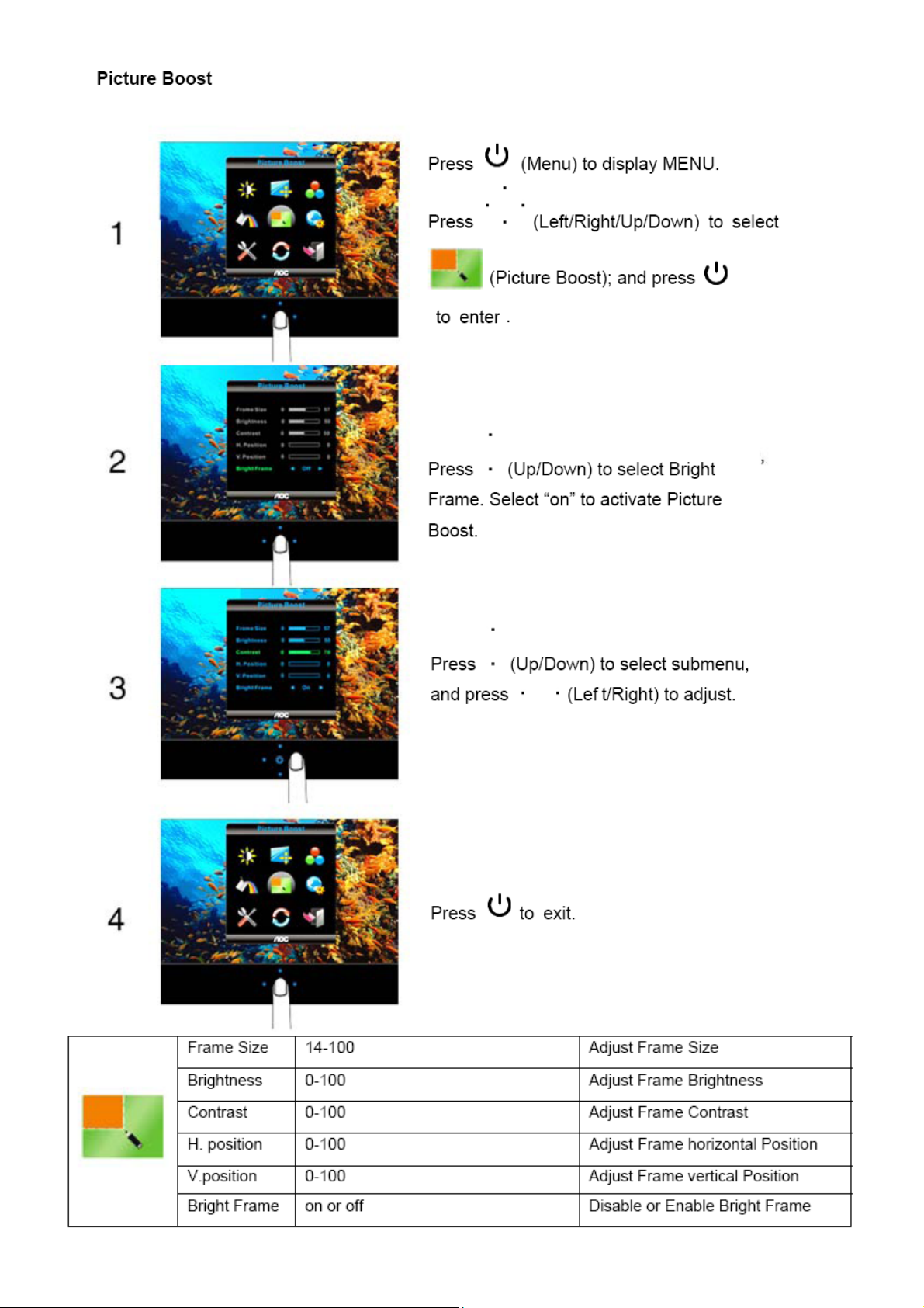
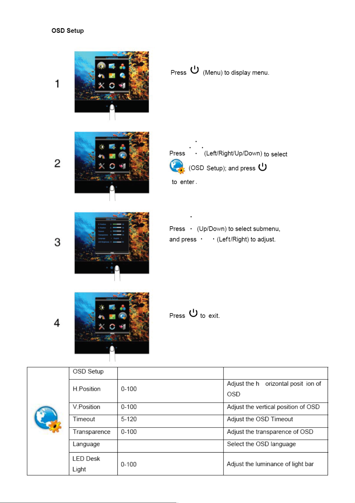
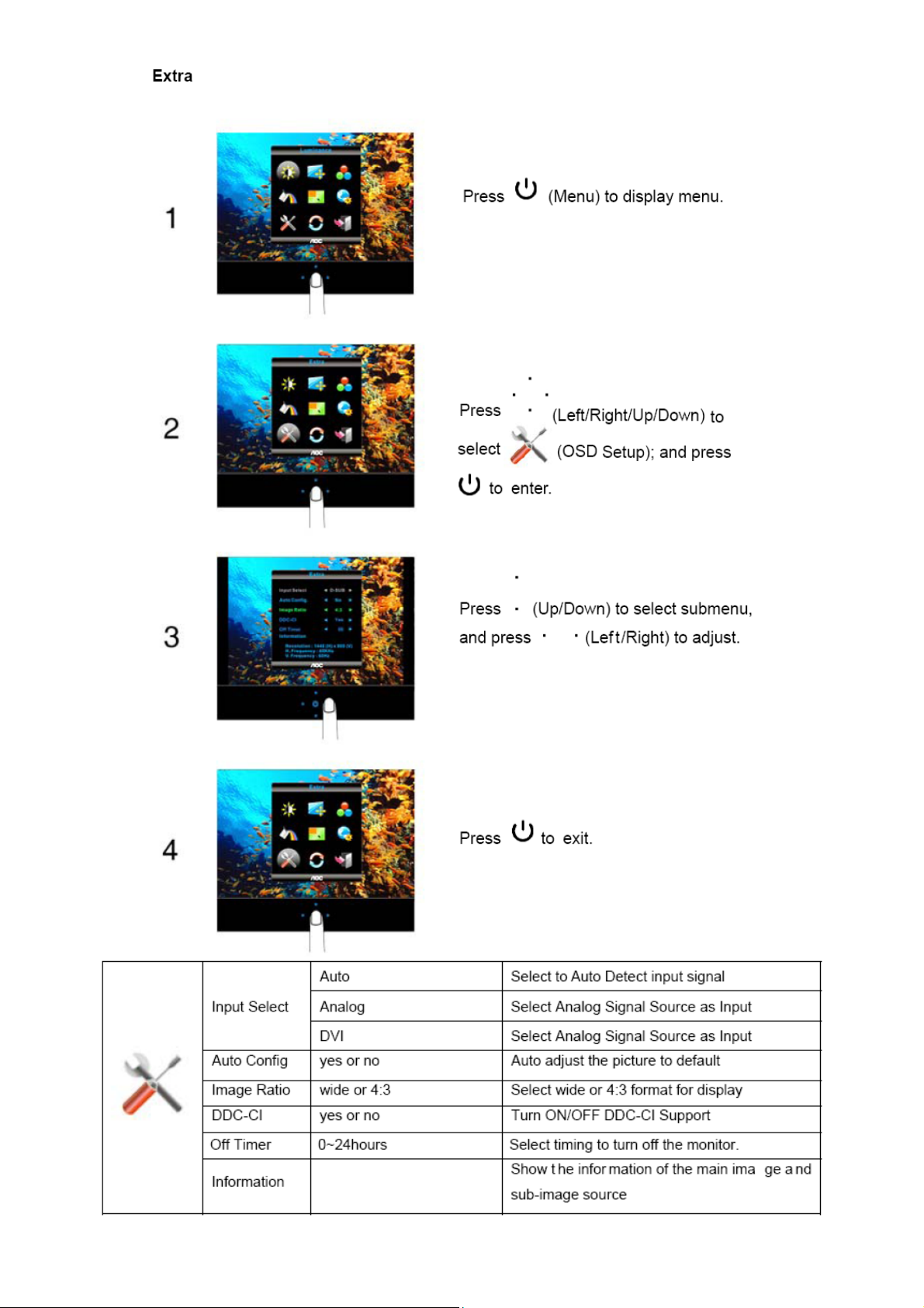
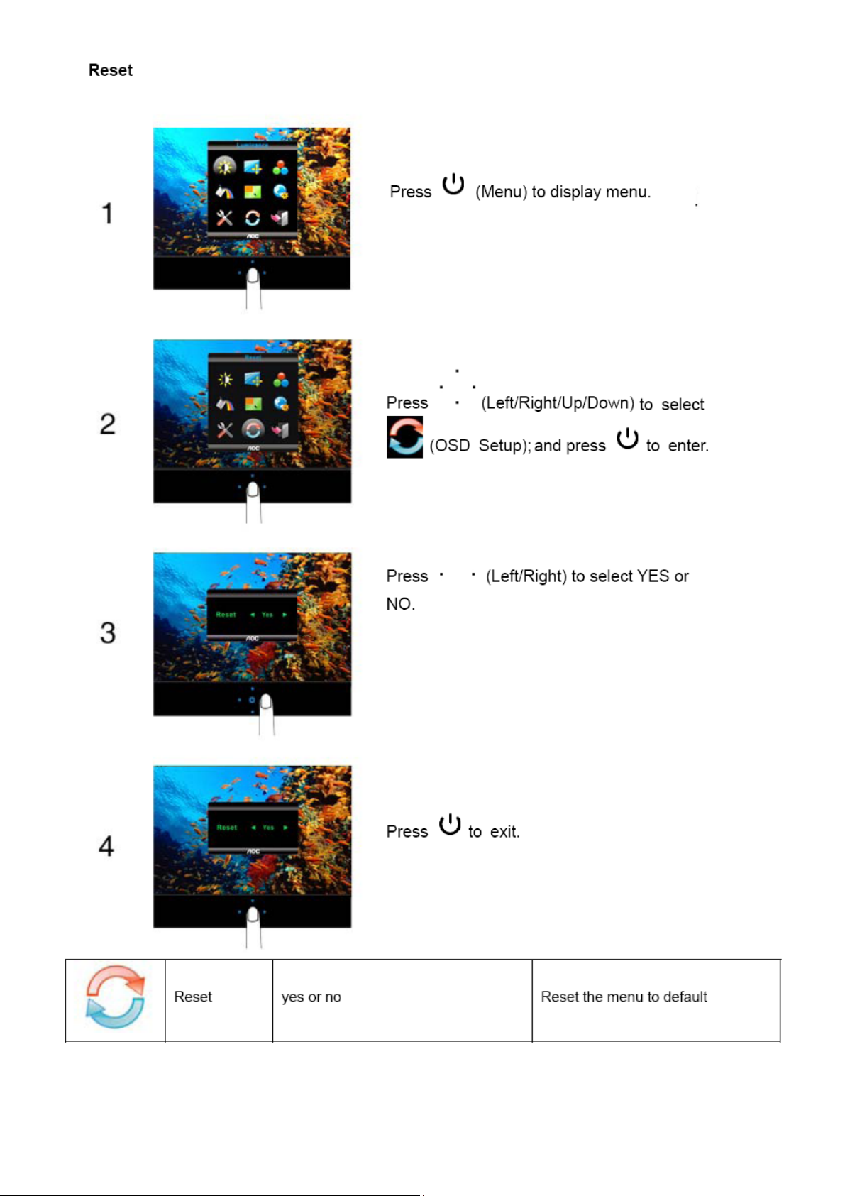
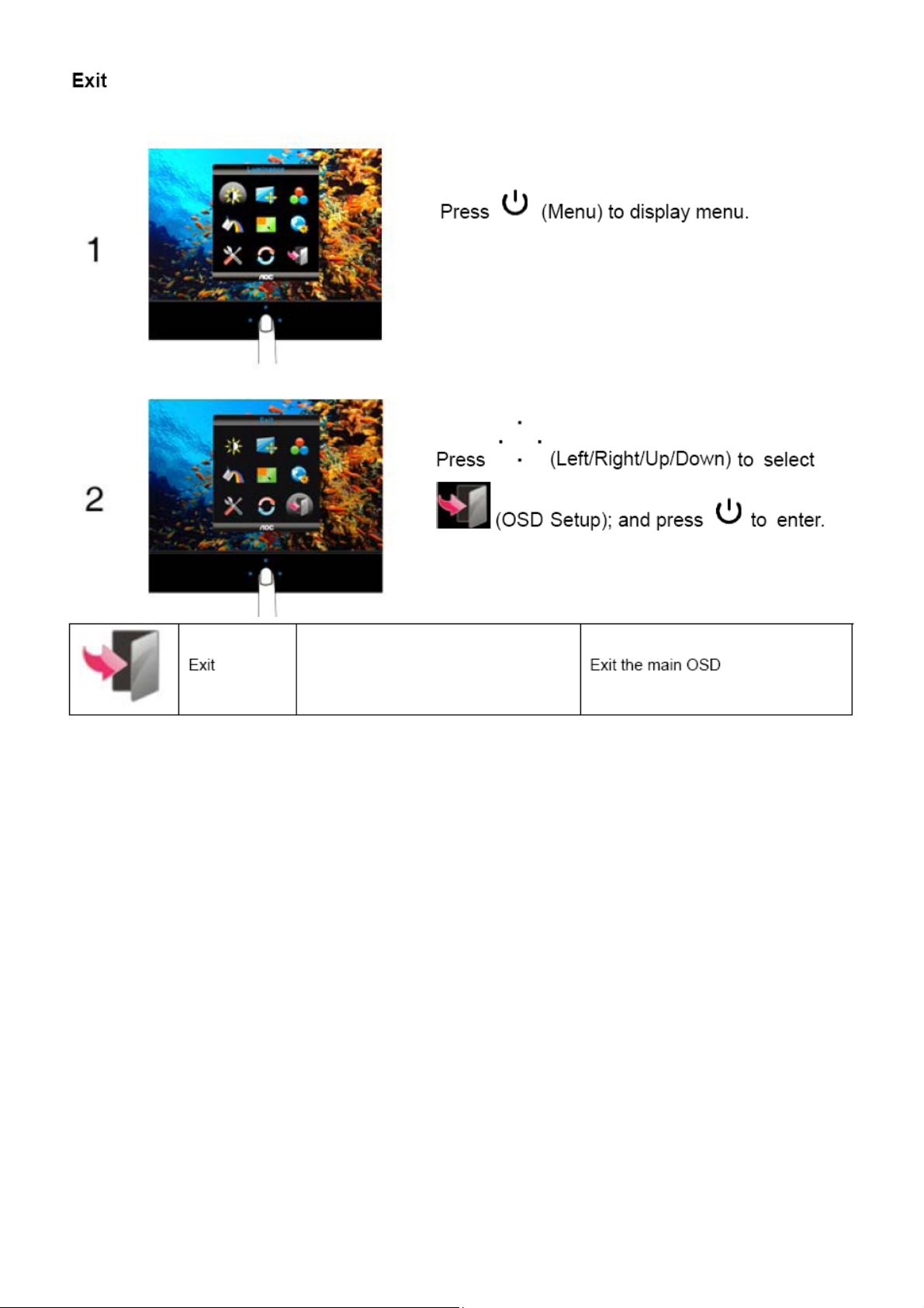
3.3 OSD Menu
1) Press Menu (Power) button to activate the OSD window. Press left, right, up, down button to navigate through
the functions. Once the desired function is highlighted, press Menu (Power) button to activate submenu.
2) In sub-menu, Press up, down button to navigate through the functions. Once the desired function is highlighted,
press left, right button to change the setting. Press Menu (Power) button to return to superior menu.
3) If you want to adjust any other function, repeat steps 1-2.
4) To exit OSD windows, select “exit” icon on main OSD, then press Menu (Power) button.
5) OSD Lock Function: To lock the OSD, press and hold the Left button while the monitor is off and then press
power button to turn the monitor on. To un-lock the OSD, press and hold the Left button while the monitor is off and
then press power button to turn the monitor on.
Notes:
1)If the product has only one signal input, the item of "Input Select" is disable to adjust.
2)If the product screen size is 4:3 or input signal resolution is wide format, the item of "Image Ratio" is disable to
adjust.
3)One of DCR, Color Boost, and Picture Boost functions is active, the other two function is turned off accordingly.
8
Page 9
9
Page 10
10 11 12 13 14 15 16 17 18
Page 11
Page 12
Page 13
Page 14
Page 15
Page 16
Page 17
Page 18
Page 19
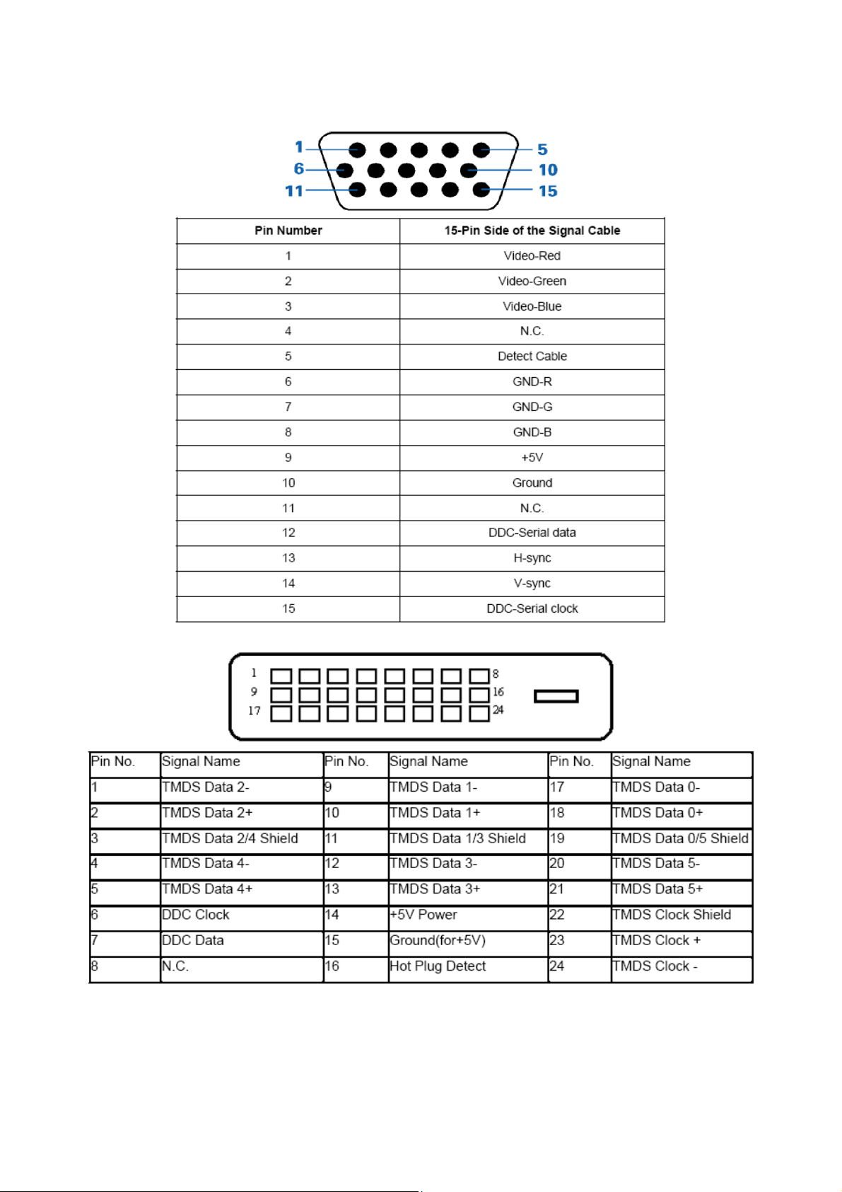
4. Input/Output Specification
4.1 Input Signal Connector
Analog connectors
DVI connectors
19
Page 20
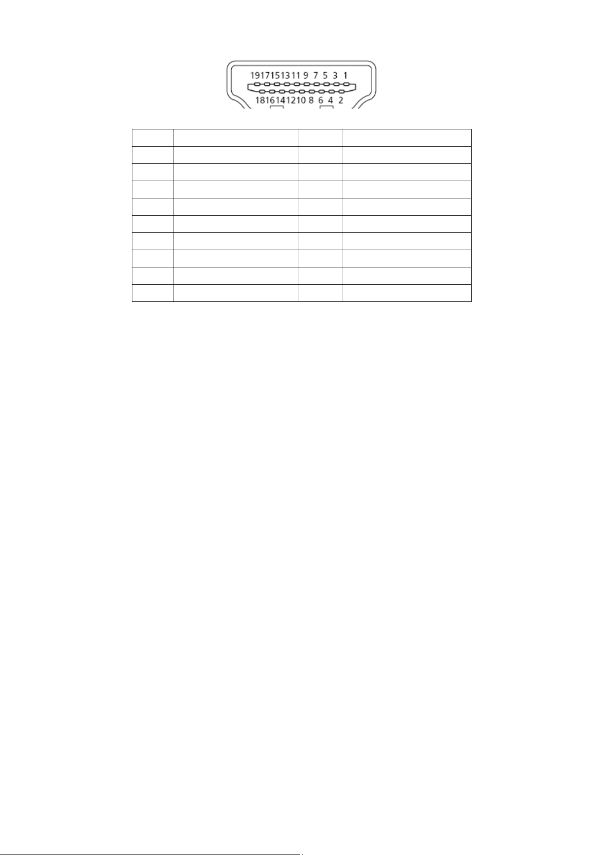
HDMI connectors
1 HDMI data 2+ 11 HDMI Clock Shield
2 HDMI data 2 Shield 12 HDMI Clock3 HDMI data 2- 13 CE remote
4 HDMI data 1+ 14 N/A
5 HDMI data 1 Shield 15 DDC Clock
6 HDMI data 1- 16 DDC Data
7 HDMI data 0+ 17 GND
8 HDMI data 0 Shield 18 +5V Power
9 HDMI data 0- 19 HP DET
10 HDMI Clock+
20
Page 21
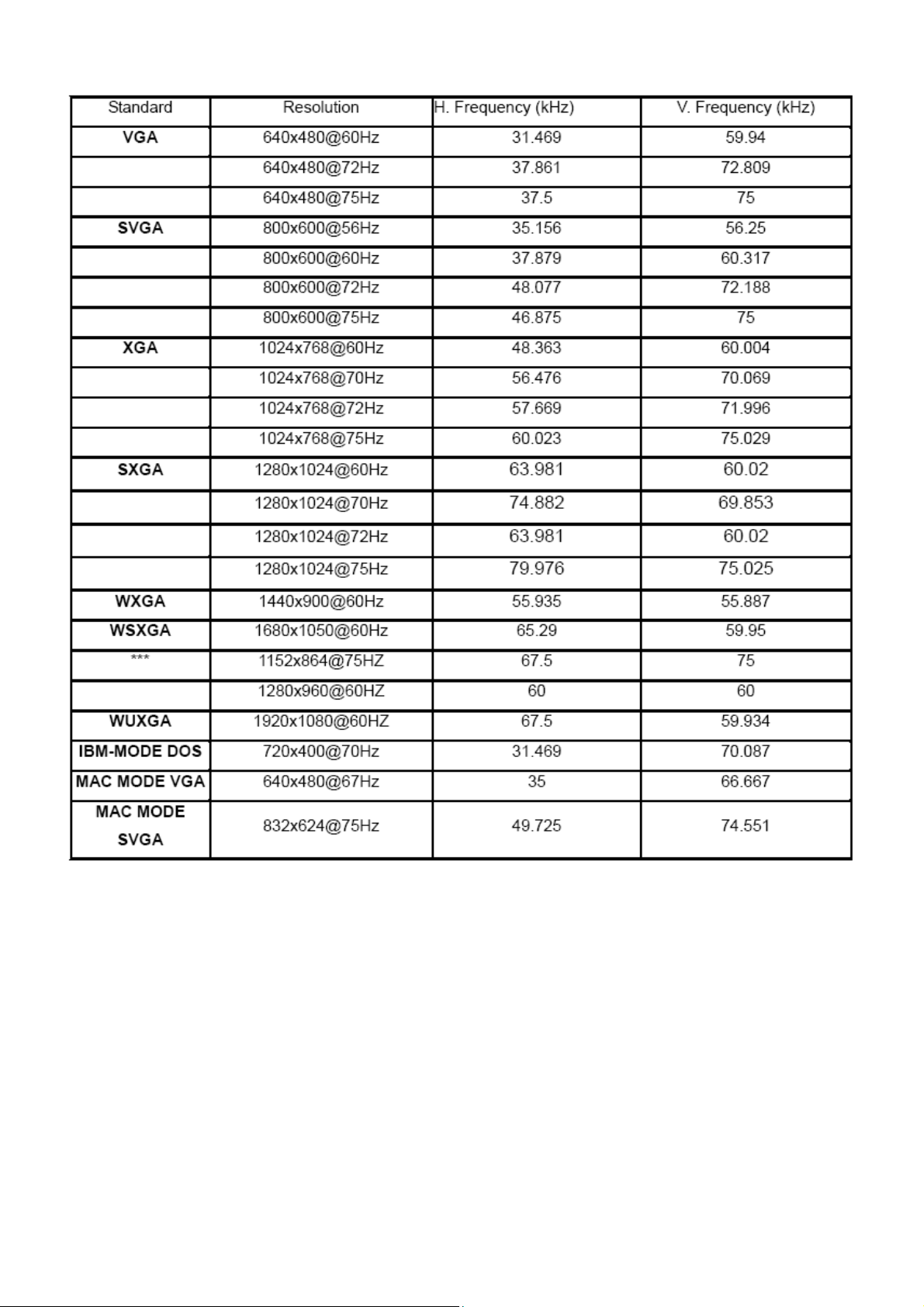
4.2 Factory Preset Display Modes
21
Page 22
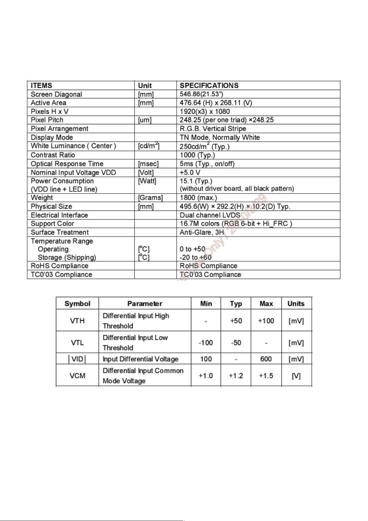
4.3 Panel Specification
4.3.1 General Features
This specification applies to the 21.5 inch-wide Color a-Si TFT-LCD Module M215HW01.The display supports the
Full HD - 1920(H) x 1080(V) screen format and 16.7M colors (RGB 6-bits + Hi-FRC data). All input signals are
2-channel LVDS interface and this module doesn’t contain a driver board for backlight.
4.3.2 Display Characteristics
4.3.3 Electrical Characteristics
22
Page 23
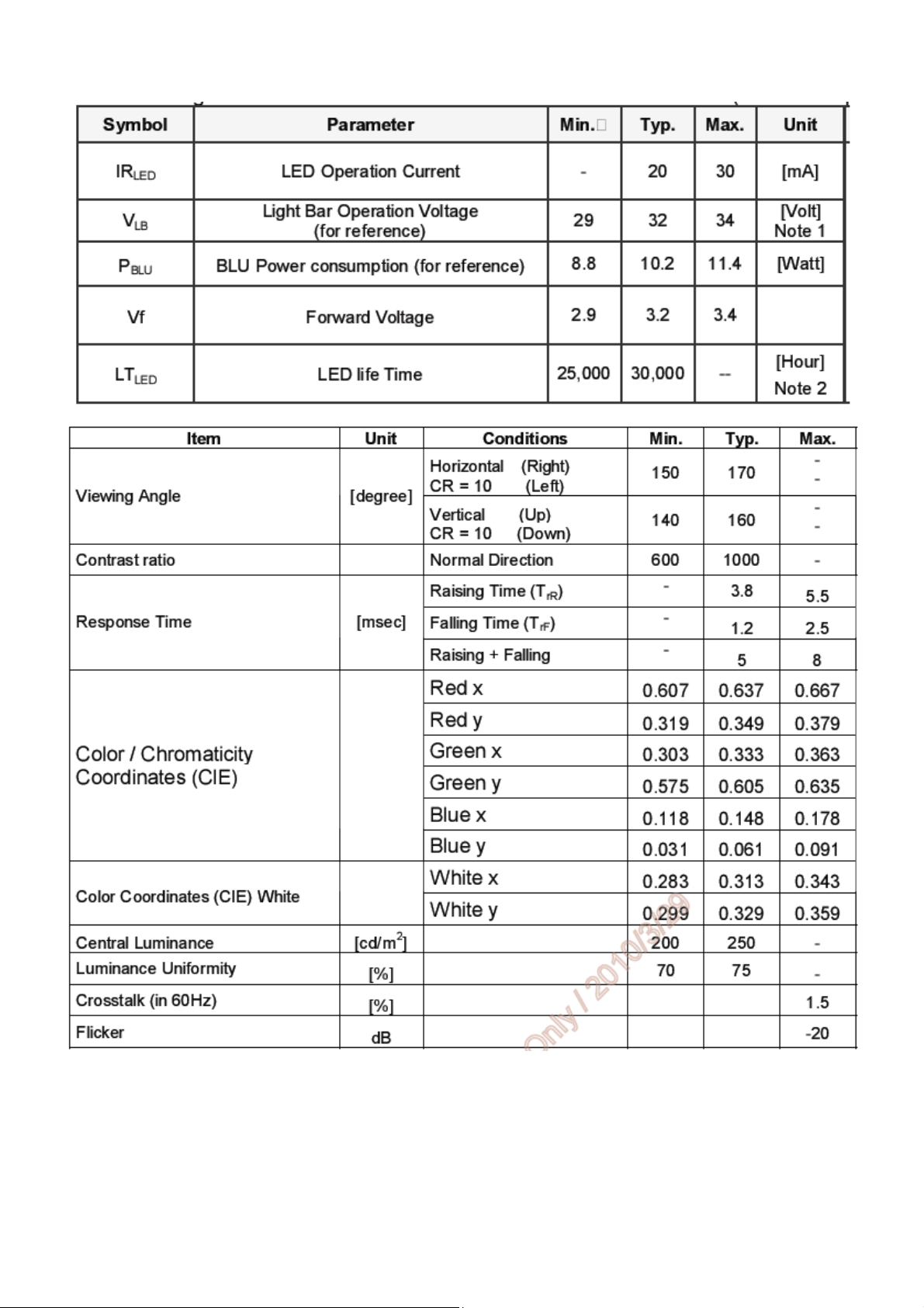
Backlight Unit
4.3.4 Optical Characteristics
23
Page 24
(
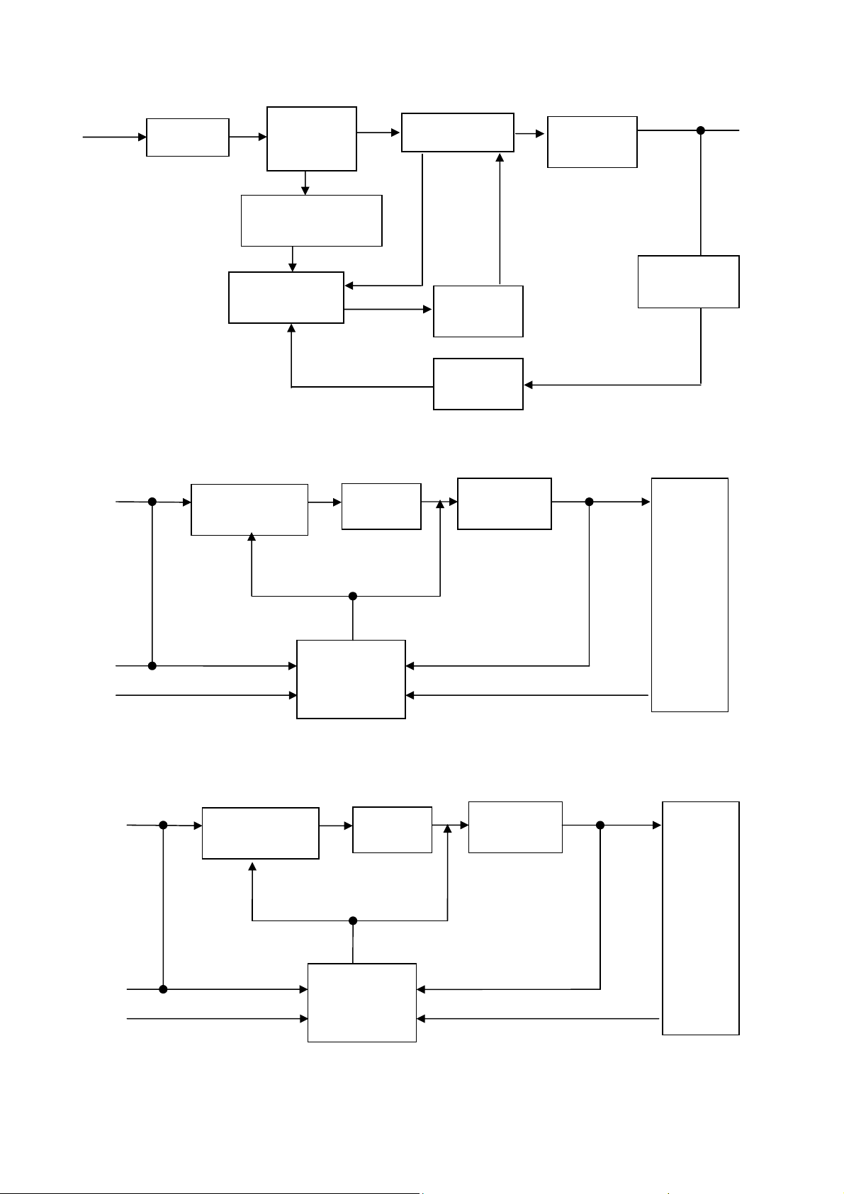
5. Block Diagram
5.1 Main Board
FLASH ROM
A25L020AO-F/Q
U402)
D-Sub Connector
(CN101)
Phone Jack
(CN601)
14.31818MHZ
(X401)
Scalar IC TSUMU88MWDT3-LF-1
(Include ADC, OSD, MCU)
Step-Down Converter
MP1584EN
(U602)
(U401)
Panel Interface
(CN301)
HDMI Connector
(CN501)
Key Control Interface
(CN401)
DVI Connector
(CN102)
Class-D Audio Amplifier
PAM8602MNHR
(U601)
Speaker
(CN602)
24
Page 25
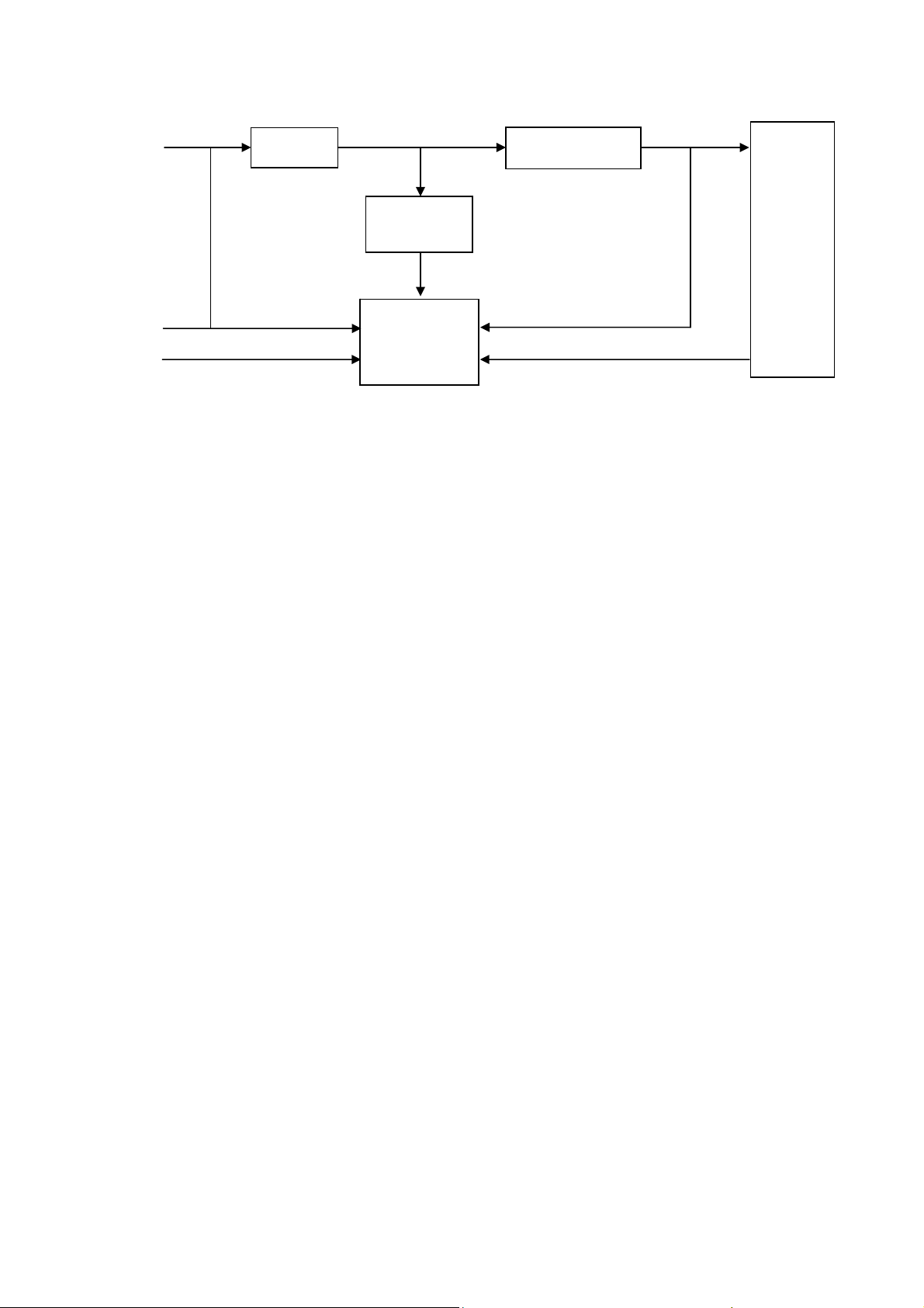
5.2 Power Board
AC input
EMI filter
Converter
12V
PWM
ON/OFF
12V
PWM
ON/OFF
Bridge
Rectifier
and Filter
Start Resistor
(R934, R906)
PWM Control
(IC901)
MOSFET
(Q801)
MOSFET
(Q802)
L801
PWM Control
OZ9955ALN
(U801)
L802
PWM Control
OZ9955ALN
(U802)
Transformer
Power Switch
(Q901)
Photo coupler
(IC902)
D801
D802
Rectifier
diodes
12V
Feedback
Circuit
LED
(CN802)
LED
(CN803)
25
Page 26
715G4128P02000004F
Converter
14.5V
DIM
ON/OFF
L801
MOSFET
(Q806)
PWM Control
MP3389EF
(U801)
D801
LED
(CN804)
26
Page 27
6. Schematic
6.1 Main Board
715G3603M02000004L
R101
DDC1_SCL5
DDC1_SDA5
DDC1_SCL
DDC1_SDA
CN102
JACK
VSYNC
SYNC GND
DDC SCL
DDC SDA
HPD
1/3shie ld
2/4shie ld
0/5shie ld
clk shield
DAT0+
DAT0-
DAT1+
DAT1-
DAT2+
DAT2-
DAT3+
DAT3-
DAT4+
DAT4-
DAT5+
DAT5-
clk+
GND
GND
26
25
100OHM1/16W
100OHM1/16W
+5V
clk-
8
15
6
7
14
16
11
3
19
22
18
17
10
9
2
1
13
12
5
4
21
20
23
24
R113
DVI_HPD
R102 0R05 1/10W
H_Sync
V_Sync
CN101
DB15
DSUB_SCL
DSUB_SDA
FB104
300 OHM
U107
AZC199-04S
1
I/O1
I/O4
2
GND
VDD
3 4
I/O2 I/O3
15
14
13
12
11
6
5
R106
2.2K1/16W
17 16
ESD_VCC1
10
5
9
4
8
3
7
2
6
1
DVI_5V
R120 10K1/16W
C115
100N 16V
U106
AZC199-04S
1
2
3 4
R107
2.2K1/ 16W
VGA_PLUG
VGA_BVGA_B+
VGA_GVGA_G+
VGA_RVGA_R+
I/O1
I/O4
GND
VDD
I/O2 I/O3
C103
22P 50V
DSUB_5V
ZD101
RLZ5.6B
R118 100OHM1/16W
R119 100OHM1/16W
ESD_VCC1
6
5
R103 1K1/16W
R104 1K1/16W
C104
22P 50V
DSUB_SDA
H_Sync
VGA_DET 5
C124
100N 16V
VGA_B+
VGA_G+
U105
AZC199 -04S
1
I/O1
I/O4
2
GND
VDD
3 4
I/O2 I/O3
1
2
3 4
1
2
3 4
DDC2_SCL
DDC2_SDA
R126 10OHM1/16W
R127 10OHM1/16W
R128 10OHM1/16W
R129 10OHM1/16W
R130 10OHM1/16W
R131 10OHM1/16W
R132 10OHM1/16W
R134 10OHM1/16W
ESD_VCC1
6
5
DSUB_H 5
DSUB_V 5
U104
AZC199-04S
I/O1
I/O4
GND
VDD
I/O2 I/O3
U103
AZC199-04S
I/O1
I/O4
GND
VDD
I/O2 I/O3
6
V_Sync
5
DSUB_SCL
VGA_R+
6
5
VGA_PLUG
DDC2_SCL 5
DDC2_SDA 5
RX0P
RX0N
RX1P
RX1N
RX2P
RX2N
RXCP
RXCN
ESD_VCC
ESD_VCC
RX0P 5
RX0N 5
RX1P 5
RX1N 5
RX2P 5
RX2N 5
RXCP 5
RXCN 5
VGA_B+
VGA_B-
VGA_G+
VGA_G-
VGA_R+
VGA_R-
BEAD
R108
75OHM1/16W
FB103
1 2 R111
BEAD
R112
75OHM1/16W
FB101
1 2
BEAD
R116
75OHM1/16W
R124
4.7K1/16W
DDC1_SCL
DDC1_SDA
DDC_WP5,6
DVI_5V
1
CMVCC1
R137
4.7K1/16W
DDC2_SCL
DDC2_SDA
2
ESD_VCC1
CMVCC13,4,5, 6,8
DDC_WP5,6
FB102
1 2
R125
4.7K1/16W
D102
BAV70
R138
4.7K1/16W
ESD_VCC
3
R105
10OHM1/16W
C105
5PF 50V
R109
47 OHM 1/16W
R110
470OHM1/16W
10OHM1/16W
C109
5PF 50V
R114
47 OHM 1/16W
R115
10OHM1/16W
C113
5PF 50V
R117
47 OHM 1/16W
CMVCC1
R123
10K1/16W
FB105
300 OHM
R136
10K1/16W
2
3
C102
47N 16V
C106
47N 16V
C107
1N 50V
C108
47N 16V
C110
47N 16V
C111
47N 16V
C114
47N 16V
DSUB_5V
1
D101
BAV70
U101
8
A0
VCC
7
A1
WP
6
A2
SCL
VSSSDA
AT24C02BN-SH-T
C120
100N 16V
U102
8
A0
VCC
7
A1
WP
6
A2
SCL
VSSSDA
AT24C02BN-SH-T
DSUB_B+ 5
DSUB_B- 5
DSUB_SOG 5
DSUB_G+ 5
DSUB_G- 5
DSUB_R+ 5
DSUB_R- 5
C116
220nF 16V
1
2
3
45
C117
220nF 16V
1
2
3
45
T P V ( Top Victory Electronics Co . , Ltd. )
Date
G3603-M1C-X-X-1-100420
2.0.IN PUT
絬 隔 瓜 絪 腹
Key Component
OEM MO DE L Size
TPV MOD EL
PCB NAME
Sheet
715G3603-M0J
of
38Tuesday, April 20, 2010
Rev
称爹
<
27
G
称爹
B
>
Page 28
CON301
3132
30
28
26
24
22
20
18
16
14
12
10
8
6
4
2
RXO0+
RXO1+
RXO2+
RXOC+
RXO3+
RXE0+
RXE1+
RXEC+
RXE3+
LVB0P
LVB1P
LVBCKP
LVB3P
LVA0P
LVA1P
LVA2P
LVACKP
LVA3P
PANEL_VCC
PA[0.. 9]5
PA[0..9]
PA0
PA1
PA2
PA3
PA4
PA5
PA6
PA7
PA8
PA9
LVA3P
LVACKP
LVACKM
LVA2P
LVA2M
LVA1P
LVA1M
LVA0P
LVA0M
PB[0.. 9]5
PB[0.. 9]
PB0
PB1
PB2
PB3
PB4
PB5
PB6
PB7
PB8
PB9
LVB3P
LVB3M
LVBCKM
LVB2P
LVB2M
LVB1P
LVB1M
LVB0P
LVB0M
LVB0M
LVB1M
LVB2MLVBCKP LVB2PLVA3M
LVBCKM
LVB3M
LVA0M
LVA1M
LVA2M R XE2+
LVACKM
LVA3M
RXO0RXO1RXO2RXOCRXO3RXE0RXE1RXE2RXECRXE3-
29
27
25
23
21
19
17
15
13
11
9
7
5
3
1
R301
PANEL_VCC
FB301
1 2
120 OHM
CMVCC1
CMVCC12,4,5, 6,8
R305
10K1/16W
R304
PPWR_ON #5
22K1/16W
R303
4.7K1/1 6W
C304
100N 16V
Q302
LMBT3904LT1G
R306
100K1/16W
3
1
G
R307
NC
D
2
S
C303
220nF 16V
Q301
AO3401
5
4
C305
1uF 16V
C302
22UF 16V
D
G
876
U301
DDD
NC/AO4411
SSS
123
R308
10K1/16W
CMVCC1
220 OHM 1/4W
R302
220 OHM 1/4W
C301
100N 16V
AO3401L
T P V ( Top Victory Electronics Co . , Ltd. )
絬 隔 瓜 絪 腹
Key Component
G3603-M1C-X-X-1-100420
3.0.OU TPUT
Date
OEM MO DE L Size
TPV MODEL
PCB NAME
Sheet
715G3603-M0J
48Tuesday, April 20, 2010
of
Rev
称爹
B
G
<
称爹
>
28
Page 29
U702
3 2
CMVCC1
CN702
1112
1
2
3
4
5
6
7
8
9
10
CONN
BKLT-VBRI
BKLT-EN
+12V
R707
NC / 0R 05 1/10W
R708
NC/0R 05 1/10W 5%
CMVCC1
12
D707
SM340A
12
D708
SM340A
VIN VOUT
GND
1
U701
NC/G1117- 33T43UF
ADJ(GND )
VOUT(TAB)
VIN
123
VCC3.3
BKLT-EN
BKLT-VBRI
C713
100nF 25V
CMVCC1
C702
100N 16V
R711 100K1/16W
100N 16V
R702
10K1/16W
Q701
LMBT3904LT1G
22K1/16W
C712
CMVCC1
R704
CMVCC1
R705
10K1/16W
R706 100OHM1/16W
R727
10uF 25V
33K 1/16W
R703
10K1/16W
C722
on_BACKLIGHT 5
C725100N 16V
9
8
7
6
R710
300K
adj_BACKLIGHT 5
FB702
1 2
30R/700mA
U705
Therm al Pad
SW
BST
EN
VIN
COMP
FREQ
FBGND
MP1584EN
1
2
3
45
150pF 50V
C724
R726
100K1/16W
SM340A
D701
1 2
SM340A
D702
1 2
VCC3.3
12
12
C720
1N 50V
D703
SM340A
D704
SM340A
C721
1N 50V
C705
100N 16V
C709
100N 16V
CMVCC1
VCC1.8
+
C716
470uF 10V
C707
22UF 16V
C704
22UF 16V
ZD702
NC/R LZ6.2B
1 2
C750
1UF 10V
CMVCC1 2,3,5,6,8
C708
100N 16V
U704
NC/G1117-1 8T63Uf
3 2
VI VO
GND
1
U703
3 2
VIN VOUT
C717
100N 16V
GND
1
C714
NC/1N 50V
C706
100N 16V
L701
22uH
R713
6K8 1/16W 1%
R714
1K3 +-1% 1/16W
1N 50V
CN701
JACK
C751
560PF 50V
T P V ( Top Victory Electronics Co . , Ltd. )
G3603-M1C-X-X-1-100420
絬 隔 瓜 絪 腹
Key Component
4.0.POWER
Date
OEM MODEL Size
TPV MODEL
715G3603-M0J
PCB NAME
of
58Wednesday , April 21, 2010
Sheet
C
G
Rev
称爹
>
<
称爹
+12V
+12V
FB701
1 2
BEAD
C723
+
C718
180uF 16V
C719
100nF 25V
3
2
1
29
Page 30
FB403
C401
220nF 16V
CMVCC1
R408
0R05OHM1/16W
LINE_OUTL8
LINE_OUTR8
VCC3.3
C419
10U 10V
C430
AUGND5
10N 50V
R412
10K1/16W
FB407
AUGND
300OHM
WP
R421
100K1/16W
LINE_INL8
LINE_INR8
C429
1uF 16V
C425 1N 50V
R427
AUCOM
AUVRM
AUVAG
10K1/16W
C444
10U 10V
U402
1
CS#
VCC
2
DO
HOLD#
3
WP#
CLK
4 5
VSS DI
MX25L2026MI -12G
C420 47pF 50V
C421 47pF 50V
C427 1uF 16V
C428 1uF 16V
R426
10K1/16W
C426 1N 50V
DSUB_R+2
DSUB_R-2
DSUB_G+2
DSUB_G-2
DSUB_SOG2
DSUB_B+2
DSUB_B-2
DSUB_H2
DSUB_V2
DDC1_SDA2
DDC1_SCL2
RX2P2
RX2N2
RX1P2
RX1N2
RX0P2
RX0N2
RXCP2
RXCN2
DDC2_SDA2
DDC2_SCL2
HD0-6
HD0+6
HD1-6
HD1+6
HD2-6
HD2+6
HCK-6
HCK+6
DDCD_SDA6
DDCD_SCL6
R401
AVDD
390R 1/16W 1%
100N 16V
8
7
6
R423 0R05OHM1/16W
X401
14.31818MHz
1 2
R428 100OHM1/16W
C422 100N 16V
AUCOM
AUVAG
AUVRM
R410 100OHM1/16W
R411 100OHM1/16W
AUGND
FB402
VCC3.3
1 2
120 OHM
C417
63
RIN0P
62
RIN0M
60
GIN0P
59
GIN0M
61
SOGIN0
58
BIN0P
57
BIN0M
66
HSYNC0
67
VSYNC0
69
DDCA_SDA/RS232_TX
70
DDCA_SCL/ RS232_RX
48
RXA2P
49
RXA2N
51
RXA1P
52
RXA1N
54
RXA0P
55
RXA0N
46
RXACKP
47
RXACKN
42
DDCDA_SDA
43
DDCDA_SCL
30
RXB2P
31
RXB2N
33
RXB1P
34
RXB1N
36
RXB0P
37
RXB0N
28
RXBCKP
29
RXBCKN
21
DDCDB_SDA
22
DDCDB_SCL
44
REXT
65
REFP
64
REFM
76
SDO
77
CSZ
78
SCK
79
SDI
8
RST
26
XIN
25
XOU T
3
BYPASS
68
MODE
89
LINEIN_L0
90
LINEIN_R 0
91
VCOM
93
VAG
94
VRM
96
LINEOUT_L
97
LINEOUT_R
99
SSPKL
100
SSPKR
AVDD_AU
C442
10U 10V
AUGND
AVDD_EAR
AVDD
VDDC
27
35
24
75
45
88
98
553106
VDDC
VDDC
VDDC
VDDC
VDDC
AVDD_33
AVDD_33
AVDD_33
AVDD_33
AVDD_EAR
TSUMU88MWDT3-LF-1
SPDIFO/C EC_BUS/GPIO_P42
GND
GND
GND
GND
GND
GND
GND
GND
6
12
323850
87
95
101
C408
100N 16V
ADC1.8
AVDD_AU
VDDP
13
56
7
92
105
VDDP
VDDP
VDDP
AVDD_18
AVDD_AUSDM
GPIO_P04/PWM3
GPIO_P23/PWM1
GPIO_P25/PWM3
GPIO_P00/SAR0
GPIO_P01/SAR1
GPIO_P02/SAR2
GPIO_P03/SAR3
GPIO_P13/PWM2
GPIO_P26/PWM0
GPIO_P27/PWM1
GPIO_P14/PWM0
AUMUTE/GPIO_P43
GPIO_P24/PWM2/SPDIF O
I2C_MCL/GPIO_P10
I2C_MDA/GPIO_P11
GND
118
117
74
VCTRL
VDDP
VDDP
LVA3M
LVACKP
LVACKM
LVA2M
LVA1M
LVA0M
LVB3M
LVBCKP
LVBCKM
LVB2M
LVB1M
LVB0M
GPIO_P05
GPIO_P17
GPIO_P06
GPIO_P07
GPIO_P15
GPIO_P16
AUOUTLR
AUSCK
GPIO_11
GPIO_12
GPIO_06
LVA3P
LVA2P
LVA1P
LVA0P
LVB3P
LVB2P
LVB1P
LVB0P
MCKO
AUSD
4
107
108
109
110
111
112
113
114
115
116
119
120
121
122
123
124
125
126
127
128
104
18
103
71
9
14
15
16
17
19
20
23
40
41
10
11
39
80
81
82
83
84
85
86
73
72
1
2
102
PA0
PA1
PA2
PA3
PA4
PA5
PA6
PA7
PA8
PA9
PB0
PB1
PB2
PB3
PB4
PB5
PB6
PB7
PB8
PB9
R422 100OHM1/16W
R434 100OHM1/16W
R415 100OHM1/16W
R416 100OHM1/16W
R417 100OHM1/16W
R425 NC/100OHM1/16W
R409 100OHM1/16W
R436 100OHM1/16W
R437 100OHM1/16W
R424 470OHM1/16W
PA[0..9]
PB[0..9]
KEY1
KEY2
LED_ORANGE
LED_GRN/BLUE
POWER_KEY#
WP
R438
10K1/16W
MSCL
MSDA
PA[0..9] 3
PB[0..9] 3
PPWR_ON# 3
on_BACKLI GHT 4
Volume 8
HDMI_HPD 6
adj_BACKLIGHT 4
CEC_CTRL 6
VCC3.3
R439
10K1/16W
MUTE 8
R406
22K1/16W
VCC1.8
VCC3.3 VDDP
VCC3.3
R435
10K1/16W
VCC3.3
R407
10K1/16W
1 2
120 OHM
1 2
VGA_DET 2
1
2
3
4
FB404
120 OHM
65
CN402
CONN
C416
100N 16V
ADC1.8
VCC3. 3
C414
10U 10V
AVDD_EAR
C418
10U 10V
R418
3.9K1/16W
DVI_HDMI_5V_DET 6
Q401
LMBT3904LT1G
FB401
VCC3.3
C415
100N 16V
C413
100N 16V
DDC_WP 2,6
絬 隔 瓜 絪 腹
Key Component
1 2
120 OHM
VCC3. 34
VCC1. 84
CMVCC12,3,4,6, 8
LMBT3906LT1G
R403
LED_G
0R05 1/10W
R405
LED_R
0R05 1/10W
CN401
89
1
2
3
4
5
6
7
CONN
T P V ( Top Victory Electronics Co . , Ltd. )
G3603-M1C-X-X-1-100420
5.0.SCALER
Date
KEY1
KEY2
POWER_KEY #
LED_G
LED_R
AVDD
C443
10U 10V
VCC3.3
1 2
VCC1.8
1 2
CMVCC1
Q402
FB408
1 2
120OHM
FB409
1 2
NC/120 OHM
C407
100N 16V
FB405
120 OHM
FB406
VDDC
120 OHM
NC/ 0R05 1/16W
R402
4.7K1/16W
23
1
LMBT3906LT1G
C432
C431
100N 16V
100N 16V
LED_R
OEM MODEL Size
TPV MOD EL
PCB NAME
Sheet
C436
100N 16V
C402
10U 10V
C440
10U 10V
R413
Q403
R431
CMVCC1
715G3603-M0J
CMVCC1
NC/3.9K1/16W
C433
NC/0.1uF 16V
68Wednesday , April 21, 2010
C403
100N 16V
C409
100N 16V
23
of
C437
100N 16V
VCC3.3
1
R432
ZD401
C404
100N 16V
C410
100N 16V
R414
0R05OHM1/16W
R404
4.7K1/16W
VCC3. 3
C434
NC/RLZ5.6B
C438
100N 16V
4.7K1/16W
4.7K1/16W
3.9K1/16W
NC/0.1uF 16V
C405
C406
100N 16V
C412
100N 16V
LED_ORAN GE
3.9K1/16W
C435
NC/0.1uF 16V
Rev
称爹
ZD403
C439
100N 16V
C441
100N 16V
NC/RLZ5.6B
C
G
称爹
>
<
100N 16V
C411
100N 16V
R419
LED_GRN/BLUE
R420
R433
ZD402
NC/RLZ5.6B
30
Page 31

U501
CN501
HDMI
D2 Shield
D1 Shield
D0 Shield
CK Shield
CE Remote
20
TH1
TH2
DDC DATA
TH3
TH4
TH5
Q504
LMBT3904LT1G
DDC CLK
HP DET
21
22
23
24
R521 1K1/16W
GND
D2+
D2-
D1+
D1-
D0+
D0-
CK+
CK-
+5V
AZ1045-04F
HDMI1_C KHDMI1_C K+
HDMI1_D 0HDMI1_D 0+
HDMI1_D2+
1
2
HDMI1_D2-
3
4
HDMI1_D1+
5
HDMI1_D1-
6
HDMI1_D0+
7
8
HDMI1_D0-
9
HDMI1_CK+
10
11
HDMI1_CK-
12
CEC
13
14
NC
15
16
17
18
19
R524
47K1/16W
HDMI_CLK
HDMI_DATA
HDMI_HOTPLUG
HDMI_+5V
R519
47K1/16W
C503
100N 16V
FB502
300 OHM
R516
1K1/16W
R510
0R05OH M1/16W
1
2
3 4
CMVCC1
R517
4.7K1/ 16W
U503
I/O1
I/O4
GND
VDD
I/O2 I/O3
AZC199-04S
6
5
HDMIESD
C501
100N 16V
NC/R526
NC/ 0R05OHM1/16W
CMVCC1
HDMI1_D 1HDMI1_D 1+
HDMI1_D 2HDMI1_D 2+
1
IN1
2
IN2
4
IN3
5 6
IN4 NC
8
U502
AZ1045-04F
1
IN1
2
IN2
4
IN3
5 6
IN4 NC
8
CEC_CTRL 5
R514 100 OHM1/16W
R515 100 OHM1/16W
DDCD_SDA5
DDCD_SCL5
DDC_WP2,5
GND
GND
10
HDMI1_CK-
NC
9
HDMI1_CK+
NC
7
HDMI1_D0-
NC
GND
3
GND
3
HDMI1_D0+
HDMI1_D1-
10
NC
HDMI1_D1+
9
NC
HDMI1_D2-
7
NC
HDMI1_D2+
R511
4.7K1/16W
R501 0R05OH M1/ 16W
R502 0R05OH M1/ 16W
R503 0R05OH M1/ 16W
R504 0R05OH M1/ 16W
R505 0R05OH M1/ 16W
R506 0R05OH M1/ 16W
R507 0R05OH M1/ 16W
R508 0R05OH M1/ 16W
HDMIESD
R512
4.7K1/16W
CMVCC1
R513
10K1/16W
2
1
3
HCKHCK+
HD0HD0+
HD1HD1+
HD2HD2+
HDMI_+5V
D501
BAT54C
U504
8
A0
VCC
7
A1
WP
6
A2
SCL
VSSSDA
AT24C02BN-SH-T
HCK- 5
HCK+ 5
HD0- 5
HD0+ 5
HD1- 5
HD1+ 5
HD2- 5
HD2+ 5
1
2
3
45
C502
220nF 16V
Q502
DVI_HDMI_5V_DET5
DVI_5V
FB501
300 OHM
R523
47K1/16W
R525
47K1/16W
R522
2K OHM
Q505
LMBT3904LT1G
ZD501
RLZ5.6B
LMBT3904LT1G
Q503
LMBT3904LT1G
R518 10 K1/16W
R520
10K1/16W
HDMI_HPD
HDMI_HPD 5
T P V ( Top Victory Electronics Co . , Ltd. )
絬 隔 瓜 絪 腹
Key Component
G3603-M1C-X-X-1-100420
7.0.HD MI INPU T
Date
OEM MODEL Size
TPV MODEL
PCB NAME
Sheet
715G3603-M0J
of
78Wednes day , April 21, 2010
Rev
称爹
B
G
称爹
>
<
31
Page 32

+12V
D601
LL4148
+12V
CN601
PHONEJAC K
4
5
3
2
1
R601
L
7.5K 1/16W
R602
R
7.5K 1/16W
LINE_IN L 5
LINE_IN R 5
+12V
R612
NC/100K1/ 16W
C602
100N 16V
NC/33K 1/ 16W
Del bead, Add GND area
R605
10K1/16W
R620
1
R606
1K1/16W
23
Q603
LMBT3906LT1G
C601
10uF 25V
C609
22UF 16V
C636100N 16V
9
8
7
6
R611
470K 1/16W 5%
R607
10K1/16W
1 2
U602
Therm al Pad
BST
VIN
FREQ
MP1584EN
MUTE5
FB605
30R/700mA
SW
EN
COMP
FBGND
MUTE
C606
100N 16V
1
2
3
45
C635
150pF 50V
R621
100K 1/16W 5%
+5V_AUDIO
R608
NC/10K1/ 16W
Q604
LMBT3904LT1G
SM340A
D602
1 2
C652
1nF 50V
22uH
L601
MUTE
R615
10K1/16W
R613
12K 1/16W 1%
R614
2.21K 1%
Volume5
C605
NC/100N 16V
+5V_AUDIO
C603
1N 50V
MUTE
LOW
R609
10K1/16W
C604
+
470uF 10V
R610
10K1/16W
+5V_AUDIO
ZD603
RLZ6.8B
1 2
LINE_OUTR5
POWER OFF
C653
100N 16V
VOL
C650
1UF 10V
MUTE
AUGND5
C626
1uF 16V
LINE_OUTL5
AUGND
C651
100N 16V
C612 1uF 16V
C607 220pF 50V
C611 1uF 16V
R603
10K1/16W
R604
10K1/16W
C608 220pF 50V
VOL
12
NC
NC
13
11
Volume
VREF
C617
1uF 16V
R617
0R05 1/10W
C613
1uF 16V
1uF 16V
10
9
VDC
NC
15
16
AUGND
AUGND
OUT-L+
OUT-LOUT-R+
OUT-R-
C615
1uF 16V
C614
NC
NC
17 8
C616
10U 10V
4
6
3
2
5
718
VDDGND
PVDD
PGND
-OUTL
/ MUTE
INR INL
PGND
PVDD
-OUTR
/ SHDN
22
23
201421
19
C618
1uF 16V
C619
10U 10V
CN602
4
3
2
1
CONN
FB601 120 OHM
1 2
FB602 120 OHM
1 2
1
PGND
+OUT L
U601
PAM8602MNHR
+OUT R
PGND
FB603 120 OHM
24
1 2
FB604 120 OHM
1 2
C620
1N 25V
C622
1N 25V
C624
220P 50V
C621
1N 25V
C625
220P 50V
C623
1N 25V
OUT-L+
OUT-L-
OUT-R-
OUT-R+
HI
POWER ON
T P V ( Top Victory Electronics Co . , Ltd. )
G3603-M1C-X-X-1-100420
絬 隔 瓜 絪 腹
Key Component
6.0.AUD IO
Date
OEM MOD EL Size
TPV MODEL
PCB NAME
Sheet
715G3603-M0J
of
88Tuesday, April 27, 2010
Rev
称爹
32
<
Custom
G
称爹
>
Page 33

6.2 Power Board
715G3980P02000003S
33
Page 34

715G3622P01000004L
+
C801
220uF/25V
2.2U16V
R809
NC
10K 1/8W
C803
1N 50V
C807
+12V
CN801
CONN
10
9
8
7
6
5
4
3
2
1
11 12
10K 1/10W
F801
FUSE
PWM
On/Of f
R802
100K 1/10W
R804
100K 1/10W 1%
R805
R806100K 1/10W 1%
NC
C806 NC
R807
R808 100K 1/ 10W 5%
R801
R803 12KOHM 1/10W
C804
10N 50V
U801
1
ENA
2
FSET
3
LCT
4
VSCP
5
GNDA
6
DIM
876
DDD
SSS
123
VIN
CMP
VREF
Thermal Pad
OZ9955ALN
ISEN1
ISEN2
ISEN3
7891011
5
Q801
D
AO4419
G
L801
4
19202122232425
SW2
SW1
FAULT
PGND
PGND
OVP
ISEN8
ISEN7
ISEN6
ISEN4
ISET
ISEN5
D801 B360B
22uH
R811
1M 1/10W 5%
R812
62K 1/10W
18
17
16
15
14
13
C808
1uF 50V
+
C810
100uF 50V
R813 1R 1/10W 5%
R814 1R 1/10W 5%
R815 1R 1/10W 5%C805
R816 1R 1/10W 5%
R817 1R 1/10W 5%
R818 1R 1/10W 5%
R819 1R 1/10W 5%
R820 1R 1/10W 5%
12
R810
12K 1/10W
+36Va
CN802
10
CONN
9
8
7
6
5
4
3
2
1
11 12
R828
10K 1/10W
FUSE
+12V
F802
+
C812
220uF/25V
PWM
On/Of f
R823
100K 1/10W
C816
2.2U16V
R824
100K 1/10W 1%
R825100K 1/10W 1%
R826
NC
C817NC
R827 100K 1/ 10W 5%
R829
NC
10K 1/8W
C814
1N 50V
C818
R821
R82212KOHM 1/10W
C815
10N 50V
U802
1
ENA
2
FSET
3
LCT
4
VSCP
5
GNDA
6
DIM
876
DDD
SSS
123
VIN
VREF
Thermal Pad
OZ9955ALN
ISEN1
ISEN2
7891011
5
Q802
D
AO4419
G
L802
4
19202122232425
SW2
SW1
CMP
FAULT
PGND
PGND
OVP
ISEN8
ISEN7
ISEN6
ISEN3
ISEN4
ISET
ISEN5
D802 B360B
10uH
R831
1M 1/10W 5%
R832
62K 1/10W
18
17
16
15
14
13
C819
1uF 50V
+
C821
100uF 50V
R833 1R 1/10W 5%
R834 1R 1/10W 5%
R835 1R 1/10W 5%
R836 1R 1/10W 5%
R837 1R 1/10W 5%
R838 1R 1/10W 5%
R839 1R 1/10W 5%
R840 1R 1/10W 5%
+36Vb
CN803
10
CONN
9
8
7
6
5
4
3
2
1
11 12
12
R830
12K 1/10W
T P V ( Top Victory Electronics Co . , Ltd. )
715G3622-P0A-000-X-1-090720
絬 隔 瓜 絪 腹
Key Component
02.POWER
Date
OEM MOD EL Size
TPV MODEL
ADPC93602AB1
715G3622-P0C-000-004S
PCB NAME
22Thursday , November 12, 2009
Sheet
of
34
Rev
称爹
A2
A
ODM MOD EL
Page 35

715G4128P02000004F
CN801
+14.5V
CONN
10
9
8
7
6
5
4
3
2
1
11 12
R823
DR
+14.5V
NC(0 OHM)
R818 0R05 1/4W
DIM
ON/O FF
R824
NC(2KOHM)
Q804
NC(2N 7002)
Q805
NC(2N 7002)
ON/OF F
DIM
R825
NC(2KOHM)
R831
NC(3K9 1/ 10W)
R812
0R05 4A 1/4W
+
C809
100UF 35V
R806
1K 1/10W
R808
1K 1/10W
Q802
NC(MMBT3904)
R820
NC
NC
R821
Q803
NC(MMBT3906)
(
0 OHM
)
R822
10K 1/10W 1%
C801
0.47uF 50V
C802
68NF 50V
R807
20K 1/10W
R810
20K 1/10W
C808
NC
R802
180K 1/10W
R803
27K 1/10W 1%
R804
100KOHM +-1% 1/10W
R826 10ohm +/-1% 1/ 8W
Gate
DR
U801
1
NC
2
VIN
3
VCC
4
COMP
5
EN
6
DBRT
7
GND
8
OSC
9
ISET
10
BOSC
11
LED12
12
LED11
13
LED10
14 15
LED9 LED8
R819
33KOHM +-1% 1/10W
MP3389EF
R832 NC
NC
VFAU LT
GATE
PGND
ISENSE
OVP
LED1
LED2
LED3
LED4
LED5
LED6
LED7
E-Pad
29
D801
5
4
R815
Q806
D2
G2
R836
1 2
P8008HV
B3100B
R801
10 OHM 1% 1/4W
C805
220P 100V
R827
1 OHM +-5% 1/8W
R828
1 OHM +-5% 1/8W
R829
1 OHM +-5% 1/8W
+
C807
4.7UF 100V
5.6KOHM +-1% 1/10W
1 OHM +-5% 1/8W
C803
0.47UF 50V
C804
0.47UF 50V
R809
OVP
R805
300K 1/8W
C806
100pF 50V
78
CN803
1
NC
2
3
4
5
6
78
CN804
1
2
CONN
3
4
5
6
L801
22uH
Q801
28
27
26
DR
25
24
OVP
23
22
21
20
19
18
17
16
NC(AOD 4126)
Gate
R834 NC
R833 NC
R838 0 Ohm
R837 0 Ohm
R835 0 Ohm
876
D1D1D2
S1G1S2
123
R811
0.15 OHM +-1% 1/4W
0.15 OHM +-1% 1/4W
T P V ( Top Victory Electronics Co . , Ltd. )
絬 隔 瓜 絪 腹
Key Component
G4128-P0A-000-0040-6-100701
01.CON VERTER
Date
OEM MO DE L Size
TPV MODEL
PCB NAME
Sheet
715G4128-P0A-000-0040
11Thursday , July 01, 2010
of
Rev
称爹
35
Custom
A
ODM MODEL
Page 36

6.3 Light Sensor Board
715G3637T01000004S
ZD711
NC/UDZS5.6B
VCC
1 2
GND
1
VDD
2
ADR
3 4
GND CLK
ALS-PDIC17-79NB/TR8
GND
U711
DATA
INT
6
5
ZD712
NC/UDZS5.6B
SMBDAT
SMBCLK
ZD713
NC/UDZS5.6B
1 2
1 2
GNDGND
VCC
GND
SMBCLK
SMBDAT
1
2
3
4
CN711
CONN
T P V ( Top Victory Electronics Co . , Ltd. )
絬 隔 瓜 絪 腹
Key Component
Date
G3637-T0B-000-0040-090909
ALS-PDIC17-79NB/TR8
<
A
B
称爹
>
OEM MOD EL Size
TPV MODEL
PCB NAME
Sheet
715G3637-T0B
of
22Wednesday , September 09, 2009
Rev
称爹
36
Page 37

6.4 LED Board
715G3757T01000004L
Lightbar_Vc c=5V
12
LED031
LED
R031
220 OHM 1/10W 5%
12
LED039
LED
12
LED032
LED
R032
220 OHM 1/10W 5%
12
LED040
LED
12
LED033
LED
R033
220 OHM 1/10W 5%
12
LED041
LED
12
LED034
LED
R034
220 OHM 1/10W 5%
12
LED042
LED
12
LED035
LED
R035
220 OHM 1/10W 5%
12
LED043
LED
12
LED036
LED
R036
220 OHM 1/10W 5%
12
LED044
LED
12
LED037
LED
R037
220 OHM 1/10W 5%
12
LED045
LED
12
LED038
LED
R038
220 OHM 1/10W 5%
CN031
CONN
R039
1
2
3
Lightbar_c rtl
R046
1K 1/10W
C031
100N 16V
Q031
SST2222A
220 OHM 1/10W 5%
R040
220 OHM 1/10W 5%
R041
220 OHM 1/10W 5%
T P V ( Top Victory Electronics Co . , Ltd. )
线路图编号
Key Component
Date
R042
220 OHM 1/10W 5%
G3757-T0B-000-0040-090721
02 light bar
220 OHM 1/10W 5%
R043
R044
220 OHM 1/10W 5%
OEM MODEL Size
TPV MOD EL
PCB NAME
Sheet
715G3757-T0B
12Friday , September 25, 2009
R045
220 OHM 1/10W 5%
of
Rev
备注
B
B
称爹
>
<
37
Page 38

6.5 Key Board
715G3646K01000004W
C001
1000pF 50V
U001
CY 8C20224-12LKXI
LED_Blue
LED_Amber
I2C_SCL
I2C_SDA
CN001
CONN
78
1
2
3
4
5
6
1
2
3
4
GP0[0]
GP0[1]
I2C SCL
I2C SDA
16
GP0[4]
GP1[0]
567
Button_1
Button_2
VCC
131415
VDD
CSInt
GP0[3]
GP1[1]
VSS
GP1[2]
8
Button_3
C002
10UF 6. 3V X5R +-20%
12
GP0[2]
11
XR ES
10
GP1[4]
9
GP1[3]
I2C_SCL
I2C_SDA
LED_Vcc
VCC
Lightbar_Vcc
C003
100N 16V
Lightbar_ctrl
Button_5
Button_4
Buttons
Button_1
R001 560R 1/10W 5%
Button_2
R002 560R 1/10W 5%
Button_3
R003 560R 1/10W 5%
R004 560R 1/10W 5%
Button_4
Button_5
R005 560R 1/10W 5%
1
LED001
BLUE
ORANGE
LED
LED002
LED
12
Lef t
Down
Power
Right
Up
LED003
LED
T01
T02
T03
T04
T05
LED004
LED
12
LED005
LED
12
12
CN002
CONN
3
2
R006
1K 1/10W
ZD001
1 2
NC/UDZSNP5.6B
1
2
3
ZD002
1 2
NC/UDZSNP5.6B
Lightbar_V cc
Lightbar_c trl
ZD003
ZD004
1 2
1 2
NC/UDZSNP5.6B
NC/UDZSNP5.6B
R011
1.5K 1/10W
Q001
LMBT3904LT1G
C004
100N 16V
1K 1/10W
R012
4.7K 1/10W
R007
LED_Blue
T P V ( Top Victory Electronics Co . , Ltd. )
絬 隔 瓜 絪 腹
Key Component
Date
R008
1K 1/10W
Q002
LMBT3904LT1G
G3646-K01-X-X-1-100427.DSN
2.0.k ey
C005
100N 16V
R009
1K 1/10W
R013
4.7K 1/10W
LED_Amber
OEM MO DEL Size
TPV MODEL
PCB NAME
Sheet
715G3646-K0E
22Tuesday, April 27, 2010
of
R010
1K 1/10W
Rev
称爹
B
E
<
称爹
>
38
Page 39

7. PCB Layout
7.1 Main Board
715G3603M02000004L
39
Page 40

7.2 Power Board
715G3980P02000003S
40
Page 41

715G3622P01000004L
41
Page 42

715G4128P02000004F
42
Page 43

7.3 Light Sensor Board
715G3637T01000004S
7.4 LED Board
715G3757T01000004L
43
Page 44

7.5 Key Board
715G3646K01000004W
44
Page 45

8. Maintainability
8.1 Equipments and Tools Requirement
1. Voltmeter.
2. Oscilloscope.
3. Pattern Generator.
4. DDC Tool with an IBM Compatible Computer.
5. Alignment Tool.
6. LCD Color Analyzer.
7. Service Manual.
8. User Manual.
45
Page 46

8.2 Trouble Shooting
1. No Power
No power
Check power cable is
tightened?
OK
Check Power “On/Off”
is “On”?
OK
Check the LED
indicate is OK?
NG
Re-plug the power cable
NG
Turn on the Power “On/Off” switch
NG
Check the AC power
OK
Replace the converter board
NG
Replace main board and check connections
NG
Replace key board and check connections
46
Page 47

2. No Video (Power LED Blue)
No Video (Power LED Blue)
Press the power
button is OK?
OK
Replace the converter
board
NG
Replace the main
board and connection
NG
Replace the main board
OK
The end
OK
The end
NG
Check the LVDS/FFC
cable or panel
NG
Replace the key board
OK
Replace the LVDS/FFC
cable or panel
47
Page 48

3. DIM
DIM (image overlap, focus or flicker)
Reset in factory mode
NG
Set to the optimal
frequency, select the
recommended frequency
NG
Readjust the phase and pixel
clock in the user mode
NG
Pull out signal cable and
check “Self Test Feature
Check” is ok?
OK
The end
OK
The end
OK
The end
OK
Check the signal cable
and the PC
NG
Replace the main board
NG
Replace the panel
OK
NG
OK
The end
48
Page 49

4. Color is not optimal
Miss color
Replace the signal cable
NG
Pull out the signal cable
and check the screen
color display is normal?
NG
Replace the main board
Replace the signal cable or PC
Color is not optimal
OK
The end
OK
Color shift
Reset the factory mode
NG
In the user mode, set the” color
settings” until customer satisfy
NG
49
Page 50

9. Firmware and DDC Instruction
9.1 Firmware Instruction
Take “TSUMU88MWDT3-AUOM215HW01V6-100608-V009-6E29.bin” for example. Different model only program
and FLASH IC are different, other operation steps are same. Please notice when load software or change Flash IC.
Step 1:
Operation conditions:
1) An i486 (or above) personal computer or compatible.
2) Microsoft operation system Windows 95/98/2000/XP.
3) “ISPTool_4.5.0.7.7” programs
4) VGA cable & LPT cable
5) ISP board (PN:715GT039-A)
6) ISP Firmware/Software
Step 2: Connection
1. Connect LPT Cable one end to PC, the other end to ISP Board.
2. Connect signal cable of the monitor to the ISP Board.
3.ISP Board as the follow picture.
ISP Board (TPV P/N: 715GT039-A)
Step 3:
Tool list as follow:
1. LPT driver software:
2. Mstar ISP TOOL:
Software: TakeTSUMU88MWDT3-AUOM215HW01V6-100608-V009-6E29.bin for example.
Step 4:
Install software:
Double-click the icon “
” to install Port95nt print driver, and then restart the computer.
50
Page 51

Step 5: Burning
1. Open “MSTAR ISP Tool V4.5.0.7.7” to burn software.
Note: “ISP_Tool.exe” and “FTCJTAG.dll” must in the same folder.
2. Click “Config” scheme as follow picture, “Port Type” choose “LPT1”, other as follow picture:Click “Auto detect”,
show “OK”, figure PC LPT to be “OK”. “SPEED” choose less than 50Khz.
51
Page 52

3. Choose “DEVICE”, do tick in front of “WP Pin pull to high during ISP”, scheme as follow picture.
4. Click “Connect” and show Dialog as follow picture, That TOOL, PC and monitor communications successful,
click “OK”.
52
Page 53

5. Click “Read”, show as follow picture, and then choose correct software to click “open”.
6. After click “open”, show as follow picture.
53
Page 54

7. Click “Auto”, show as follow picture. And then click “Run”.
8. While appear “Blank OK, Program OK, Verify OK” and show “Pass” that burning is successful.Show as follow
pictures.
54
Page 55

9. AC OFF, wait for about one minute, after the electricity inside large capacitor of power board release, and then
“AC ON”, otherwise, the key button will be no effect or can’t “DC ON”.
Step6: Check Software Version, then auto color and reset.
55
Page 56

9.2 DDC Instruction
Tool list:
1. DDC board:715GT034-B
2. Software (WA.DAT&WD.DAT&*. CONFIG.INI)
3. LPT driver software
4. LPT cable, D-SUB CABLE ,DVI CABLE and DVI to HDMI CABLE
5. 12V( Adapter)
6. TPVDDCHDMI and TPVDDC6.0
7. PC
For VGA&DVI BURNING: DDC Board as the follow picture:
TO PC LPT
DC 12V power
DVI
Install software:
Double-click the icon “
VGA
LCD DVI port
” to install Port95nt print driver, and then restart the computer.
56
Page 57

VGA&DVI Burning:
1. Open EDID folder, double-click “
”, select “Analog and DVI” show as follow picture.
2. Click “Load file” and select as follow picture.
57
Page 58

3. Click “ok” show as follow picture.
4.Input same SN twice. Click “Pragram” to burn. When appear “pass” as follow picture that burning is successful.
58
Page 59

Note: Appear fault as follow, please input SN once more. Click “program” to burn once more.
59
Page 60

5.Click “READ” show as follow picuture.If read SN is same as before inputing and model name is same as before
that burning is successful.
60
Page 61

For HDMI BURNING: DDC Board as the follow picture:
TO PC LPT
DVI to HDMI cable, board DVI port
DC 12V power
HDMI BURNING:
1.Open EDID folder, double-click “
LCD HDMI port
TOOL P/N: 715GT034-B
”.Select “HDMI” show as follow picture.
61
Page 62

2. Click “Load file” and select as follow picture.
3. Click “ok” show as follow picture.
62
Page 63

4.Input same SN twice. Click “Pragram” to burn. When appear “pass” as follow picture that burning is successful.
63
Page 64

5.Click “READ” show as follow picuture.If read SN is same as before inputing and model name is same as before
that burning is successful.
Note: Appear fault as follow, please check the connection of LPT cable ,Tool adapter cable and LCD power.
64
Page 65

10. White- Balance, Luminance Adjustment
Approximately 30 minutes should be allowed for warm up before proceeding white balance adjustment.
How to setting MEM channel you can reference to chroma 7120 user guide or simple use “SC” key and
“NEXT” Key to modify xyY value and use “ID” key to modify the TEXT description Following is the procedure to do
white-balance adjust .
1. Setting the color temp.
A. MEM.CHANNEL 3 (Warm color):
Warm color temp. parameter is x = 313 ±30, y = 329 ±30.
B. MEM.CHANNEL 4 (Normal color):
Normal color temp. parameter is x = 301 ±30, y = 317 ±30.
C. MEM.CHANNEL 9(Cool color):
Cool color temp. parameter is x = 283 ±30, y = 297 ±30.
D. MEM.CHANNEL 10 (sRGB color):
sRGB color temp. parameter is x = 313 ±30, y = 329 ±30.
2. Enter into the factory mode:
Power off, press the “UP” and “DOWN” button at the same time, and then power on.You will enter into the factory
mode.
3. Bias adjustment:
Set the Contrast
4. Gain adjustment:
Move cursor to “-F-” and press MENU key
A. Adjust Warm (6500K) color-temperature
1. Switch the chroma-7120 to RGB-Mode (with press “MODE” button)
2. Switch the MEM.channel to Channel 3 (with up or down arrow on chroma 7120)
3. The LCD-indicator on chroma 7120 will show x = 313 ±30, y = 329 ±30.
4. Adjust the RED on factory window until chroma 7120 indicator reached the value R=100
5. Adjust the GREEN on factory window until chroma 7120 indicator reachedthe value G=100
6. Adjust the BLUE on factory window until chroma 7120 indicator reached the value B=100
7. Repeat above procedure (item4, 5, 6) until chroma 7120 RGB value meet the tolerance =100±2
to 50; Adjust the Brightness to 75.
B. Adjust Normal (7300K) color-temperature
1. Switch the chroma-7120 to RGB-Mode (with press “MODE” button)
2. Switch the MEM.channel to Channel 4(with up or down arrow on chroma 7120)
3. The LCD-indicator on chroma 7120 will show x = 301 ± 30, y = 317± 30.
4. Adjust the RED on factory window until chroma 7120 indicator reached the value R=100
5. Adjust the GREEN on factory window until chroma 7120 indicator reachedthe value G=100
6. Adjust the BLUE on factory window until chroma 7120 indicator reached the value B=100
7. Repeat above procedure (item 4, 5, 6) until chroma 7120 RGB value meet the tolerance =100±2
65
Page 66

C. Adjust Cool (9300K) color-temperature
1. Switch the Chroma-7120 to RGB-Mode (with press “MODE” button)
2. Switch the MEM. Channel to Channel 9 (with up or down arrow on chroma 7120)
3. The LCD-indicator on chroma 7120 will show x = 283 ±30, y = 297 ±30.
4. Adjust the RED on factory window until chroma 7120 indicator reached the value R=100
5. Adjust the GREEN on factory window until chroma 7120 indicator reached the value G=100
6. Adjust the BLUE on factory window until chroma 7120 indicator reached the value B=100
7. Repeat above procedure (item 4, 5, 6) until chroma 7120 RGB value meet the tolerance =100±2
D. Adjust sRGB color-temperature
1. Switch the chroma-7120 to RGB-Mode (with press “MODE” button)
2. Switch the MEM.channel to Channel 10 (with up or down arrow on chroma 7120)
3. The LCD-indicator on chroma 7120 will show x = 313 ±30, y = 329 ±30.
4. Adjust the RED on factory window until chroma 7120 indicator reached the value R=100
5. Adjust the GREEN on factory window until chroma 7120 indicator reachedthe value G=100
6. Adjust the BLUE on factory window until chroma 7120 indicator reached the value B=100
7. Repeat above procedure (item 4, 5, 6) until chroma 7120 RGB value meet the tolerance =100±2
E. Turn the Power-button off to quit from factory mode.
66
Page 67

11. Monitor Exploded View
67
Page 68

No. Description
1 BEZEL
2 RUBBER
3 SUB-BEZEL
4 SPK
5 KEY BOARD
6 LIGHT_GUIDE
7 LIGHT BOARD
8 LIGHT PIPE
9 LED BOARD
10 PANEL
11 MAIN BOARD
SHIELDING -CASE (SCARLAR
12
165X44)
13 SHIELDING-COVER2-SCALAR
14 CONVERTER BOARD
15 INVERTER-CASE(125*44)
16 INVERTER-COVER(125*44)
17 MYLAR
18 REAR COVER
19 VESE_NUT_PLATE
20 STAND_BRKT S1 0M1G1030 6120
No. Part No. Description
SCREW M3X6(FOR
MB&PB/SHIELDING)
21 HINGE RELEASE S2 0M1G 130 5120 SCREW(FOR SHIELDING/MB)
22 HINGE S3 0Q1G 930 6120 SCREW 3X6MM
23 STAND_CORE S4 0Q1G1040 10120
SCREW(FOR HINGE RELEASE/
STAND_BRKT)
24 STAND S5 Q01G6078 2 SCREW
68
Page 69

12. BOM List
Note: The parts information listed below are for reference only, and are subject to change without notice. Please go
to http://cs.tpv.com.cn/hello1.asp
HIAAAFNKBXE6DN
Location Part No. Description Remark
052G 1211 A CONDUCTIVE TAPE 55MM *45MM *0.08MM
052G 1211 B CONDUCTIVE TAPE 85MM *40MM *0.09MM
052G 2191 A PAPER TAPE
052G6019 1 INSULATING TAPE
070GHDCP500HDC HDCP CODE
078G0020 2B Y SPK 4OHM 2W 40X20MM 450 80 SUNLINK
089G 725HAADBD D-SUB CABLE 1500MM
089G402A15N IS AC POWER CORD 1500MM AMERICA REG.
095G176W 10528 FFC CABLE P0.5MM 10PIN 95MM
095G176W 10529 FFC CABLE P0.5MM 10PIN 370MM
E09501 095G8018 3XH98 HARNESS 30P-30P(1.25MM) 280MM 2nd Source
E09505 095G8022 3D501 HARNESS 3P-3P 260MM
095G8022 4X503 HARNESS 4P-4P 260MM
095G8022 7W501 HARNESS 7P-6P 100MM
095G802210D505 HARNESS 10P-10P 350MM
0M1G1030 6120 SCREW M3X6
0Q1G 930 6120 SCREW 3X6MM
705GQ934362 STAND ASS'Y
A33G0782 X2 1L0100 STAND_CORE
A34G1528AGZ 1C0100 STAND
A37G0139011 HINGE
Q01G6078 2 SCREW
705GQ934392 REAR COVER ASS'Y
0Q1G1040 10120 SCREW
A15G0877101 VESE_NUT_PLATE
A15G0878101 STAND_BRKT
A33G0609ABJ 1L0100 HINGE RELEASE
A34G1470AGS 5B0130 REAR COVER
708GC134 CP AOC 40(1558)
Q50G 4 10 TIE (Y1900221)
Q52G 1185 99 BIG CARTON TAPE FOR AOC
E750 750GLU215H1614N000 PANEL M215HW01 V600 SH AUO
E750 750GLU215H1624N000 PANEL M215HW01 V60A SH AUO 2nd Source
756GQACB AA037 00 MAIN BOARD-CBPCAAFA2Q1
U402 056G1133137 IC MX25L2026MI-12G SOP-8
U402 056G2233 3 IC FLASH A25L020AO-F/Q 2MB SOP-8
SMTCA-U402 100GAMAI00DYT1 MCU ASS'Y-056G2233 3
A15G0883101 SHIELDING -CASE (SCARLAR 165X44)
A15G0884201 SHIELDING-COVER2-SCALAR
A33G0760AGS 1L0100 LIGHT_GUIDE
A33G1526 KG 1L0100 LIGHT PIPE
A34G1469ABJ 3B0100 SUB-BEZEL
A34G1527 KGD1C0130 BEZEL
A85G0204201 INVERTER-CASE(125*44)
A85G0205301 INVERTER-COVER(125*44)
ADPC91236YB1 POWER BOARD
040G 45762412B CBPC LABEL
for the latest information.
69
Page 70

033G6007 1 LENS
IC902 056G 139 3A IC PC123Y22FZ0F
NR901 061G 58005 W RST NTCR 5 OHM 3A THINKING
R904 061G152M47852T RST MOFR 0.47 OHM +-5% 2WS
R904 061G152M47858G 0.47 OHM +-5% 2W
C903 063G107K474 6S CAP X2 0.47UF K 275VAC
C903 063G107K474 UM CAP X2 470NF 10% 275VAC MPX
C903 063G107M47410M CAP X2 0.47UF 20% 275VAC
C909 065G 1K103 2E6213 CAP CER 10NF K 1KV
C909 065G 1K103 2E6921 CAP CER 10NF K 1KV Y5U
C900 065G306M1022B2 1000PF 400VAC/250VAC Y1
C900 065G306M1022B3 Y1 CAP 1000PF M 250VAC TDK
C900 065G306M1022BP 1000PF Y1.CAP
C927 067G 3151014KV
EC 105℃ CAP 100UF M 25V
C918 067G 515681 4L EC 680UF 20% 25V RZW 8*20
C919 067G 515681 4L EC 680UF 20% 25V RZW 8*20
C919 067G215C5614NV EC 560UF 20% 25V KZM 8*20
C918 067G215C5614NV EC 560UF 20% 25V KZM 8*20
C919 067G215C5614RV EC 560UF 20% 25V ZLH 8*20
C918 067G215C5614RV EC 560UF 20% 25V ZLH 8*20
C927 067G215V101 4N KY25VB100M-CC3(6.3*11) 100UF M 25V
C927 067G215V101 4R LOW E.S.R 100UF M 25V
C907 067G515Z82015L EC 82UF 20% 450V RXQ 18*31.5
C907 067G515Z82015N EC 82UF 20% 450V KXG 18*30
D903 071G 55 30 FERRITE BEAD 4.0*2*3
D902 071G 55 30 FERRITE BEAD 4.0*2*3
L902 073G 174514 H LINE FILTER 14MH MIN LCL-11402 HA
L902 073G 174514 S LINE FILTER 14MH MIN
L902 073G 174514 X LINE FILTER 14MH MIN
L901 073G 174515 H LINE FILTER 0.45MH MIN LCL-11006 HA
L901 073G 174515 S LINE FILTER 0.45MH MIN
L901 073G 174515 X LINE FILTER 0.45MH MIN
L903 073G 253902 H IND CHOKE 0.8UH MIN DADO
L903 073G 253902 S IND CHOKE 0.8UH MIN TAIC
T901 080GL19P512 F POWER X'FMR 700UH 5%
T901 080GL19P512 H POWER X'FMR 700UH 5% BCK-11002-HA
T901 080GL19P512 N POWER X'FMR 700UH 5%
T901 080GL19P512 S POWER X'FMR 700UH 5% BCK-RM10-26209
LED1 081G 2 3 1P LED GPG2603T/R006-35A GUANGPU
LED1 081G 2 1B GP BLUE LED GPB2903CE/GP-1-40-HB
E08906 089G 171535 G DC CABLE 1000MM
E08906 089G 171536 C DC CABLE 1200MM 2nd Source
E08906 089G 171536 G DC CABLE 1200MM 2nd Source
E08906 089G 171536 H DC CABLE 1200MM 2nd Source
BD901 093G 50460514 BRIDGE KBP306G 3A/800V TSC
D903 093G 52 1552T DIODE 1N4007-E3/73 1A/1000V DO-41
D902 093G 5212T52T DIODE 1N4007 DO-41
D903 093G 5212T52T DIODE 1N4007 DO-41
705GQ957052 D906 ASS"Y
051G 200 1 OIL FOR DISAPPEAR
D906 093G 60226 STPS20H100CT
D906 093G 60228 MBR20100CT 20A 100VGI
D906 093G 605AP DIODE MBR20100CT
0M1G 130 5120 SCREW
70
Page 71

HS1 Q90G0201 1 HEAT SINK
705GQ957053 Q901 ASS"Y
051G 200 1 OIL FOR DISAPPEAR
Q901 057G 667 21 STP10NK70ZFP
Q901 057G 667924 MOSFET SMK0965F
0M1G 930 5120 SCREW
HS1 Q90G0200 1 HEAT SINK
705GQA57002 AC SOCKET ASS'Y
CN901 087G 50112A CJ AC SOCKET
CN901 087G 50112A DL AC SOCKET 3PIN 2nd Source
095G 900H12 X YELLOW/GREEN 75MM
096G 29 6 H.S. TUBE
IC901 056G 379530 IC LD7750GS 65KHZ SOP-8
R940 061G0603102 JF RST CHIPR 1K OHM +-5% 1/10W FENGHUA
R912 061G0603102 JF RST CHIPR 1K OHM +-5% 1/10W FENGHUA
R940 061G0603102 JT RST CHIP 1K 1/10W 5% TZAI YUAN
R912 061G0603102 JT RST CHIP 1K 1/10W 5% TZAI YUAN
R911 061G0603202 JF RST CHIPR 2K OHM +-5% 1/10W FENGHUA
R911 061G0603202 JT RST CHIPR 2KOHM 1/10W TZAI YUAN
R918 061G0603203 JF RST CHIPR 20K OHM +-5% 1/10W FENGHUA
R918 061G0603203 JT RST CHIP 20K 1/10W 5% TZAI YUAN
R919 061G06034532FF RST CHIPR 45.3KOHM +-1% 1/10W FENGHUA
R905 061G08051002FF RST CHIPR 10KOHM +-1% 1/8W FENGHUA
R905 061G08051002FY RST CHIPR 10KOHM +-1% 1/8W YAGEO
R903 061G08051004FF RST CHIPR 1 MOHM +-1% 1/8W FENGHUA
R903 061G08051004FT RST CHIP R 1 MOHM +-1% 1/8W
R942 061G0805101 JY RST CHIPR 100OHM +- 5% 1/8W YEGAO
R910 061G0805104 JF RST CHIPR 100KOHM +-5% 1/8W FENGHUA
R910 061G0805104 JT RST CHIPR 100KOHM +- 5% 1/8W TZAI YUAN
R916 061G08051152FT RST CHIPR 11.5KOHM +- 1% 1/8W TZAI YUAN
R941 061G0805159 JT RST CHIP 1R5 1/8W 5%
R922 061G0805471 JT RST CHIPR 470OHM +-5% 1/8W TZAI YUAN
JR901 061G1206000 7 RST CHIP MAX 0R05 1/4W
R908 061G1206101 JF RST CHIPR 100 OHM +-5% 1/4W FENGHUA
R914 061G1206101 JF RST CHIPR 100 OHM +-5% 1/4W FENGHUA
R908 061G1206101 JT RST CHIPR 100 OHM +-5% 1/4W TZAI YUAN
R914 061G1206101 JT RST CHIPR 100 OHM +-5% 1/4W TZAI YUAN
R906 061G1206103 JF RST CHIPR 10KOHM +-5% 1/4W FENGHUA
R934 061G1206103 JF RST CHIPR 10KOHM +-5% 1/4W FENGHUA
R934 061G1206103 JT RST CHIPR 10KOHM +-5% 1/4W TZAI YUAN
R906 061G1206103 JT RST CHIPR 10KOHM +-5% 1/4W TZAI YUAN
R901 061G1206105 JF RST CHIPR 1 MOHM +-5% 1/4W FENGHUA
R902 061G1206105 JF RST CHIPR 1 MOHM +-5% 1/4W FENGHUA
R907 061G1206564 JF RST CHIPR 560KOHM +-5% 1/4W FENGHUA
R937 061G1206564 JF RST CHIPR 560KOHM +-5% 1/4W FENGHUA
R938 061G1206564 JF RST CHIPR 560KOHM +-5% 1/4W FENGHUA
C930 065G060310332K F CAP CHIP 0603 10NF K 50V X7R
C930 065G060310332K Y CAP CHIP 0603 10N 50V X7R +/-10%
C915 065G060347332K M NDS-ASSIGN MLCC 0603 CAP 0.047UF 50V X7R
C915 065G060347332K Y CAP CHIP 0603 47NF K 50V X7R
C931 065G080510131J A CAP CHIP 0805 100PF J 50V NPO
C931 065G080510131J F CAP CHIP 0805 100PF J 50V NPO
C931 065G080510131J Y CAP CHIP 0805 100PF J 50V NPO
C901 065G080510332K A CAP CHIP 0805 10NF K 50V X7R
71
Page 72

C901 065G080510332K F CAP CHIP 0805 10NF K 50V X7R
C910 065G080510432K 3 CAP CHIP 0805 100N 50V X7R +/-10%
C910 065G080510432K A CAP CHIP 0805 100NF K 50V X7R
C910 065G080510432K Y CAP CHIP 0805 100N 50V X7R +/-10%
C920 065G080510522K 3 CAP CHIP 0805 1U 25V X7R +/-10%
C920 065G080510522K Y CAP CHIP 0805 1UF K 25V X7R
C908 065G120622272K Y CAP CHIP 1206 2200PF K 500V X7R
C911 065G120622272K Y CAP CHIP 1206 2200PF K 500V X7R
C908 065G1206222B2K T CAP CHIP 1206 2200PF K 630V X7R
C911 065G1206222B2K T CAP CHIP 1206 2200PF K 630V X7R
D908 093G 64S522SEM LL4148
D908 093G 64S901 T DIODE LS4148
CN901 006G 31500 EYELET
12V 006G 31501 EYELET
A 006G 31501 EYELET
GND 006G 31501 EYELET
C903 006G 31502 1.5MM RIVET
C907 006G 31502 1.5MM RIVET
L901 006G 31502 1.5MM RIVET
L902 006G 31502 1.5MM RIVET
NR901 006G 31502 1.5MM RIVET
IC903 056G 158 12 KIA431A-AT/P TO-92
R947 061G 60210052T XZ RST CFR 10 OHM +-5% 1/6W XIANZHENG
C925 065G 2K152 2T6213 CAP CER 1500PF K 2KV
C925 065G 2K152 2T6921 CAP CER 1500PF K 2KV Y5P
C929 067G 2154707NT KY50VB47M-TP5 6.3*11
C929 067G 2154707RT LOW E.S.R 47UF +/-20% 50V
C929 067G215Y4707LT LOW ESR EC 47UF 50V M 6.3*11MM
FB901 071G 55908 FERRITE CORE 60R W5 RH 2.5X3X1.0
F901 084G 55 7W FUSE 3.15A 250V WICKMANN
F901 084G 56 3 B FUSE 3.15A 250V
J902 095G 90 23 JUMPER WIRE
J903 095G 90 23 JUMPER WIRE
J904 095G 90 23 JUMPER WIRE
J906 095G 90 23 JUMPER WIRE
J901 095G 90 23 JUMPER WIRE
E715 715G3980P02000003M ARPHONE PCB CEM-1 96.5X44X1.6MM S/S 2nd Source
E715 715G3980P02000003S ARPHONE PCB CEM-1 96.5X44X1.6MM S/S
Q33G0464 1101A 18 TOP COVER
Q33G0465 1101A 18 BOTTOM COVER
Q40G000362427A LABEL
Q40G300B615 1B LABEL
Q45G5501 1 PE PACKING 140 80 3.0
Q51G 6 4509 GLUE_RTV
Q51G 6 4509 GLUE_RTV
T901 S80GL19P512V TRANSFORMER ASS'Y
S34FP19P512VZ GROUPWARE WIRE
ADPC93602AB1 CONVERTER BOARD G3622-P0C-000-X-X-1-090928
040G 45762412B CBPC LABEL
C821 067G 4151017KV EC 100UF 50V ED 8*12
C810 067G 4151017KV EC 100UF 50V ED 8*12
C821 067G 4151017LV EC 100UF 20% 50V RZY 8*11.5
C810 067G 4151017LV EC 100UF 20% 50V RZY 8*11.5
C801 067G 415221 4K
105℃ 220UF M 25V KING NICHI
72
Page 73

C812 067G 415221 4K
105℃ 220UF M 25V KING NICHI
CN803 033G801910Y H FPC CONN. 0.5MM SMT 10P
CN802 033G801910Y H FPC CONN. 0.5MM SMT 10P
CN801 033G803210F HR CONNECTOR
U801 056G 379156 IC OZ9955ALN QFN-24
U802 056G 379156 IC OZ9955ALN QFN-24
Q801 057G 763 34 FET AO4419 -9.7A/-30V SO-8
Q802 057G 763 34 FET AO4419 -9.7A/-30V SO-8
R828 061G0603103 JF RST CHIPR 10K OHM +-5% 1/10W FENGHUA
R807 061G0603103 JF RST CHIPR 10K OHM +-5% 1/10W FENGHUA
R802 061G0603104 JF RST CHIPR 100KOHM 5% 1/10W FENGHUA
R823 061G0603104 JF RST CHIPR 100KOHM 5% 1/10W FENGHUA
R808 061G0603104 JW RST CHIP 100K 1/10W 5% WALSIN
R827 061G0603104 JW RST CHIP 100K 1/10W 5% WALSIN
R811 061G0603105 JY RST CHIP 1M 1/10W 5% YAGEO
R831 061G0603105 JY RST CHIP 1M 1/10W 5% YAGEO
R813 061G0603109 JT RST CHIP 1R 1/10W 5% TZAI YUAN
R840 061G0603109 JT RST CHIP 1R 1/10W 5% TZAI YUAN
R839 061G0603109 JT RST CHIP 1R 1/10W 5% TZAI YUAN
R838 061G0603109 JT RST CHIP 1R 1/10W 5% TZAI YUAN
R837 061G0603109 JT RST CHIP 1R 1/10W 5% TZAI YUAN
R836 061G0603109 JT RST CHIP 1R 1/10W 5% TZAI YUAN
R835 061G0603109 JT RST CHIP 1R 1/10W 5% TZAI YUAN
R834 061G0603109 JT RST CHIP 1R 1/10W 5% TZAI YUAN
R833 061G0603109 JT RST CHIP 1R 1/10W 5% TZAI YUAN
R820 061G0603109 JT RST CHIP 1R 1/10W 5% TZAI YUAN
R819 061G0603109 JT RST CHIP 1R 1/10W 5% TZAI YUAN
R818 061G0603109 JT RST CHIP 1R 1/10W 5% TZAI YUAN
R817 061G0603109 JT RST CHIP 1R 1/10W 5% TZAI YUAN
R816 061G0603109 JT RST CHIP 1R 1/10W 5% TZAI YUAN
R815 061G0603109 JT RST CHIP 1R 1/10W 5% TZAI YUAN
R814 061G0603109 JT RST CHIP 1R 1/10W 5% TZAI YUAN
R822 061G0603123 JT RST CHIPR 12KOHM 1/10W TZAI YUAN
R803 061G0603123 JT RST CHIPR 12KOHM 1/10W TZAI YUAN
R832 061G0603623 JF ST CHIPR 62KOHM 5% 1/10W FENGHUA
R812 061G0603623 JF ST CHIPR 62KOHM 5% 1/10W FENGHUA
F802 061G12060004JF RST CHIPR MAX0R05 4A 1/4W FENGHUA
F801 061G12060004JF RST CHIPR MAX0R05 4A 1/4W FENGHUA
C803 065G060310232K Y CAP CHIP 0603 1N 50V X7R +/-10%
C814 065G060310232K Y CAP CHIP 0603 1N 50V X7R +/-10%
C804 065G060310332K Y CAP CHIP 0603 10N 50V X7R +/-10%
C815 065G060310332K Y CAP CHIP 0603 10N 50V X7R +/-10%
C805 065G080522512K T CAP CHIP 0805 2.2UF K 16V X7R
C816 065G080522512K T CAP CHIP 0805 2.2UF K 16V X7R
C808 065G120610532K 3 CAP CHIP 1UF 50V X7R
C819 065G120610532K 3 CAP CHIP 1UF 50V X7R
D801 093G 60S 31 T DIODE B360B 3A/60V SMB
D802 093G 60S 31 T DIODE B360B 3A/60V SMB
R804 061G06031003FF RST CHIPR 100KOHM +-1% 1/10W FENGHUA
R824 061G06031003FF RST CHIPR 100KOHM +-1% 1/10W FENGHUA
R806 061G06031003FF RST CHIPR 100KOHM +-1% 1/10W FENGHUA
R825 061G06031003FF RST CHIPR 100KOHM +-1% 1/10W FENGHUA
R810 061G06031202FF RST CHIPR 12KOHM +-1% 1/10W FENGHUA
R830 061G06031202FF RST CHIPR 12KOHM +-1% 1/10W FENGHUA
73
Page 74

R821 061G08051002FF RST CHIPR 10KOHM +-1% 1/8W FENGHUA
R801 061G08051002FF RST CHIPR 10KOHM +-1% 1/8W FENGHUA
R801 061G08051002FY RST CHIPR 10KOHM +-1% 1/8W YAGEO
R821 061G08051002FY RST CHIPR 10KOHM +-1% 1/8W YAGEO
L801 073G253S 80 H SMD CHOKE 22UH 2.16A SPI103LRR-220
L802 073G253S 80 H SMD CHOKE 22UH 2.16A SPI103LRR-220
L801 073G253S 80 DN SMD CHOKE 22UH 2.16A LZ.3A220.A1P HF
L802 073G253S 80 DN SMD CHOKE 22UH 2.16A LZ.3A220.A1P HF
D801 093G 60S926 T DIODE SR36 DO-214AA
D802 093G 60S926 T DIODE SR36 DO-214AA
715G3622P01000004L POWER PCB 110X40X1.6MM FR-4 D/S 1OZ
C718 067G204V181 3K CS CAP 180UF 16V 8*8 MM
C716 067G204V471 2K CS CAP 470UF 10V 8*8 MM
C604 067G204V471 2K CS CAP 470UF 10V 8*8 MM
FB701 071G 55 26 S FERRITE CORE
CN601 088G 30254C PHONE JACK 3.5MM 5P V/A GREEN
CN601 088G 30254S PHONE JACK 3.5MM 5P V/T GREEN 2nd Source
CN701 088G 304 11 C DC POWER JACK 3P 2.5MM
CN101 088G 35315F A D-SUB 15PIN DB15-1
CN101 088G 35315FVDL D-SUB CONN 15P FEMALE V/T WITH SCREW 2nd Source
CN102 088G 35424F VC DVI CONN 24P V/T WITH SCREW
090G6250 1 GP HEAT SINK
X401 093G 22 53 J 14.31818MHZ/32PF/49US
X401 093G 22 53 YC CRYSTAL 14.31818MHZ/32PF 49U/S YC
Q90G6332 1 HEAT SINK
CN602 033G8023 4 JS WAFER
CN402 033G8032 4F HR CONNECTOR
CN401 033G8032 7F X WAFER 7P 1.25MM S1315-07RVB-S01-K 2nd Source
CN401 033G8032 7F HR CONNECTOR
CN702 033G803210F HR CONNECTOR
U401 056G 562306 IC TSUMU88MWDT3-LF-1 PQFP-128
U702 056G 563121 IC G1084-33TU3UF TO-263T
U703 056G 563123 IC G1084-18TU3UF TO-263T
U602 056G 563215 IC DC/DC MP1584EN SOIC8E
U705 056G 563215 IC DC/DC MP1584EN SOIC8E
U601 056G 616 65 IC PAM8602MNHR SSOP-24
U501 056G 662 18 IC AZ1045-04F.R7G DFN2510P10E
U502 056G 662 18 IC AZ1045-04F.R7G DFN2510P10E
U501 056G 662 21 IC AOZ8804DI DFN-10
U502 056G 662 21 IC AOZ8804DI DFN-10
U103 056G 662502 C ESD AZC199-04S SOT23-6L
U104 056G 662502 C ESD AZC199-04S SOT23-6L
U105 056G 662502 C ESD AZC199-04S SOT23-6L
U106 056G 662502 C ESD AZC199-04S SOT23-6L
U107 056G 662502 C ESD AZC199-04S SOT23-6L
U503 056G 662502 C ESD AZC199-04S SOT23-6L
U503 056G 662504 IC ESD AOZ8902CIL 24KV 5A SOT23-6 AOS
U107 056G 662504 IC ESD AOZ8902CIL 24KV 5A SOT23-6 AOS
U106 056G 662504 IC ESD AOZ8902CIL 24KV 5A SOT23-6 AOS
U105 056G 662504 IC ESD AOZ8902CIL 24KV 5A SOT23-6 AOS
U104 056G 662504 IC ESD AOZ8902CIL 24KV 5A SOT23-6 AOS
U103 056G 662504 IC ESD AOZ8902CIL 24KV 5A SOT23-6 AOS
U402 056G1133137 IC MX25L2026MI-12G SOP-8
U101 056G1133918 IC AT24C02BN-SH-T 8-SOIC
74
Page 75

U102 056G1133918 IC AT24C02BN-SH-T 8-SOIC
U504 056G1133918 IC AT24C02BN-SH-T 8-SOIC
U101 056G1133956 IC CAT24C02WI-GT3 SO-8
U102 056G1133956 IC CAT24C02WI-GT3 SO-8
U504 056G1133956 IC CAT24C02WI-GT3 SO-8
U402 056G2233 3 IC FLASH A25L020AO-F/Q 2MB SOP-8
Q701 057G 417511 MMBT3904
Q604 057G 417511 MMBT3904
Q505 057G 417511 MMBT3904
Q504 057G 417511 MMBT3904
Q503 057G 417511 MMBT3904
Q502 057G 417511 MMBT3904
Q401 057G 417511 MMBT3904
Q302 057G 417511 MMBT3904
Q603 057G 417512 MMBT3906
Q403 057G 417512 MMBT3906
Q402 057G 417512 MMBT3906
Q402 057G 417517 TRA LMBT3906LT1G -200MA/-40V SOT-23 LRC
Q403 057G 417517 TRA LMBT3906LT1G -200MA/-40V SOT-23 LRC
Q603 057G 417517 TRA LMBT3906LT1G -200MA/-40V SOT-23 LRC
Q701 057G 417518 TRA LMBT3904LT1G 200MA/40V SOT-23 LRC
Q604 057G 417518 TRA LMBT3904LT1G 200MA/40V SOT-23 LRC
Q505 057G 417518 TRA LMBT3904LT1G 200MA/40V SOT-23 LRC
Q504 057G 417518 TRA LMBT3904LT1G 200MA/40V SOT-23 LRC
Q503 057G 417518 TRA LMBT3904LT1G 200MA/40V SOT-23 LRC
Q502 057G 417518 TRA LMBT3904LT1G 200MA/40V SOT-23 LRC
Q401 057G 417518 TRA LMBT3904LT1G 200MA/40V SOT-23 LRC
Q302 057G 417518 TRA LMBT3904LT1G 200MA/40V SOT-23 LRC
Q301 057G 763 1 A03401 SOT23 BY AOS(A1)
Q301 057G 763513 P6403FMG BY NIKO-SEM
R414 061G0402000 JY RST CHIPR 0 OHM +-5% 1/16W YAGEO
R423 061G0402000 JY RST CHIPR 0 OHM +-5% 1/16W YAGEO
R501 061G0402000 JY RST CHIPR 0 OHM +-5% 1/16W YAGEO
R502 061G0402000 JY RST CHIPR 0 OHM +-5% 1/16W YAGEO
R503 061G0402000 JY RST CHIPR 0 OHM +-5% 1/16W YAGEO
R504 061G0402000 JY RST CHIPR 0 OHM +-5% 1/16W YAGEO
R505 061G0402000 JY RST CHIPR 0 OHM +-5% 1/16W YAGEO
R506 061G0402000 JY RST CHIPR 0 OHM +-5% 1/16W YAGEO
R507 061G0402000 JY RST CHIPR 0 OHM +-5% 1/16W YAGEO
R508 061G0402000 JY RST CHIPR 0 OHM +-5% 1/16W YAGEO
R510 061G0402000 JY RST CHIPR 0 OHM +-5% 1/16W YAGEO
R408 061G0402000 JY RST CHIPR 0 OHM +-5% 1/16W YAGEO
R129 061G0402100 JY RST CHIPR 10 OHM +-5% 1/16W YAGEO
R128 061G0402100 JY RST CHIPR 10 OHM +-5% 1/16W YAGEO
R127 061G0402100 JY RST CHIPR 10 OHM +-5% 1/16W YAGEO
R126 061G0402100 JY RST CHIPR 10 OHM +-5% 1/16W YAGEO
R115 061G0402100 JY RST CHIPR 10 OHM +-5% 1/16W YAGEO
R111 061G0402100 JY RST CHIPR 10 OHM +-5% 1/16W YAGEO
R105 061G0402100 JY RST CHIPR 10 OHM +-5% 1/16W YAGEO
R130 061G0402100 JY RST CHIPR 10 OHM +-5% 1/16W YAGEO
R131 061G0402100 JY RST CHIPR 10 OHM +-5% 1/16W YAGEO
R132 061G0402100 JY RST CHIPR 10 OHM +-5% 1/16W YAGEO
R134 061G0402100 JY RST CHIPR 10 OHM +-5% 1/16W YAGEO
R101 061G0402101 JY RST CHIPR 100 OHM +-5% 1/16W YAGEO
75
Page 76

R113 061G0402101 JY RST CHIPR 100 OHM +-5% 1/16W YAGEO
R118 061G0402101 JY RST CHIPR 100 OHM +-5% 1/16W YAGEO
R119 061G0402101 JY RST CHIPR 100 OHM +-5% 1/16W YAGEO
R409 061G0402101 JY RST CHIPR 100 OHM +-5% 1/16W YAGEO
R410 061G0402101 JY RST CHIPR 100 OHM +-5% 1/16W YAGEO
R411 061G0402101 JY RST CHIPR 100 OHM +-5% 1/16W YAGEO
R415 061G0402101 JY RST CHIPR 100 OHM +-5% 1/16W YAGEO
R416 061G0402101 JY RST CHIPR 100 OHM +-5% 1/16W YAGEO
R417 061G0402101 JY RST CHIPR 100 OHM +-5% 1/16W YAGEO
R422 061G0402101 JY RST CHIPR 100 OHM +-5% 1/16W YAGEO
R428 061G0402101 JY RST CHIPR 100 OHM +-5% 1/16W YAGEO
R434 061G0402101 JY RST CHIPR 100 OHM +-5% 1/16W YAGEO
R514 061G0402101 JY RST CHIPR 100 OHM +-5% 1/16W YAGEO
R515 061G0402101 JY RST CHIPR 100 OHM +-5% 1/16W YAGEO
R706 061G0402101 JY RST CHIPR 100 OHM +-5% 1/16W YAGEO
R436 061G0402101 JY RST CHIPR 100 OHM +-5% 1/16W YAGEO
R437 061G0402101 JY RST CHIPR 100 OHM +-5% 1/16W YAGEO
R606 061G0402102 JY RST CHIPR 1KOHM +-5% 1/16W YAGEO
R521 061G0402102 JY RST CHIPR 1KOHM +-5% 1/16W YAGEO
R516 061G0402102 JY RST CHIPR 1KOHM +-5% 1/16W YAGEO
R104 061G0402102 JY RST CHIPR 1KOHM +-5% 1/16W YAGEO
R103 061G0402102 JY RST CHIPR 1KOHM +-5% 1/16W YAGEO
R518 061G0402103 JY RST CHIPR 10KOHM +-5% 1/16W YAGEO
R513 061G0402103 JY RST CHIPR 10KOHM +-5% 1/16W YAGEO
R435 061G0402103 JY RST CHIPR 10KOHM +-5% 1/16W YAGEO
R427 061G0402103 JY RST CHIPR 10KOHM +-5% 1/16W YAGEO
R426 061G0402103 JY RST CHIPR 10KOHM +-5% 1/16W YAGEO
R412 061G0402103 JY RST CHIPR 10KOHM +-5% 1/16W YAGEO
R407 061G0402103 JY RST CHIPR 10KOHM +-5% 1/16W YAGEO
R308 061G0402103 JY RST CHIPR 10KOHM +-5% 1/16W YAGEO
R305 061G0402103 JY RST CHIPR 10KOHM +-5% 1/16W YAGEO
R136 061G0402103 JY RST CHIPR 10KOHM +-5% 1/16W YAGEO
R123 061G0402103 JY RST CHIPR 10KOHM +-5% 1/16W YAGEO
R120 061G0402103 JY RST CHIPR 10KOHM +-5% 1/16W YAGEO
R520 061G0402103 JY RST CHIPR 10KOHM +-5% 1/16W YAGEO
R439 061G0402103 JY RST CHIPR 10KOHM +-5% 1/16W YAGEO
R438 061G0402103 JY RST CHIPR 10KOHM +-5% 1/16W YAGEO
R705 061G0402103 JY RST CHIPR 10KOHM +-5% 1/16W YAGEO
R703 061G0402103 JY RST CHIPR 10KOHM +-5% 1/16W YAGEO
R702 061G0402103 JY RST CHIPR 10KOHM +-5% 1/16W YAGEO
R615 061G0402103 JY RST CHIPR 10KOHM +-5% 1/16W YAGEO
R610 061G0402103 JY RST CHIPR 10KOHM +-5% 1/16W YAGEO
R609 061G0402103 JY RST CHIPR 10KOHM +-5% 1/16W YAGEO
R607 061G0402103 JY RST CHIPR 10KOHM +-5% 1/16W YAGEO
R605 061G0402103 JY RST CHIPR 10KOHM +-5% 1/16W YAGEO
R604 061G0402103 JY RST CHIPR 10KOHM +-5% 1/16W YAGEO
R603 061G0402103 JY RST CHIPR 10KOHM +-5% 1/16W YAGEO
R621 061G0402104 JT RST CHIP 100K 1/16W 5% TZAI YUAN
R306 061G0402104 JY RST CHIPR 100KOHM +-5% 1/16W YAGEO
R421 061G0402104 JY RST CHIPR 100KOHM +-5% 1/16W YAGEO
R711 061G0402104 JY RST CHIPR 100KOHM +-5% 1/16W YAGEO
R726 061G0402104 JY RST CHIPR 100KOHM +-5% 1/16W YAGEO
R613 061G04021202FY RST CHIP 12K 1/16W 1%
R714 061G04021301FT RST 0402 1.3K 1% 1/16W TZAI YUAN
76
Page 77

R714 061G04021301FY RST CHIPR 1K3 +-1% 1/16W YAGEO
R522 061G0402202 JY RST CHIPR 2KOHM 1/16W YAGEO
R614 061G04022211FY RST CHIP 2.21K 1/16W 1%
R106 061G0402222 JY RST CHIPR 2.2KOHM +-5% 1/16W YAGEO
R107 061G0402222 JY RST CHIPR 2.2KOHM +-5% 1/16W YAGEO
R704 061G0402223 JY RST CHIPR 22KOHM +-5% 1/16W YAGEO
R406 061G0402223 JY RST CHIPR 22KOHM +-5% 1/16W YAGEO
R304 061G0402223 JY RST CHIPR 22KOHM +-5% 1/16W YAGEO
R710 061G0402304 JF RST 0402 300K 5% 1/16W FENGHUA
R727 061G0402333 JY RST CHIPR 33KOHM £«-5£¥ 1/16W YAGEO
R401 061G04023900FY RST CHIPR 390 OHM +-1% 1/16W YAGEO
R418 061G04023901FY RST CHIPR 3.9KOHM 1% 1/16W YAGEO
R432 061G04023901FY RST CHIPR 3.9KOHM 1% 1/16W YAGEO
R433 061G04023901FY RST CHIPR 3.9KOHM 1% 1/16W YAGEO
R109 061G0402470 JY RST CHIPR 47 OHM 5% 1/16W YAGEO
R114 061G0402470 JY RST CHIPR 47 OHM 5% 1/16W YAGEO
R117 061G0402470 JY RST CHIPR 47 OHM 5% 1/16W YAGEO
R110 061G0402471 JY RST CHIPR 470OHM +-5% 1/16W YAGEO
R424 061G0402471 JY RST CHIPR 470OHM +-5% 1/16W YAGEO
R517 061G0402472 JY RST CHIPR 4.7KOHM +-5% 1/16W YAGEO
R512 061G0402472 JY RST CHIPR 4.7KOHM +-5% 1/16W YAGEO
R511 061G0402472 JY RST CHIPR 4.7KOHM +-5% 1/16W YAGEO
R420 061G0402472 JY RST CHIPR 4.7KOHM +-5% 1/16W YAGEO
R419 061G0402472 JY RST CHIPR 4.7KOHM +-5% 1/16W YAGEO
R404 061G0402472 JY RST CHIPR 4.7KOHM +-5% 1/16W YAGEO
R402 061G0402472 JY RST CHIPR 4.7KOHM +-5% 1/16W YAGEO
R303 061G0402472 JY RST CHIPR 4.7KOHM +-5% 1/16W YAGEO
R138 061G0402472 JY RST CHIPR 4.7KOHM +-5% 1/16W YAGEO
R137 061G0402472 JY RST CHIPR 4.7KOHM +-5% 1/16W YAGEO
R125 061G0402472 JY RST CHIPR 4.7KOHM +-5% 1/16W YAGEO
R124 061G0402472 JY RST CHIPR 4.7KOHM +-5% 1/16W YAGEO
R519 061G0402473 JY RST CHIPR 47KOHM +-5% 1/16W YAGEO
R523 061G0402473 JY RST CHIPR 47KOHM +-5% 1/16W YAGEO
R524 061G0402473 JY RST CHIPR 47KOHM +-5% 1/16W YAGEO
R525 061G0402473 JY RST CHIPR 47KOHM +-5% 1/16W YAGEO
R611 061G0402474 JT RST CHIP 470K 1/16W 5% TZAI YUAN
R611 061G0402474 JY RST CHIP 470K 1/16W 5% YAGEO
R713 061G04026801FY RST CHIP 6K8 1/16W 1%
R108 061G0402750 JY RST CHIPR 75OHM +-5% 1/16W YAGEO
R112 061G0402750 JY RST CHIPR 75OHM +-5% 1/16W YAGEO
R116 061G0402750 JY RST CHIPR 75OHM +-5% 1/16W YAGEO
R601 061G0402752 JT RST CHIP 7K5 1/16W 5% TZAI YUAN
R602 061G0402752 JT RST CHIP 7K5 1/16W 5% TZAI YUAN
R601 061G0402752 JY RST CHIPR 7.5KOHM +-5% 1/16W YAGEO
R602 061G0402752 JY RST CHIPR 7.5KOHM +-5% 1/16W YAGEO
R102 061G0603000 JY RST CHIPR MAX0R05 1/10W YAGEO
R617 061G0603000 JY RST CHIPR MAX0R05 1/10W YAGEO
R403 061G0603000 JY RST CHIPR MAX0R05 1/10W YAGEO
R405 061G0603000 JY RST CHIPR MAX0R05 1/10W YAGEO
R301 061G1206221 JF RST CHIPR 220 OHM +-5% 1/4W FENGHUA
R302 061G1206221 JF RST CHIPR 220 OHM +-5% 1/4W FENGHUA
C107 065G040210232K Y CAP CHIP 0402 1N 50V X7R +/-10%
C425 065G040210232K Y CAP CHIP 0402 1N 50V X7R +/-10%
C426 065G040210232K Y CAP CHIP 0402 1N 50V X7R +/-10%
77
Page 78

C603 065G040210232K Y CAP CHIP 0402 1N 50V X7R +/-10%
C430 065G040210332K Y CAP CHIP 0402 10N 50V X7R +/-10%
C438 065G040210412K Y CAP CHIP 0402 100N 16V X7R +/-10%
C437 065G040210412K Y CAP CHIP 0402 100N 16V X7R +/-10%
C436 065G040210412K Y CAP CHIP 0402 100N 16V X7R +/-10%
C432 065G040210412K Y CAP CHIP 0402 100N 16V X7R +/-10%
C431 065G040210412K Y CAP CHIP 0402 100N 16V X7R +/-10%
C422 065G040210412K Y CAP CHIP 0402 100N 16V X7R +/-10%
C417 065G040210412K Y CAP CHIP 0402 100N 16V X7R +/-10%
C416 065G040210412K Y CAP CHIP 0402 100N 16V X7R +/-10%
C407 065G040210412K Y CAP CHIP 0402 100N 16V X7R +/-10%
C415 065G040210412K Y CAP CHIP 0402 100N 16V X7R +/-10%
C413 065G040210412K Y CAP CHIP 0402 100N 16V X7R +/-10%
C412 065G040210412K Y CAP CHIP 0402 100N 16V X7R +/-10%
C411 065G040210412K Y CAP CHIP 0402 100N 16V X7R +/-10%
C410 065G040210412K Y CAP CHIP 0402 100N 16V X7R +/-10%
C409 065G040210412K Y CAP CHIP 0402 100N 16V X7R +/-10%
C408 065G040210412K Y CAP CHIP 0402 100N 16V X7R +/-10%
C439 065G040210412K Y CAP CHIP 0402 100N 16V X7R +/-10%
C651 065G040210412K Y CAP CHIP 0402 100N 16V X7R +/-10%
C653 065G040210412K Y CAP CHIP 0402 100N 16V X7R +/-10%
C725 065G040210412K Y CAP CHIP 0402 100N 16V X7R +/-10%
C712 065G040210412K Y CAP CHIP 0402 100N 16V X7R +/-10%
C636 065G040210412K Y CAP CHIP 0402 100N 16V X7R +/-10%
C602 065G040210412K Y CAP CHIP 0402 100N 16V X7R +/-10%
C503 065G040210412K Y CAP CHIP 0402 100N 16V X7R +/-10%
C120 065G040210412K Y CAP CHIP 0402 100N 16V X7R +/-10%
C717 065G040210412K Y CAP CHIP 0402 100N 16V X7R +/-10%
C709 065G040210412K Y CAP CHIP 0402 100N 16V X7R +/-10%
C708 065G040210412K Y CAP CHIP 0402 100N 16V X7R +/-10%
C706 065G040210412K Y CAP CHIP 0402 100N 16V X7R +/-10%
C705 065G040210412K Y CAP CHIP 0402 100N 16V X7R +/-10%
C702 065G040210412K Y CAP CHIP 0402 100N 16V X7R +/-10%
C606 065G040210412K Y CAP CHIP 0402 100N 16V X7R +/-10%
C501 065G040210412K Y CAP CHIP 0402 100N 16V X7R +/-10%
C441 065G040210412K Y CAP CHIP 0402 100N 16V X7R +/-10%
C406 065G040210412K Y CAP CHIP 0402 100N 16V X7R +/-10%
C405 065G040210412K Y CAP CHIP 0402 100N 16V X7R +/-10%
C404 065G040210412K Y CAP CHIP 0402 100N 16V X7R +/-10%
C403 065G040210412K Y CAP CHIP 0402 100N 16V X7R +/-10%
C304 065G040210412K Y CAP CHIP 0402 100N 16V X7R +/-10%
C301 065G040210412K Y CAP CHIP 0402 100N 16V X7R +/-10%
C124 065G040210412K Y CAP CHIP 0402 100N 16V X7R +/-10%
C115 065G040210412K Y CAP CHIP 0402 100N 16V X7R +/-10%
C719 065G040210427Z T CAP CHIP 0402 0.1UF 25V Y5V
C713 065G040210427Z T CAP CHIP 0402 0.1UF 25V Y5V
C750 065G0402105A5K Y CAP 0402 1UF K 10V X5R
C650 065G0402105A5K Y CAP 0402 1UF K 10V X5R
C635 065G040215131J Y CHIP 150PF 50V NPO YAGEO
C724 065G040215131J Y CHIP 150PF 50V NPO YAGEO
C103 065G040222031J Y CAP CHIP 0402 22P 50V NPO +/-5%
C104 065G040222031J Y CAP CHIP 0402 22P 50V NPO +/-5%
C608 065G040222131J F CAP 0402 220PF J 50V NPO
C607 065G040222131J F CAP 0402 220PF J 50V NPO
78
Page 79

C116 065G040222417Z Y CAP CHIP 0402 220NF 16V Y5V
C117 065G040222417Z Y CAP CHIP 0402 220NF 16V Y5V
C303 065G040222417Z Y CAP CHIP 0402 220NF 16V Y5V
C401 065G040222417Z Y CAP CHIP 0402 220NF 16V Y5V
C502 065G040222417Z Y CAP CHIP 0402 220NF 16V Y5V
C420 065G040247031J Y CAP CHIP 0402 47PF 50V NPO +/-5%
C421 065G040247031J Y CAP CHIP 0402 47PF 50V NPO +/-5%
C110 065G040247312K T CAP CHIP 0402 0.047UF 16V X7R
C111 065G040247312K T CAP CHIP 0402 0.047UF 16V X7R
C114 065G040247312K T CAP CHIP 0402 0.047UF 16V X7R
C108 065G040247312K T CAP CHIP 0402 0.047UF 16V X7R
C106 065G040247312K T CAP CHIP 0402 0.047UF 16V X7R
C102 065G040247312K T CAP CHIP 0402 0.047UF 16V X7R
C113 065G040250931J Y CAP CHIP 0402 5PF 50V NPO
C109 065G040250931J Y CAP CHIP 0402 5PF 50V NPO
C105 065G040250931J Y CAP CHIP 0402 5PF 50V NPO
C620 065G060310221J Y CAP CHIP 0603 1N 25V NPO +/-5%
C621 065G060310221J Y CAP CHIP 0603 1N 25V NPO +/-5%
C622 065G060310221J Y CAP CHIP 0603 1N 25V NPO +/-5%
C623 065G060310221J Y CAP CHIP 0603 1N 25V NPO +/-5%
C652 065G060310232K A CAP CHIP 0603 1000PF K 50V X7R
C720 065G060310232K Y CAP CHIP 0603 1N 50V X7R +/-10%
C721 065G060310232K Y CAP CHIP 0603 1N 50V X7R +/-10%
C617 065G060310512K 3 MLCC 0603 CAP 1UF K 16V X7R
C615 065G060310512K 3 MLCC 0603 CAP 1UF K 16V X7R
C614 065G060310512K 3 MLCC 0603 CAP 1UF K 16V X7R
C613 065G060310512K 3 MLCC 0603 CAP 1UF K 16V X7R
C612 065G060310512K 3 MLCC 0603 CAP 1UF K 16V X7R
C611 065G060310512K 3 MLCC 0603 CAP 1UF K 16V X7R
C429 065G060310512K 3 MLCC 0603 CAP 1UF K 16V X7R
C428 065G060310512K 3 MLCC 0603 CAP 1UF K 16V X7R
C427 065G060310512K 3 MLCC 0603 CAP 1UF K 16V X7R
C305 065G060310512K 3 MLCC 0603 CAP 1UF K 16V X7R
C618 065G060310512K 3 MLCC 0603 CAP 1UF K 16V X7R
C626 065G060310512K 3 MLCC 0603 CAP 1UF K 16V X7R
C624 065G060322131J Y CAP CHIP 0603 220P 50V NPO +/-5%
C625 065G060322131J Y CAP CHIP 0603 220P 50V NPO +/-5%
C619 065G0805106A7Z 3 CAP CHIP 0805 10U 10V Y5V -20~+80%
C616 065G0805106A7Z 3 CAP CHIP 0805 10U 10V Y5V -20~+80%
C444 065G0805106A7Z 3 CAP CHIP 0805 10U 10V Y5V -20~+80%
C443 065G0805106A7Z 3 CAP CHIP 0805 10U 10V Y5V -20~+80%
C442 065G0805106A7Z 3 CAP CHIP 0805 10U 10V Y5V -20~+80%
C440 065G0805106A7Z 3 CAP CHIP 0805 10U 10V Y5V -20~+80%
C419 065G0805106A7Z 3 CAP CHIP 0805 10U 10V Y5V -20~+80%
C418 065G0805106A7Z 3 CAP CHIP 0805 10U 10V Y5V -20~+80%
C414 065G0805106A7Z 3 CAP CHIP 0805 10U 10V Y5V -20~+80%
C402 065G0805106A7Z 3 CAP CHIP 0805 10U 10V Y5V -20~+80%
C751 065G080556131J F CAP CHIP 0805 560PF J 50V NPO
C722 065G120610625K T CAP CHIP 1206 10UF K 25V X5R
C601 065G120610625K T CAP CHIP 1206 10UF K 25V X5R
C707 065G120622615K M CAP CHIP 1206 22UF K 16V X5R
C704 065G120622615K M CAP CHIP 1206 22UF K 16V X5R
C609 065G120622615K M CAP CHIP 1206 22UF K 16V X5R
C302 065G120622615K M CAP CHIP 1206 22UF K 16V X5R
79
Page 80

C302 065G120622615K T CAP CHIP 1206 22UF K 16V X5R
C609 065G120622615K T CAP CHIP 1206 22UF K 16V X5R
C704 065G120622615K T CAP CHIP 1206 22UF K 16V X5R
C707 065G120622615K T CAP CHIP 1206 22UF K 16V X5R
FB301 071G 56K121 CHIP BEAD
FB401 071G 56K121 CHIP BEAD
FB402 071G 56K121 CHIP BEAD
FB403 071G 56K121 CHIP BEAD
FB404 071G 56K121 CHIP BEAD
FB405 071G 56K121 CHIP BEAD
FB406 071G 56K121 CHIP BEAD
FB601 071G 56K121 CHIP BEAD
FB602 071G 56K121 CHIP BEAD
FB603 071G 56K121 CHIP BEAD
FB604 071G 56K121 CHIP BEAD
FB408 071G 56K121 M CHIP BEAD
FB407 071G 56V301 B CHIP BEAD FCM2012VF-301T07 BULLWILL
FB502 071G 59G301 CHIP BEAD 300OHM
FB501 071G 59G301 CHIP BEAD 300OHM
FB105 071G 59G301 CHIP BEAD 300OHM
FB104 071G 59G301 CHIP BEAD 300OHM
FB103 071G 59K190 B 19 OHM BEAD
FB102 071G 59K190 B 19 OHM BEAD
FB101 071G 59K190 B 19 OHM BEAD
FB605 071G 59K300 TA CHIP BEAD 0603 30R/700MA TAI-TECH
FB702 071G 59K300 TA CHIP BEAD 0603 30R/700MA TAI-TECH
L701 073G M5822020S CHOKE SMD 22UH+-20% TAICHANG
L601 073G M5822020S CHOKE SMD 22UH+-20% TAICHANG
L701 073G253S 36 R SMD CHOKE 22UH AFPI4D28220NT
L601 073G253S 36 R SMD CHOKE 22UH AFPI4D28220NT
CN501 088G 34019H VA HDMI HEADER 19P V/T H:13.0MM
D501 093G 60505 DIO SIG SM BAT54C(PHSE)R
D101 093G 64 42 L DIODE LBAV70LT1G SOT-23 LRC
D102 093G 64 42 L DIODE LBAV70LT1G SOT-23 LRC
D102 093G 64 42 PP BAV70 SOT-23
D101 093G 64 42 PP BAV70 SOT-23
ZD101 093G 39GA01 T RLZ5.6B
ZD501 093G 39GA01 T RLZ5.6B
ZD603 093G 39S 10 T RLZ6.8B BY ROHM
D601 093G 64S522SEM LL4148
D708 093G3004 2 SR34 PAN JIT
D707 093G3004 2 SR34 PAN JIT
D704 093G3004 2 SR34 PAN JIT
D703 093G3004 2 SR34 PAN JIT
D701 093G3004 2 SR34 PAN JIT
D602 093G3004 2 SR34 PAN JIT
D602 093G3004 3 SM340A
D701 093G3004 3 SM340A
D703 093G3004 3 SM340A
D704 093G3004 3 SM340A
D707 093G3004 3 SM340A
D708 093G3004 3 SM340A
CN301 311GW125A30ACH WAFER 1.25MM 30P
E715 715G3603M02000004F MAIN PCB FR4 165X50X1.6MM DS 2nd Source
80
Page 81

E715 715G3603M02000004L MAIN PCB FR4 165X50X1.6MM DS
KEPC9QKL KEY BOARD G3646-K01-X-X-1-100428
Q52G 3100 DOUBLE FACE TAPE
CN002 033G8032 3F S HR CONNECTOR
CN001 033G8032 6F S HR CONNECTOR
U001 056G 669 1 IC CG7216AM QFN-16(COL)
Q002 057G 417518 TRA LMBT3904LT1G 200MA/40V SOT-23 LRC
Q001 057G 417518 TRA LMBT3904LT1G 200MA/40V SOT-23 LRC
R006 061G0603102 JF RST CHIPR 1K OHM +-5% 1/10W FENGHUA
R007 061G0603102 JF RST CHIPR 1K OHM +-5% 1/10W FENGHUA
R008 061G0603102 JF RST CHIPR 1K OHM +-5% 1/10W FENGHUA
R009 061G0603102 JF RST CHIPR 1K OHM +-5% 1/10W FENGHUA
R010 061G0603102 JF RST CHIPR 1K OHM +-5% 1/10W FENGHUA
R010 061G0603102 JY RST CHIPR 1KOHM +-5% 1/10W YAGEO
R009 061G0603102 JY RST CHIPR 1KOHM +-5% 1/10W YAGEO
R008 061G0603102 JY RST CHIPR 1KOHM +-5% 1/10W YAGEO
R007 061G0603102 JY RST CHIPR 1KOHM +-5% 1/10W YAGEO
R006 061G0603102 JY RST CHIPR 1KOHM +-5% 1/10W YAGEO
R011 061G0603152 JY RST CHIPR 1.5KOHM +-5% 1/10W YAGEO
R012 061G0603472 JY RST CHIPR 4.7KOHM +-5% 1/10W YAGEO
R013 061G0603472 JY RST CHIPR 4.7KOHM +-5% 1/10W YAGEO
R005 061G0603561 JF RST CHIP 560R 1/10W 5% FENGHUA
R004 061G0603561 JF RST CHIP 560R 1/10W 5% FENGHUA
R003 061G0603561 JF RST CHIP 560R 1/10W 5% FENGHUA
R002 061G0603561 JF RST CHIP 560R 1/10W 5% FENGHUA
R001 061G0603561 JF RST CHIP 560R 1/10W 5% FENGHUA
R002 061G0603561 JY RST CHIP 560R 1/10W 5% YAGEO
R001 061G0603561 JY RST CHIP 560R 1/10W 5% YAGEO
R005 061G0603561 JY RST CHIP 560R 1/10W 5% YAGEO
R004 061G0603561 JY RST CHIP 560R 1/10W 5% YAGEO
R003 061G0603561 JY RST CHIP 560R 1/10W 5% YAGEO
C001 065G060310231J M CAP CHIP 0603 1000PF J 50V NPO
C005 065G060310412K Y CAP CHIP 0603 100N 16V X7R +/-10%
C004 065G060310412K Y CAP CHIP 0603 100N 16V X7R +/-10%
C003 065G060310412K Y CAP CHIP 0603 100N 16V X7R +/-10%
C002 065G060310605M T MLCC 0603 10UF 6.3V X5R +-20%
LED005 081G 14 33 EL LED 23-21B/B3C-AL1M2B16Y/2A
LED004 081G 14 33 EL LED 23-21B/B3C-AL1M2B16Y/2A
LED003 081G 14 33 EL LED 23-21B/B3C-AL1M2B16Y/2A
LED002 081G 14 33 EL LED 23-21B/B3C-AL1M2B16Y/2A
LED001 081G15BY 2 EL LED 12-22BHS2C-A01-2C
E715 715G3646K01000004S KEY PCB FR4 50X29X1.6MM DS 2nd Source
E715 715G3646K01000004W KEY PCB FR4 50X29X1.6MM DS
LEPC9QQL LED BOARD G3757-T0D-000-0040-1-090925
CN031 033G8032 3F HR CONNECTOR 3P 1.25
Q031 057G 761 18 T TRA SST2222A SST3 ROHM
R046 061G0603102 JY RST CHIPR 1KOHM +-5% 1/10W YAGEO
R031 061G0603221 JY RST CHIP 220 OHM 1/10W 5%
R032 061G0603221 JY RST CHIP 220 OHM 1/10W 5%
R033 061G0603221 JY RST CHIP 220 OHM 1/10W 5%
R034 061G0603221 JY RST CHIP 220 OHM 1/10W 5%
R035 061G0603221 JY RST CHIP 220 OHM 1/10W 5%
R036 061G0603221 JY RST CHIP 220 OHM 1/10W 5%
R037 061G0603221 JY RST CHIP 220 OHM 1/10W 5%
81
Page 82

R038 061G0603221 JY RST CHIP 220 OHM 1/10W 5%
R039 061G0603221 JY RST CHIP 220 OHM 1/10W 5%
R040 061G0603221 JY RST CHIP 220 OHM 1/10W 5%
R041 061G0603221 JY RST CHIP 220 OHM 1/10W 5%
R042 061G0603221 JY RST CHIP 220 OHM 1/10W 5%
R043 061G0603221 JY RST CHIP 220 OHM 1/10W 5%
R044 061G0603221 JY RST CHIP 220 OHM 1/10W 5%
R045 061G0603221 JY RST CHIP 220 OHM 1/10W 5%
C031 065G060310412K Y CAP CHIP 0603 100N 16V X7R +/-10%
LED031 081G 15B 1 EL LED BLUE 12-215-BHC-YLMQY-3T
LED032 081G 15B 1 EL LED BLUE 12-215-BHC-YLMQY-3T
LED033 081G 15B 1 EL LED BLUE 12-215-BHC-YLMQY-3T
LED034 081G 15B 1 EL LED BLUE 12-215-BHC-YLMQY-3T
LED035 081G 15B 1 EL LED BLUE 12-215-BHC-YLMQY-3T
LED036 081G 15B 1 EL LED BLUE 12-215-BHC-YLMQY-3T
LED037 081G 15B 1 EL LED BLUE 12-215-BHC-YLMQY-3T
LED038 081G 15B 1 EL LED BLUE 12-215-BHC-YLMQY-3T
LED039 081G 15B 1 EL LED BLUE 12-215-BHC-YLMQY-3T
LED040 081G 15B 1 EL LED BLUE 12-215-BHC-YLMQY-3T
LED041 081G 15B 1 EL LED BLUE 12-215-BHC-YLMQY-3T
LED042 081G 15B 1 EL LED BLUE 12-215-BHC-YLMQY-3T
LED043 081G 15B 1 EL LED BLUE 12-215-BHC-YLMQY-3T
LED044 081G 15B 1 EL LED BLUE 12-215-BHC-YLMQY-3T
LED045 081G 15B 1 EL LED BLUE 12-215-BHC-YLMQY-3T
715G3757T01000004L OTHER PCB FR-4 320X9.5X1.0MM
R045 061G0603221 JF ST CHIPR 220 OHM +-5% 1/10W FENGHUA
R044 061G0603221 JF ST CHIPR 220 OHM +-5% 1/10W FENGHUA
R043 061G0603221 JF ST CHIPR 220 OHM +-5% 1/10W FENGHUA
R042 061G0603221 JF ST CHIPR 220 OHM +-5% 1/10W FENGHUA
R041 061G0603221 JF ST CHIPR 220 OHM +-5% 1/10W FENGHUA
R040 061G0603221 JF ST CHIPR 220 OHM +-5% 1/10W FENGHUA
R039 061G0603221 JF ST CHIPR 220 OHM +-5% 1/10W FENGHUA
R038 061G0603221 JF ST CHIPR 220 OHM +-5% 1/10W FENGHUA
R037 061G0603221 JF ST CHIPR 220 OHM +-5% 1/10W FENGHUA
R036 061G0603221 JF ST CHIPR 220 OHM +-5% 1/10W FENGHUA
R035 061G0603221 JF ST CHIPR 220 OHM +-5% 1/10W FENGHUA
R034 061G0603221 JF ST CHIPR 220 OHM +-5% 1/10W FENGHUA
R033 061G0603221 JF ST CHIPR 220 OHM +-5% 1/10W FENGHUA
R032 061G0603221 JF ST CHIPR 220 OHM +-5% 1/10W FENGHUA
R031 061G0603221 JF ST CHIPR 220 OHM +-5% 1/10W FENGHUA
LSPC9QQL LIGHT BOARD
CN711 033G8032 4F S HR CONNECTOR
U711 056G 665 62 IC ALS-PDIC17-79NB/TR8 FN-6
715G3637T01000004S OTHER PCB FR-4 18X14X1.0MM DS
Q12G6300 98 RUBBER
Q40G0003615A47 E2237FWH POP LABEL
Q40G0003615B18 37 STICKER LABEL
Q40G000362420A WIN7+EPEAT SILVER+EPA 54X15
Q41G78S161520A E2237FWH QSG
Q44GC134101 PULP MOLD
Q44GC134201 PULP MOLD
Q44GC134615 3A 21.5 LCD CARTON
Q45G 88609204 N EPE BAG
E09501 S95G80183H98 LVDS CABLE 30P-30P(1.25MM) 280MM
82
Page 83

033F303SM24K30 PK2407P30/TD00-30LH
033F206H30P252 PD240315/A1252H002-2*15P
033F303TTD1 TD00-T 2407PS-00
033F206T2J1252 2403PS-2/A1252TOP-2
033F303TTD1 TD00-T 2407PS-00
033F206T2J1252 2403PS-2/A1252TOP-2
033F 303 30JAE FI-X30H
033F206H30P252 PD240315/A1252H002-2*15P
E09505 S95G80223501 HARNESS 3P-3P 260MM 2nd Source
033F206H03P253 A1253HA-3P
033F206H03P253 A1253HA-3P
033F206THR2253 A1253TPE-A
089G 17356X553 AUDIO CABLE
Q36G 600517 DUSTER CLOTH
Q41G780A61592A NA WARRANTY CARD
Q41G780A61593A EASE CARD
Q45G 76 28 RN R PE BAG MANUAL
Q70G22C161510A E2237FWH CD
040G 58162435A P/N LABEL FOR MANUAL PE BAG
040G 581689 4A BARCODE LABEL FOR 1
Q40G 22E61526A RATING LABEL
Q40G000161515A CARTON LABEL
83
Page 84

HIAAAP2KBXE6DN
Location
052G 1211 A TASMA ALUMINIOWA
052G 1211 B CONDUCTIVE TAPE 85MM *40MM *0.09MM
052G 2191 A PAPER TAPE
052G6019 1 INSULATING TAPE
078G0020 2B Y SPK 4OHM 2W 40X20MM 450 80 SUNLINK
089G 17356X553 AUDIO CABLE 1800MM
089G 725HAADBD D-SUB CABLE 1500MM
E08901 089G402A15N HL AC POWER CORD 1500MM 2nd source
E08901 089G402A15N IS POWER CORD 1.5M
E09501 095G8018 3XH98 HARNESS 30P-30P 280MM 2nd source
E09505 095G8022 3D501 HARNESS 3P-3P 180MM
095G8022 4X503 HARNESS 4P-4P 260
095G8022 6X513 HARNESS 6P-6P(A1253HA HR) 85MM
095G8022 7W501 HARNESS 7P-6P 80MM
095G802210D505 HARNESS 10P-10P 350
708GC134 CP AOC COMPOUND PALLET 40(1558)
Q45G 77 5 PE PACKING (Y1900241)
Q50G 4 10 TIE (Y1900221)
Q52G 1185 99 BIG CARTON TAPE FOR AOC
750GBU215H1BB7N000 LCD M215HW01 VB0B WJ AUO
756GQACB AA244 00 MAIN BOARD -CBPCAAPA1QL
U402 056G2233501 FLASH MX25L2026DM1I-12G 2MB SOP-8
SMTCA-U402 100GAMAI00MYT1 MCU ASS'Y-056G2233501
801GQAEE170 L215WA-937-ASS"Y
0M1G1030 6120 SCREW M3X6
0Q1G 930 6120 SCREW 3X6MM
0Q1G1040 10120 SCREW
A15G0877101 VESE_NUT_PLATE
A15G0878101 BRACKET
A15G0883101 SHIELDING -CASE (SCARLAR 165X44)
A15G0884201 SHIELDING-COVER2-SCALAR
A37G0139011 HINGE
A85G0204201 INVERTER-CASE(125*44)
A85G0205301 INVERTER-COVER(125*44)
802GQA34032 L215WA-937-STAND-ASS"Y
A34G1528AGZ 1C0100 STAND
Q01G6078 2 SCREW
802GQA34034 L215WA-937-BEZEL-ASS"Y
A34G1527 KGD1C0102 BEZEL
Q12G6300 98 RUBBER
803GQA44090 L215WA-937-EPS-ASS"Y
Q44GC134101 PULP MOLD
Q44GC134201 PULP MOLD
A33G0609ABJ 1L0100 HINGE RELEASE
A33G0760AGS 1L0100 LIGHT_GUIDE
A33G0782 X2 1L0100 STAND_CORE
A33G1526 KG 1L0100 NO-SUGGEST LIGHT PIPE
A34G1469ABJ 3B0100 SUB-BEZEL
A34G1470AGS 5B0130 REAR COVER
ADPC91236YB1 POWER BOARD
040G 45762412B CBPC LABEL
Q40G300B615 1C LABEL ADAPTER
IC902 056G 139 3A PC123Y22FZOF SHARP
NR901 061G 58005 W RST NTCR 5 OHM 3A THINKING
Part No. Description Remark
84
Page 85

R904 061G152M47852T RST MOFR 0.47 OHM +-5% 2WS
R904 061G152M47858G 0.47 OHM +-5% 2W
C903 063G107M47410M CAP X2 470NF 20% 275V
C903 063G107M474AUM CAP X2 470NF 20% 305V
C909 065G 1K103 2E6213 CAP CER 10NF K 1KV
C909 065G 1K103 2E6921 CAP CER 10NF K 1KV Y5U
C900 065G306M1022B3 Y1 CAP 1000PF M 250VAC TDK
C900 065G306M1022BP CAP Y1 1NF 20% 250V Y5V
C900 065G306M1022BP CAP Y1 1NF 20% 250V Y5V
C918 067G 515681 4L EC 680UF 20% 25V RZW 8*20
C919 067G 515681 4L EC 680UF 20% 25V RZW 8*20
C919 067G215C5614NV EC 560UF 20% 25V KZM 8*20
C918 067G215C5614NV EC 560UF 20% 25V KZM 8*20
C919 067G215C5614RV EC 560UF 20% 25V ZLH 8*20
C918 067G215C5614RV EC 560UF 20% 25V ZLH 8*20
C907 067G515Z82015H EC 82UF 20% 450V 18*32
C907 067G515Z82015L EC 82UF 20% 450V RXQ 18*31.5
C907 067G515Z82015N EC 82UF 20% 450V KXG 18*30
D902 071G 55 30 FERRITE BEAD 4.0*2*3
L902 073G 174514 H1 LINE FILTER 14MH MIN --
L902 073G 174514 X1 LINE FILTER 14MH MIN 3LFT1495-143M-1
L901 073G 174515 H LINE FILTER 0.45MH MIN LCL-11006 HA
L901 073G 174515 S LINE FILTER 0.45MH MIN
L901 073G 174515 X LINE FILTER 0.45MH MIN 3LFT1064-451M
L903 073G 253902 H IND CHOKE 0.8UH MIN DADON
L903 073G 253902 S IND CHOKE 0.8UH MIN TAICHANG
T901 080GL19P512 F POWER X'FMR 700UH 5%
T901 080GL19P512 H DIS-APPROVED--X'FMR 700UH 5%
T901 080GL19P512 N POWER X'FMR 700UH 5%
T901 080GL19P512 S X'FMR 700UH 10% 6UH BCK-RM10-26209
LED1 081G 2 3 1P LED GPG2603T/R006-35A GUANGPU
LED1 081G 2 1B GP BLUE LED GPB2903CE/GP-1-40-HB
E08906 089G 171536 C DC CABLE 1200MM 2nd source
E08906 089G 171536 G DC CABLE 1000MM
E08906 089G 171536 H DC CABLE 1200MM 2nd source
BD901 093G 50460514 BRIDGE KBP306G-05 3A/800V TSC
D903 093G 52 1552T DIODE 1N4007-E3/73 1A/1000V DO-41
D902 093G 5212T52T DIODE 1N4007-AO DO-41
D903 093G 5212T52T DIODE 1N4007-AO DO-41
705GQ957052 D906 ASS"Y
051G 200 1 OIL FOR DISAPPEAR
D906 093G 60226 STPS20H100CT
D906 093G 60228 MBR20100CT 20A 100VGI
D906 093G 605AP SCHOTTKY MBR20100CT C0 20A 100V TO-220AB
0M1G1730 5120 SCREW
HS1 Q90G0235 1 HEAT SINK
705GQ957053 Q901 ASS"Y
051G 200 1 OIL FOR DISAPPEAR
Q901 057G 667 21 NO-SUGGEST STP10NK70ZFP
Q901 057G 667924 MOSFET SMK0965F
0M1G 930 5120 SCREW
HS1 Q90G0232 1 HEAT SINK
705GQA57002 AC SOCKET ASS'Y
CN901 087G 50112A CJ AC SOCKET 3P -
CN901 087G 50112A DL AC SOCKET 3P 3642501 2nd source
095G 900H12 X HARNESS YELLOW/GREEN 75
096G 29 6 H.S. TUBE
85
Page 86

IC901 056G 379530 AC/DC CONVERTER LD7750GS SOP-8
R912 061G0603102 JF RST CHIPR 1K OHM +-5% 1/10W FENGHUA
R940 061G0603102 JF RST CHIPR 1K OHM +-5% 1/10W FENGHUA
R912 061G0603102 JT RST CHIP 1K 1/10W 5% TZAI YUAN
R940 061G0603102 JT RST CHIP 1K 1/10W 5% TZAI YUAN
R911 061G0603202 JF RST CHIPR 2K OHM +-5% 1/10W FENGHUA
R911 061G0603202 JT RST CHIPR 2KOHM 1/10W TZAI YUAN
R918 061G0603203 JF RST CHIPR 20K OHM +-5% 1/10W FENGHUA
R918 061G0603203 JT RST CHIP 20K 1/10W 5% TZAI YUAN
R919 061G06034532FF RST CHIPR 45.3KOHM +-1% 1/10W FENGHUA
R905 061G08051002FF RST CHIPR 10KOHM +-1% 1/8W FENGHUA
R905 061G08051002FT RST CHIP 10K 1/8W 1%
R905 061G08051002FY RST CHIP 10K 1/8W 1%
R903 061G08051004FF RST CHIPR 1 MOHM +-1% 1/8W FENGHUA
R903 061G08051004FT RST CHIP R 1 MOHM +-1% 1/8W
R942 061G0805101 JY RST CHIPR 100OHM +- 5% 1/8W YEGAO
R910 061G0805104 JF RST CHIPR 100KOHM +-5% 1/8W FENGHUA
R910 061G0805104 JT RST CHIPR 100KOHM +- 5% 1/8W TZAI YUAN
R916 061G08051152FT RST CHIPR 11.5KOHM +- 1% 1/8W TZAI YUAN
R941 061G0805159 JT RST CHIP 1R5 1/8W 5%
R922 061G0805471 JT RST CHIPR 470OHM +-5% 1/8W TZAI YUAN
JR901 061G1206000 JI RST 1206 MAX0R05 5% 1/4W
JR901 061G1206000 JT RST CHIPR MAX0R05 1/4W TZAI YUAN
R914 061G1206101 JF RST CHIPR 100 OHM +-5% 1/4W FENGHUA
R908 061G1206101 JF RST CHIPR 100 OHM +-5% 1/4W FENGHUA
R914 061G1206101 JT RST CHIPR 100 OHM +-5% 1/4W TZAI YUAN
R908 061G1206101 JT RST CHIPR 100 OHM +-5% 1/4W TZAI YUAN
R934 061G1206103 JF RST CHIPR 10KOHM +-5% 1/4W FENGHUA
R906 061G1206103 JF RST CHIPR 10KOHM +-5% 1/4W FENGHUA
R906 061G1206103 JT RST CHIPR 10KOHM +-5% 1/4W TZAI YUAN
R934 061G1206103 JT RST CHIPR 10KOHM +-5% 1/4W TZAI YUAN
R901 061G1206105 JF RST CHIPR 1 MOHM +-5% 1/4W FENGHUA
R902 061G1206105 JF RST CHIPR 1 MOHM +-5% 1/4W FENGHUA
R901 061G1206105 JI RST 1206 1M 5% 1/4W
R902 061G1206105 JI RST 1206 1M 5% 1/4W
R907 061G1206564 JF RST CHIPR 560KOHM +-5% 1/4W FENGHUA
R937 061G1206564 JF RST CHIPR 560KOHM +-5% 1/4W FENGHUA
R938 061G1206564 JF RST CHIPR 560KOHM +-5% 1/4W FENGHUA
C930 065G060310332K F CAP CHIP 0603 10NF K 50V X7R
C930 065G060310332K Y CAP CHIP 0603 10N 50V X7R +/-10%
C915 065G060347332K M NDS-ASSIGN MLCC 0603 CAP 0.047UF 50V X7R
C915 065G060347332K Y CAP CHIP 0603 47N 50V X7R +/-10%
C931 065G080510131J A CAP CHIP 0805 100PF J 50V NPO
C931 065G080510131J F CAP CHIP 0805 100PF J 50V NPO
C931 065G080510131J Y CAP CHIP 0805 100P 50V NP0 +/-5%
C901 065G080510332K A CAP CHIP 0805 10NF K 50V X7R
C901 065G080510332K F CAP 0805 10NF K 50V X7R
C910 065G080510432K 3 CAP CHIP 0805 100N 50V X7R +/-10%
C910 065G080510432K A CAP CHIP 0805 0.1UF K 50V X7R
C910 065G080510432K Y CAP CHIP 0805 100N 50V X7R +/-10%
C920 065G080510522K M CAP 0805 1UF 10% 25V X7R
C920 065G080510522K Y CAP CHIP 0805 1U 25V X7R +/-10%
C908 065G120622272K Y CER 1206 2N2 500V X7R 10%
C911 065G120622272K Y CER 1206 2N2 500V X7R 10%
C911 065G1206222B2K T CAP CHIP 1206 2200PF K 630V X7R
C908 065G1206222B2K T CAP CHIP 1206 2200PF K 630V X7R
D908 093G 64S522SEM LL4148
86
Page 87

D908 093G 64S901 T DIODE LS4148
CN901 006G 31500 EYELET
12V 006G 31501 EYELET
GND 006G 31501 EYELET
A 006G 31501 EYELET
C903 006G 31502 1.5MM RIVET
C907 006G 31502 1.5MM RIVET
L901 006G 31502 1.5MM RIVET
L902 006G 31502 1.5MM RIVET
NR901 006G 31502 1.5MM RIVET
IC903 056G 158 12 SHUNT REGULATOR KIA431A-AT/P TO-92
R947 061G 60210052T XZ RST CF 10R 5% 1/6W
C925 065G 2K152 2T6213 CAP CER 1.5NF 10% 2KV Y5P
C925 065G 2K152 2T6921 CAP CER 1500PF K 2KV Y5P
C929 067G 2154707NT KY50VB47M-TP5 6.3*11
C929 067G 2154707RT 47UF +-20% 50V
C929 067G215Y4707LT LOW ESR EC 47UF 50V M 6.3*11MM
FB901 071G 55908 BEAD - 60R - C8B RH3.5X4.7X1.0+TAP
F901 084G 55 7W FUSE 3.15A 250V WICKMANN
F901 084G 56 3 B FUSE 3.15A 250V
J903 095G 90 23 JUMPER WIRE
J904 095G 90 23 JUMPER WIRE
J906 095G 90 23 JUMPER WIRE
J901 095G 90 23 JUMPER WIRE
715G3980P03000003S PWR PCB CEM-1 CTI>600 SS 96.5X44X1.6MM
Q33G0464ADT 1T 18 TOP COVER
Q33G0465ADT 1T 18 BOTTOM COVER
Q33G6007 1 1C LENS
Q40G000362427A LABEL
Q45G5501 1 PE PACKING 140 80 3.0
T901 S80GL19P512V TRANSFORMER ASS'Y
S34FP19P512VZ GROUPWARE WIRE
040G 45762412B CBPC LABEL
C718 067G204V181 3K CS CAP 180UF 16V 8*8 MM
C716 067G204V471 2K CS CAP 470UF 10V 8*8 MM
C604 067G204V471 2K CS CAP 470UF 10V 8*8 MM
FB701 071G 5526A S CORE 6.0X3.5X3.5 127 25% LG-LB3560-00410
CN601 088G 30254C PHONE JACK 3.5MM 5P V/A GREEN
CN601 088G 30254S PHONE JACK 3.5MM 5P V/T GREEN 2nd source
CN701 088G 304 11 C DC POWER JACK 3P 2.5MM
CN101 088G 35315F A D-SUB 15PIN DB15-1
CN101 088G 35315FVDL D-SUB CONN 15P FEMALE V/T WITH SCREW 2nd source
CN102 088G 35424F VC DVI CONN 24P V/T WITH SCREW
090G6250 1 GP HEAT SINK
X401 093G 22 53 J CRYSTAL 14.31818MHZ/32PF49US
X401 093G 22 53 YC CRYSTAL 14.31818MHZ/32PF 49U/S YC
Q90G6332 1 HEAT SINK
CN602 033G8023 4 JS WAFER
CN402 033G8032 4F HR CONNECTOR 4P 1.25
CN401 033G8032 7F X WAFER 7P 1.25MM S1315-07RVB-S01-K 2nd source
CN401 033G8032 7F HR CONNECTOR
CN702 033G803210F HR CONNECTOR 10P 1.25
U401 056G 562306 IC TSUMU88MWDT3-LF-1 PQFP-128
U702 056G 563121 IC G1084-33TU3UF TO-263T
U703 056G 563123 IC G1084-18TU3UF TO-263T
U705 056G 563215 IC DC/DC MP1584EN SOIC8E
U602 056G 563215 IC DC/DC MP1584EN SOIC8E
87
Page 88

U601 056G 616 65 IC PAM8602MNHR SSOP-24
U502 056G 662 18 IC AZ1045-04F.R7G DFN2510P10E
U501 056G 662 18 IC AZ1045-04F.R7G DFN2510P10E
U501 056G 662 21 IC AOZ8804DI DFN-10
U502 056G 662 21 IC AOZ8804DI DFN-10
U103 056G 662502 IC ESD AZC199-04S.R7G SOT23-6L
U104 056G 662502 IC ESD AZC199-04S.R7G SOT23-6L
U105 056G 662502 IC ESD AZC199-04S.R7G SOT23-6L
U106 056G 662502 IC ESD AZC199-04S.R7G SOT23-6L
U107 056G 662502 IC ESD AZC199-04S.R7G SOT23-6L
U503 056G 662502 IC ESD AZC199-04S.R7G SOT23-6L
U503 056G 662504 IC ESD AOZ8902CIL 24KV 5A SOT23-6 AOS
U107 056G 662504 IC ESD AOZ8902CIL 24KV 5A SOT23-6 AOS
U106 056G 662504 IC ESD AOZ8902CIL 24KV 5A SOT23-6 AOS
U105 056G 662504 IC ESD AOZ8902CIL 24KV 5A SOT23-6 AOS
U104 056G 662504 IC ESD AOZ8902CIL 24KV 5A SOT23-6 AOS
U103 056G 662504 IC ESD AOZ8902CIL 24KV 5A SOT23-6 AOS
U101 056G1133531 EEPROM FM24C02A-SO-T-G 2K SOP-8
U102 056G1133531 EEPROM FM24C02A-SO-T-G 2K SOP-8
U504 056G1133531 EEPROM FM24C02A-SO-T-G 2K SOP-8
U101 056G1133956 IC CAT24C02WI-GT3 SO-8
U102 056G1133956 IC CAT24C02WI-GT3 SO-8
U504 056G1133956 IC CAT24C02WI-GT3 SO-8
U402 056G2233501 FLASH MX25L2026DM1I-12G 2MB SOP-8
Q302 057G 417511 MMBT3904
Q401 057G 417511 MMBT3904
Q502 057G 417511 MMBT3904
Q503 057G 417511 MMBT3904
Q504 057G 417511 MMBT3904
Q505 057G 417511 MMBT3904
Q604 057G 417511 MMBT3904
Q701 057G 417511 MMBT3904
Q603 057G 417512 MMBT3906
Q403 057G 417512 MMBT3906
Q402 057G 417512 MMBT3906
Q402 057G 417517 TRA LMBT3906LT1G -200MA/-40V SOT-23 LRC
Q403 057G 417517 TRA LMBT3906LT1G -200MA/-40V SOT-23 LRC
Q603 057G 417517 TRA LMBT3906LT1G -200MA/-40V SOT-23 LRC
Q701 057G 417518 TRA LMBT3904LT1G 200MA/40V SOT-23 LRC
Q604 057G 417518 TRA LMBT3904LT1G 200MA/40V SOT-23 LRC
Q505 057G 417518 TRA LMBT3904LT1G 200MA/40V SOT-23 LRC
Q504 057G 417518 TRA LMBT3904LT1G 200MA/40V SOT-23 LRC
Q503 057G 417518 TRA LMBT3904LT1G 200MA/40V SOT-23 LRC
Q502 057G 417518 TRA LMBT3904LT1G 200MA/40V SOT-23 LRC
Q401 057G 417518 TRA LMBT3904LT1G 200MA/40V SOT-23 LRC
Q302 057G 417518 TRA LMBT3904LT1G 200MA/40V SOT-23 LRC
Q301 057G 763 1 AO3401 SOT23 BY AOS
Q301 057G 763513 P6403FMG BY NIKO-SEM
R507 061G0402000 JY NO-SUGGEST RST CHIPR MAX 0R05 OHM 1/16W
R506 061G0402000 JY NO-SUGGEST RST CHIPR MAX 0R05 OHM 1/16W
R505 061G0402000 JY NO-SUGGEST RST CHIPR MAX 0R05 OHM 1/16W
R504 061G0402000 JY NO-SUGGEST RST CHIPR MAX 0R05 OHM 1/16W
R503 061G0402000 JY NO-SUGGEST RST CHIPR MAX 0R05 OHM 1/16W
R502 061G0402000 JY NO-SUGGEST RST CHIPR MAX 0R05 OHM 1/16W
R501 061G0402000 JY NO-SUGGEST RST CHIPR MAX 0R05 OHM 1/16W
R423 061G0402000 JY NO-SUGGEST RST CHIPR MAX 0R05 OHM 1/16W
R414 061G0402000 JY NO-SUGGEST RST CHIPR MAX 0R05 OHM 1/16W
88
Page 89

R408 061G0402000 JY NO-SUGGEST RST CHIPR MAX 0R05 OHM 1/16W
R508 061G0402000 JY NO-SUGGEST RST CHIPR MAX 0R05 OHM 1/16W
R510 061G0402000 JY NO-SUGGEST RST CHIPR MAX 0R05 OHM 1/16W
R128 061G0402100 JY NO-SUGGEST RST CHIPR 10 OHM +-5% 1/16W Y
R129 061G0402100 JY NO-SUGGEST RST CHIPR 10 OHM +-5% 1/16W Y
R130 061G0402100 JY NO-SUGGEST RST CHIPR 10 OHM +-5% 1/16W Y
R131 061G0402100 JY NO-SUGGEST RST CHIPR 10 OHM +-5% 1/16W Y
R132 061G0402100 JY NO-SUGGEST RST CHIPR 10 OHM +-5% 1/16W Y
R134 061G0402100 JY NO-SUGGEST RST CHIPR 10 OHM +-5% 1/16W Y
R127 061G0402100 JY NO-SUGGEST RST CHIPR 10 OHM +-5% 1/16W Y
R126 061G0402100 JY NO-SUGGEST RST CHIPR 10 OHM +-5% 1/16W Y
R115 061G0402100 JY NO-SUGGEST RST CHIPR 10 OHM +-5% 1/16W Y
R111 061G0402100 JY NO-SUGGEST RST CHIPR 10 OHM +-5% 1/16W Y
R105 061G0402100 JY NO-SUGGEST RST CHIPR 10 OHM +-5% 1/16W Y
R101 061G0402101 JY NO-SUGGEST RST CHIPR 100 OHM +-5% 1/16W
R113 061G0402101 JY NO-SUGGEST RST CHIPR 100 OHM +-5% 1/16W
R118 061G0402101 JY NO-SUGGEST RST CHIPR 100 OHM +-5% 1/16W
R119 061G0402101 JY NO-SUGGEST RST CHIPR 100 OHM +-5% 1/16W
R409 061G0402101 JY NO-SUGGEST RST CHIPR 100 OHM +-5% 1/16W
R410 061G0402101 JY NO-SUGGEST RST CHIPR 100 OHM +-5% 1/16W
R411 061G0402101 JY NO-SUGGEST RST CHIPR 100 OHM +-5% 1/16W
R415 061G0402101 JY NO-SUGGEST RST CHIPR 100 OHM +-5% 1/16W
R416 061G0402101 JY NO-SUGGEST RST CHIPR 100 OHM +-5% 1/16W
R417 061G0402101 JY NO-SUGGEST RST CHIPR 100 OHM +-5% 1/16W
R422 061G0402101 JY NO-SUGGEST RST CHIPR 100 OHM +-5% 1/16W
R428 061G0402101 JY NO-SUGGEST RST CHIPR 100 OHM +-5% 1/16W
R434 061G0402101 JY NO-SUGGEST RST CHIPR 100 OHM +-5% 1/16W
R436 061G0402101 JY NO-SUGGEST RST CHIPR 100 OHM +-5% 1/16W
R437 061G0402101 JY NO-SUGGEST RST CHIPR 100 OHM +-5% 1/16W
R514 061G0402101 JY NO-SUGGEST RST CHIPR 100 OHM +-5% 1/16W
R515 061G0402101 JY NO-SUGGEST RST CHIPR 100 OHM +-5% 1/16W
R706 061G0402101 JY NO-SUGGEST RST CHIPR 100 OHM +-5% 1/16W
R103 061G0402102 JY NO-SUGGEST RST CHIPR 1KOHM +-5% 1/16W YA
R104 061G0402102 JY NO-SUGGEST RST CHIPR 1KOHM +-5% 1/16W YA
R516 061G0402102 JY NO-SUGGEST RST CHIPR 1KOHM +-5% 1/16W YA
R521 061G0402102 JY NO-SUGGEST RST CHIPR 1KOHM +-5% 1/16W YA
R606 061G0402102 JY NO-SUGGEST RST CHIPR 1KOHM +-5% 1/16W YA
R603 061G0402103 JY NO-SUGGEST RST CHIPR 10KOHM +-5% 1/16W Y
R520 061G0402103 JY NO-SUGGEST RST CHIPR 10KOHM +-5% 1/16W Y
R518 061G0402103 JY NO-SUGGEST RST CHIPR 10KOHM +-5% 1/16W Y
R120 061G0402103 JY NO-SUGGEST RST CHIPR 10KOHM +-5% 1/16W Y
R123 061G0402103 JY NO-SUGGEST RST CHIPR 10KOHM +-5% 1/16W Y
R136 061G0402103 JY NO-SUGGEST RST CHIPR 10KOHM +-5% 1/16W Y
R305 061G0402103 JY NO-SUGGEST RST CHIPR 10KOHM +-5% 1/16W Y
R308 061G0402103 JY NO-SUGGEST RST CHIPR 10KOHM +-5% 1/16W Y
R407 061G0402103 JY NO-SUGGEST RST CHIPR 10KOHM +-5% 1/16W Y
R412 061G0402103 JY NO-SUGGEST RST CHIPR 10KOHM +-5% 1/16W Y
R426 061G0402103 JY NO-SUGGEST RST CHIPR 10KOHM +-5% 1/16W Y
R427 061G0402103 JY NO-SUGGEST RST CHIPR 10KOHM +-5% 1/16W Y
R435 061G0402103 JY NO-SUGGEST RST CHIPR 10KOHM +-5% 1/16W Y
R438 061G0402103 JY NO-SUGGEST RST CHIPR 10KOHM +-5% 1/16W Y
R439 061G0402103 JY NO-SUGGEST RST CHIPR 10KOHM +-5% 1/16W Y
R513 061G0402103 JY NO-SUGGEST RST CHIPR 10KOHM +-5% 1/16W Y
R604 061G0402103 JY NO-SUGGEST RST CHIPR 10KOHM +-5% 1/16W Y
R605 061G0402103 JY NO-SUGGEST RST CHIPR 10KOHM +-5% 1/16W Y
R607 061G0402103 JY NO-SUGGEST RST CHIPR 10KOHM +-5% 1/16W Y
R609 061G0402103 JY NO-SUGGEST RST CHIPR 10KOHM +-5% 1/16W Y
89
Page 90

R610 061G0402103 JY NO-SUGGEST RST CHIPR 10KOHM +-5% 1/16W Y
R615 061G0402103 JY NO-SUGGEST RST CHIPR 10KOHM +-5% 1/16W Y
R702 061G0402103 JY NO-SUGGEST RST CHIPR 10KOHM +-5% 1/16W Y
R703 061G0402103 JY NO-SUGGEST RST CHIPR 10KOHM +-5% 1/16W Y
R705 061G0402103 JY NO-SUGGEST RST CHIPR 10KOHM +-5% 1/16W Y
R621 061G0402104 JT RST CHIP 100K 1/16W 5% TZAI YUAN
R306 061G0402104 JY RST CHIPR 100KOHM +-5% 1/16W YAGEO
R421 061G0402104 JY RST CHIPR 100KOHM +-5% 1/16W YAGEO
R711 061G0402104 JY RST CHIPR 100KOHM +-5% 1/16W YAGEO
R726 061G0402104 JY RST CHIPR 100KOHM +-5% 1/16W YAGEO
R613 061G04021202FY RST CHIP 12K 1/16W 1%
R714 061G04021301FT RST 0402 1.3K 1% 1/16W TZAI YUAN
R714 061G04021301FY RST CHIPR 1K3 +-1% 1/16W YAGEO
R522 061G0402202 JY RST CHIPR 2KOHM 1/16W YAGEO
R614 061G04022211FY RST CHIP 2.21K 1/16W 1%
R106 061G0402222 JY RST CHIPR 2.2KOHM +-5% 1/16W YAGEO
R107 061G0402222 JY RST CHIPR 2.2KOHM +-5% 1/16W YAGEO
R406 061G0402223 JY RST CHIPR 22KOHM +-5% 1/16W YAGEO
R704 061G0402223 JY RST CHIPR 22KOHM +-5% 1/16W YAGEO
R304 061G0402223 JY RST CHIPR 22KOHM +-5% 1/16W YAGEO
R710 061G0402304 JF RST 0402 300K 5% 1/16W FENGHUA
R727 061G0402333 JY RST CHIPR 33KOHM £«-5£¥ 1/16W YAGEO
R401 061G04023900FY RST CHIP 390R 1/16W 1%
R418 061G04023901FY RST CHIP 3.9KOHM 1% YAGEO
R432 061G04023901FY RST CHIP 3.9KOHM 1% YAGEO
R433 061G04023901FY RST CHIP 3.9KOHM 1% YAGEO
R109 061G0402470 JY NO-SUGGEST RST CHIPR 47 OHM 5% 1/16W YAG
R114 061G0402470 JY NO-SUGGEST RST CHIPR 47 OHM 5% 1/16W YAG
R117 061G0402470 JY NO-SUGGEST RST CHIPR 47 OHM 5% 1/16W YAG
R110 061G0402471 JY RST CHIPR 470OHM +-5% 1/16W YAGEO
R424 061G0402471 JY RST CHIPR 470OHM +-5% 1/16W YAGEO
R124 061G0402472 JY RST CHIPR 4.7KOHM +-5% 1/16W YAGEO
R125 061G0402472 JY RST CHIPR 4.7KOHM +-5% 1/16W YAGEO
R137 061G0402472 JY RST CHIPR 4.7KOHM +-5% 1/16W YAGEO
R138 061G0402472 JY RST CHIPR 4.7KOHM +-5% 1/16W YAGEO
R303 061G0402472 JY RST CHIPR 4.7KOHM +-5% 1/16W YAGEO
R402 061G0402472 JY RST CHIPR 4.7KOHM +-5% 1/16W YAGEO
R404 061G0402472 JY RST CHIPR 4.7KOHM +-5% 1/16W YAGEO
R419 061G0402472 JY RST CHIPR 4.7KOHM +-5% 1/16W YAGEO
R420 061G0402472 JY RST CHIPR 4.7KOHM +-5% 1/16W YAGEO
R511 061G0402472 JY RST CHIPR 4.7KOHM +-5% 1/16W YAGEO
R512 061G0402472 JY RST CHIPR 4.7KOHM +-5% 1/16W YAGEO
R517 061G0402472 JY RST CHIPR 4.7KOHM +-5% 1/16W YAGEO
R525 061G0402473 JY NO-SUGGEST RST CHIPR 47KOHM +-5% 1/16W Y
R524 061G0402473 JY NO-SUGGEST RST CHIPR 47KOHM +-5% 1/16W Y
R523 061G0402473 JY NO-SUGGEST RST CHIPR 47KOHM +-5% 1/16W Y
R519 061G0402473 JY NO-SUGGEST RST CHIPR 47KOHM +-5% 1/16W Y
R611 061G0402474 JT RST CHIP 470K 1/16W 5% TZAI YUAN
R611 061G0402474 JY RST CHIP 470K 1/16W 5% YAGEO
R713 061G04026801FY RST CHIP 6K8 1/16W 1%
R116 061G0402750 JY NO-SUGGEST RST CHIPR 75OHM +-5% 1/16W YA
R112 061G0402750 JY NO-SUGGEST RST CHIPR 75OHM +-5% 1/16W YA
R108 061G0402750 JY NO-SUGGEST RST CHIPR 75OHM +-5% 1/16W YA
R601 061G0402752 JT RST CHIP 7K5 1/16W 5% TZAI YUAN
R602 061G0402752 JT RST CHIP 7K5 1/16W 5% TZAI YUAN
R601 061G0402752 JY RST CHIPR 7.5KOHM +-5% 1/16W YAGEO
R602 061G0402752 JY RST CHIPR 7.5KOHM +-5% 1/16W YAGEO
90
Page 91

R617 061G0603000 JY NO-SUGGEST RST CHIPR MAX0R05 1/10W YAGEO
R405 061G0603000 JY NO-SUGGEST RST CHIPR MAX0R05 1/10W YAGEO
R403 061G0603000 JY NO-SUGGEST RST CHIPR MAX0R05 1/10W YAGEO
R102 061G0603000 JY NO-SUGGEST RST CHIPR MAX0R05 1/10W YAGEO
R301 061G1206221 JF RST CHIPR 220 OHM +-5% 1/4W FENGHUA
R302 061G1206221 JF RST CHIPR 220 OHM +-5% 1/4W FENGHUA
C107 065G040210232K Y CAP CHIP 0402 1N 50V X7R +/-10%
C425 065G040210232K Y CAP CHIP 0402 1N 50V X7R +/-10%
C426 065G040210232K Y CAP CHIP 0402 1N 50V X7R +/-10%
C603 065G040210232K Y CAP CHIP 0402 1N 50V X7R +/-10%
C430 065G040210332K Y CAP CHIP 0402 10N 50V X7R +/-10%
C407 065G040210412K M CAP 0402 0.1UF 10% 16V X7R
C408 065G040210412K M CAP 0402 0.1UF 10% 16V X7R
C409 065G040210412K M CAP 0402 0.1UF 10% 16V X7R
C410 065G040210412K M CAP 0402 0.1UF 10% 16V X7R
C411 065G040210412K M CAP 0402 0.1UF 10% 16V X7R
C412 065G040210412K M CAP 0402 0.1UF 10% 16V X7R
C413 065G040210412K M CAP 0402 0.1UF 10% 16V X7R
C415 065G040210412K M CAP 0402 0.1UF 10% 16V X7R
C416 065G040210412K M CAP 0402 0.1UF 10% 16V X7R
C431 065G040210412K M CAP 0402 0.1UF 10% 16V X7R
C432 065G040210412K M CAP 0402 0.1UF 10% 16V X7R
C436 065G040210412K M CAP 0402 0.1UF 10% 16V X7R
C437 065G040210412K M CAP 0402 0.1UF 10% 16V X7R
C438 065G040210412K M CAP 0402 0.1UF 10% 16V X7R
C439 065G040210412K M CAP 0402 0.1UF 10% 16V X7R
C441 065G040210412K M CAP 0402 0.1UF 10% 16V X7R
C501 065G040210412K M CAP 0402 0.1UF 10% 16V X7R
C503 065G040210412K M CAP 0402 0.1UF 10% 16V X7R
C602 065G040210412K M CAP 0402 0.1UF 10% 16V X7R
C606 065G040210412K M CAP 0402 0.1UF 10% 16V X7R
C636 065G040210412K M CAP 0402 0.1UF 10% 16V X7R
C706 065G040210412K M CAP 0402 0.1UF 10% 16V X7R
C705 065G040210412K M CAP 0402 0.1UF 10% 16V X7R
C702 065G040210412K M CAP 0402 0.1UF 10% 16V X7R
C653 065G040210412K M CAP 0402 0.1UF 10% 16V X7R
C651 065G040210412K M CAP 0402 0.1UF 10% 16V X7R
C717 065G040210412K M CAP 0402 0.1UF 10% 16V X7R
C725 065G040210412K M CAP 0402 0.1UF 10% 16V X7R
C712 065G040210412K M CAP 0402 0.1UF 10% 16V X7R
C709 065G040210412K M CAP 0402 0.1UF 10% 16V X7R
C708 065G040210412K M CAP 0402 0.1UF 10% 16V X7R
C417 065G040210412K M CAP 0402 0.1UF 10% 16V X7R
C422 065G040210412K M CAP 0402 0.1UF 10% 16V X7R
C115 065G040210412K M CAP 0402 0.1UF 10% 16V X7R
C120 065G040210412K M CAP 0402 0.1UF 10% 16V X7R
C124 065G040210412K M CAP 0402 0.1UF 10% 16V X7R
C301 065G040210412K M CAP 0402 0.1UF 10% 16V X7R
C304 065G040210412K M CAP 0402 0.1UF 10% 16V X7R
C403 065G040210412K M CAP 0402 0.1UF 10% 16V X7R
C404 065G040210412K M CAP 0402 0.1UF 10% 16V X7R
C405 065G040210412K M CAP 0402 0.1UF 10% 16V X7R
C406 065G040210412K M CAP 0402 0.1UF 10% 16V X7R
C422 065G040210412K Y CAP CHIP 0402 100N 16V X7R +/-10%
C417 065G040210412K Y CAP CHIP 0402 100N 16V X7R +/-10%
C416 065G040210412K Y CAP CHIP 0402 100N 16V X7R +/-10%
C415 065G040210412K Y CAP CHIP 0402 100N 16V X7R +/-10%
91
Page 92

C413 065G040210412K Y CAP CHIP 0402 100N 16V X7R +/-10%
C412 065G040210412K Y CAP CHIP 0402 100N 16V X7R +/-10%
C411 065G040210412K Y CAP CHIP 0402 100N 16V X7R +/-10%
C410 065G040210412K Y CAP CHIP 0402 100N 16V X7R +/-10%
C409 065G040210412K Y CAP CHIP 0402 100N 16V X7R +/-10%
C408 065G040210412K Y CAP CHIP 0402 100N 16V X7R +/-10%
C407 065G040210412K Y CAP CHIP 0402 100N 16V X7R +/-10%
C406 065G040210412K Y CAP CHIP 0402 100N 16V X7R +/-10%
C405 065G040210412K Y CAP CHIP 0402 100N 16V X7R +/-10%
C404 065G040210412K Y CAP CHIP 0402 100N 16V X7R +/-10%
C431 065G040210412K Y CAP CHIP 0402 100N 16V X7R +/-10%
C702 065G040210412K Y CAP CHIP 0402 100N 16V X7R +/-10%
C653 065G040210412K Y CAP CHIP 0402 100N 16V X7R +/-10%
C651 065G040210412K Y CAP CHIP 0402 100N 16V X7R +/-10%
C636 065G040210412K Y CAP CHIP 0402 100N 16V X7R +/-10%
C606 065G040210412K Y CAP CHIP 0402 100N 16V X7R +/-10%
C602 065G040210412K Y CAP CHIP 0402 100N 16V X7R +/-10%
C503 065G040210412K Y CAP CHIP 0402 100N 16V X7R +/-10%
C501 065G040210412K Y CAP CHIP 0402 100N 16V X7R +/-10%
C441 065G040210412K Y CAP CHIP 0402 100N 16V X7R +/-10%
C439 065G040210412K Y CAP CHIP 0402 100N 16V X7R +/-10%
C438 065G040210412K Y CAP CHIP 0402 100N 16V X7R +/-10%
C437 065G040210412K Y CAP CHIP 0402 100N 16V X7R +/-10%
C436 065G040210412K Y CAP CHIP 0402 100N 16V X7R +/-10%
C432 065G040210412K Y CAP CHIP 0402 100N 16V X7R +/-10%
C403 065G040210412K Y CAP CHIP 0402 100N 16V X7R +/-10%
C725 065G040210412K Y CAP CHIP 0402 100N 16V X7R +/-10%
C717 065G040210412K Y CAP CHIP 0402 100N 16V X7R +/-10%
C712 065G040210412K Y CAP CHIP 0402 100N 16V X7R +/-10%
C709 065G040210412K Y CAP CHIP 0402 100N 16V X7R +/-10%
C708 065G040210412K Y CAP CHIP 0402 100N 16V X7R +/-10%
C706 065G040210412K Y CAP CHIP 0402 100N 16V X7R +/-10%
C304 065G040210412K Y CAP CHIP 0402 100N 16V X7R +/-10%
C301 065G040210412K Y CAP CHIP 0402 100N 16V X7R +/-10%
C124 065G040210412K Y CAP CHIP 0402 100N 16V X7R +/-10%
C120 065G040210412K Y CAP CHIP 0402 100N 16V X7R +/-10%
C115 065G040210412K Y CAP CHIP 0402 100N 16V X7R +/-10%
C705 065G040210412K Y CAP CHIP 0402 100N 16V X7R +/-10%
C713 065G040210427Z T NO-SUGGEST 0402 0.1UF 25V Y5V
C719 065G040210427Z T NO-SUGGEST 0402 0.1UF 25V Y5V
C650 065G0402105A5K Y CAP 0402 1UF K 10V X5R
C750 065G0402105A5K Y CAP 0402 1UF K 10V X5R
C724 065G040215131J Y CHIP 150PF 50V NPO YAGEO
C635 065G040215131J Y CHIP 150PF 50V NPO YAGEO
C103 065G040222031J Y CAP CHIP 0402 22P 50V NP0 +/-5%
C104 065G040222031J Y CAP CHIP 0402 22P 50V NP0 +/-5%
C607 065G040222131J F NO-SUGGEST CAP 0402 220PF J 50V NPO
C608 065G040222131J F NO-SUGGEST CAP 0402 220PF J 50V NPO
C116 065G040222417Z Y NO-SUGGEST 0402 220NF 16V Y5V
C117 065G040222417Z Y NO-SUGGEST 0402 220NF 16V Y5V
C303 065G040222417Z Y NO-SUGGEST 0402 220NF 16V Y5V
C401 065G040222417Z Y NO-SUGGEST 0402 220NF 16V Y5V
C502 065G040222417Z Y NO-SUGGEST 0402 220NF 16V Y5V
C420 065G040247031J Y CAP CHIP 0402 47PF 50V NPO +/-5%
C421 065G040247031J Y CAP CHIP 0402 47PF 50V NPO +/-5%
C102 065G040247312K T CAP 0402 47NF 10% 16V X7R
C106 065G040247312K T CAP 0402 47NF 10% 16V X7R
92
Page 93

C108 065G040247312K T CAP 0402 47NF 10% 16V X7R
C110 065G040247312K T CAP 0402 47NF 10% 16V X7R
C111 065G040247312K T CAP 0402 47NF 10% 16V X7R
C114 065G040247312K T CAP 0402 47NF 10% 16V X7R
C105 065G040250931J Y NO-SUGGEST 0402 5PF 50V NPO
C109 065G040250931J Y NO-SUGGEST 0402 5PF 50V NPO
C113 065G040250931J Y NO-SUGGEST 0402 5PF 50V NPO
C620 065G060310221J Y CAP CHIP 0603 1N 25V NP0 +/-5%
C621 065G060310221J Y CAP CHIP 0603 1N 25V NP0 +/-5%
C622 065G060310221J Y CAP CHIP 0603 1N 25V NP0 +/-5%
C623 065G060310221J Y CAP CHIP 0603 1N 25V NP0 +/-5%
C652 065G060310232K A CAP CHIP 0603 1000PF K 50V X7R
C720 065G060310232K Y CAP CHIP 0603 1N 50V X7R +/-10%
C721 065G060310232K Y CAP CHIP 0603 1N 50V X7R +/-10%
C305 065G060310512K 3 CAP 0603 1UF 10% 16V X7R
C427 065G060310512K 3 CAP 0603 1UF 10% 16V X7R
C428 065G060310512K 3 CAP 0603 1UF 10% 16V X7R
C429 065G060310512K 3 CAP 0603 1UF 10% 16V X7R
C611 065G060310512K 3 CAP 0603 1UF 10% 16V X7R
C612 065G060310512K 3 CAP 0603 1UF 10% 16V X7R
C613 065G060310512K 3 CAP 0603 1UF 10% 16V X7R
C614 065G060310512K 3 CAP 0603 1UF 10% 16V X7R
C615 065G060310512K 3 CAP 0603 1UF 10% 16V X7R
C617 065G060310512K 3 CAP 0603 1UF 10% 16V X7R
C618 065G060310512K 3 CAP 0603 1UF 10% 16V X7R
C626 065G060310512K 3 CAP 0603 1UF 10% 16V X7R
C625 065G060322131J Y CAP CHIP 0603 220P 50V NP0 +/-5%
C624 065G060322131J Y CAP CHIP 0603 220P 50V NP0 +/-5%
C402 065G0805106A7Z 3 CAP CHIP 0805 10UF 10V Y5V -20~+80%
C414 065G0805106A7Z 3 CAP CHIP 0805 10UF 10V Y5V -20~+80%
C418 065G0805106A7Z 3 CAP CHIP 0805 10UF 10V Y5V -20~+80%
C419 065G0805106A7Z 3 CAP CHIP 0805 10UF 10V Y5V -20~+80%
C440 065G0805106A7Z 3 CAP CHIP 0805 10UF 10V Y5V -20~+80%
C442 065G0805106A7Z 3 CAP CHIP 0805 10UF 10V Y5V -20~+80%
C443 065G0805106A7Z 3 CAP CHIP 0805 10UF 10V Y5V -20~+80%
C444 065G0805106A7Z 3 CAP CHIP 0805 10UF 10V Y5V -20~+80%
C616 065G0805106A7Z 3 CAP CHIP 0805 10UF 10V Y5V -20~+80%
C619 065G0805106A7Z 3 CAP CHIP 0805 10UF 10V Y5V -20~+80%
C751 065G080556131J F CAP CHIP 0805 560PF J 50V NPO
C601 065G120610625K T CAP CHIP 1206 10UF K 25V X5R
C722 065G120610625K T CAP CHIP 1206 10UF K 25V X5R
C302 065G120622615K M CAP CHIP 1206 22UF K 16V X5R
C609 065G120622615K M CAP CHIP 1206 22UF K 16V X5R
C704 065G120622615K M CAP CHIP 1206 22UF K 16V X5R
C707 065G120622615K M CAP CHIP 1206 22UF K 16V X5R
C302 065G120622615K T CAP CHIP 1206 22UF K 16V X5R
C609 065G120622615K T CAP CHIP 1206 22UF K 16V X5R
C704 065G120622615K T CAP CHIP 1206 22UF K 16V X5R
C707 065G120622615K T CAP CHIP 1206 22UF K 16V X5R
U402 070GHDCP500HDC NO-SUGGEST HDCP CODE
FB301 071G 56K121 CHIP BEAD
FB401 071G 56K121 CHIP BEAD
FB402 071G 56K121 CHIP BEAD
FB403 071G 56K121 CHIP BEAD
FB404 071G 56K121 CHIP BEAD
FB405 071G 56K121 CHIP BEAD
FB406 071G 56K121 CHIP BEAD
93
Page 94

FB601 071G 56K121 CHIP BEAD
FB602 071G 56K121 CHIP BEAD
FB603 071G 56K121 CHIP BEAD
FB604 071G 56K121 CHIP BEAD
FB408 071G 56K121 M CHIP BEAD 120OHM 6A MGLB2012-120T-LF
FB407 071G 56V301 B CHIP BEAD 0805 300OHM BULLWILL
FB502 071G 59G301 CHIP BEAD 300OHM
FB501 071G 59G301 CHIP BEAD 300OHM
FB105 071G 59G301 CHIP BEAD 300OHM
FB104 071G 59G301 CHIP BEAD 300OHM
FB103 071G 59K190 B 19 OHM BEAD
FB102 071G 59K190 B 19 OHM BEAD
FB101 071G 59K190 B 19 OHM BEAD
FB702 071G 59K300 TA CHIP BEAD 0603 30R/700MA TAI-TECH
FB605 071G 59K300 TA CHIP BEAD 0603 30R/700MA TAI-TECH
L701 073G M5822020S SMD CHOKE 22UH¡À20% 3.6A
L601 073G M5822020S SMD CHOKE 22UH¡À20% 3.6A
L701 073G253S 36 R SMD CHOKE 22UH AFPI4D28220NT
L601 073G253S 36 R SMD CHOKE 22UH AFPI4D28220NT
CN501 088G 34019H VA HDMI HEADER 19P V/T H:13.0MM
D501 093G 60505 DIO SIG SM BAT54C(PHSE)R
D102 093G 64 42 L DIODE LBAV70LT1G SOT-23 LRC
D101 093G 64 42 L DIODE LBAV70LT1G SOT-23 LRC
D102 093G 64 42 PP BAV70 SOT-23
D101 093G 64 42 PP BAV70 SOT-23
ZD501 093G 39GA01 T RLZ5.6B
ZD101 093G 39GA01 T RLZ5.6B
ZD603 093G 39S 10 T RLZ6.8B BY ROHM
D601 093G 64S522SEM LL4148
D602 093G3004 2 SR34 PAN JIT
D701 093G3004 2 SR34 PAN JIT
D703 093G3004 2 SR34 PAN JIT
D704 093G3004 2 SR34 PAN JIT
D707 093G3004 2 SR34 PAN JIT
D708 093G3004 2 SR34 PAN JIT
D602 093G3004 3 SM340A
D701 093G3004 3 SM340A
D703 093G3004 3 SM340A
D704 093G3004 3 SM340A
D707 093G3004 3 SM340A
D708 093G3004 3 SM340A
CN301 311GW125A30ACH WAFER 1.25MM 30P
E715 715G3603M02000004F MAIN PCB FR4 165X50X1.6MM DS 2nd source
E715 715G3603M02000004L MAIN PCB FR4 165X50X1.6MM DS
KEPC9QKL KEY BOARD G3646-K01-X-X-1-100428
Q52G 3100 DOUBLE FACE TAPE
CN002 033G8032 3F S HR CONNECTOR
CN001 033G8032 6F S HR CONNECTOR
U001 056G 669 1 TOUCH KEY CY8C20110-LDX21 QFN-16
Q002 057G 417518 TRA LMBT3904LT1G 200MA/40V SOT-23 LRC
Q001 057G 417518 TRA LMBT3904LT1G 200MA/40V SOT-23 LRC
R006 061G0603102 JF RST CHIPR 1K OHM +-5% 1/10W FENGHUA
R007 061G0603102 JF RST CHIPR 1K OHM +-5% 1/10W FENGHUA
R008 061G0603102 JF RST CHIPR 1K OHM +-5% 1/10W FENGHUA
R009 061G0603102 JF RST CHIPR 1K OHM +-5% 1/10W FENGHUA
R010 061G0603102 JF RST CHIPR 1K OHM +-5% 1/10W FENGHUA
R010 061G0603102 JY RST CHIPR 1KOHM +-5£¥ 1/10W YAGEO
94
Page 95

R009 061G0603102 JY RST CHIPR 1KOHM +-5£¥ 1/10W YAGEO
R008 061G0603102 JY RST CHIPR 1KOHM +-5£¥ 1/10W YAGEO
R007 061G0603102 JY RST CHIPR 1KOHM +-5£¥ 1/10W YAGEO
R006 061G0603102 JY RST CHIPR 1KOHM +-5£¥ 1/10W YAGEO
R011 061G0603152 JY NO-SUGGEST RST CHIPR 1.5KOHM £«-5£¥ 1/1
R013 061G0603472 JY NO-SUGGEST RST CHIPR 4.7KOHM £«-5£¥ 1/1
R012 061G0603472 JY NO-SUGGEST RST CHIPR 4.7KOHM £«-5£¥ 1/1
R005 061G0603561 JF RST CHIP 560R 1/10W 5% FENGHUA
R004 061G0603561 JF RST CHIP 560R 1/10W 5% FENGHUA
R003 061G0603561 JF RST CHIP 560R 1/10W 5% FENGHUA
R002 061G0603561 JF RST CHIP 560R 1/10W 5% FENGHUA
R001 061G0603561 JF RST CHIP 560R 1/10W 5% FENGHUA
R001 061G0603561 JY RST CHIP 560R 1/10W 5% YAGEO
R002 061G0603561 JY RST CHIP 560R 1/10W 5% YAGEO
R003 061G0603561 JY RST CHIP 560R 1/10W 5% YAGEO
R004 061G0603561 JY RST CHIP 560R 1/10W 5% YAGEO
R005 061G0603561 JY RST CHIP 560R 1/10W 5% YAGEO
C001 065G060310231J M NO-SUGGEST 0603 1000PF J 50V NPO
C003 065G060310412K Y CAP CHIP 0603 100N 16V X7R +/-10%
C004 065G060310412K Y CAP CHIP 0603 100N 16V X7R +/-10%
C005 065G060310412K Y CAP CHIP 0603 100N 16V X7R +/-10%
C002 065G060310605M T CAP 0603 10UF 20% 6.3V X5R
LED005 081G 14 33 EL CHIP LED BLUE 23-21B/B7C-AN1P2NY/2A
LED002 081G 14 33 EL CHIP LED BLUE 23-21B/B7C-AN1P2NY/2A
LED003 081G 14 33 EL CHIP LED BLUE 23-21B/B7C-AN1P2NY/2A
LED004 081G 14 33 EL CHIP LED BLUE 23-21B/B7C-AN1P2NY/2A
LED001 081G15BY 2 EL LED BLUE/ORANGE 12-22/BHS2C-C30/2C
E715 715G3646K01000004S KEY PCB FR4 DS 50X29X1.6MM 2nd source
E715 715G3646K01000004W KEY PCB FR4 50X29X1.6MM DS
LEPC9QQL LED BOARD G3757-T0D-000-0040-1-090925
CN031 033G8032 3F HR CONNECTOR 3P 1.25 2nd source
Q031 057G 761 18 T TEST ONLY SST2222A 0.4 60 SMT3
R046 061G0603102 JY RST CHIPR 1KOHM +-5£¥ 1/10W YAGEO
R031 061G0603221 JY RST 0603 220R 5% 1/10W
R032 061G0603221 JY RST 0603 220R 5% 1/10W
R033 061G0603221 JY RST 0603 220R 5% 1/10W
R034 061G0603221 JY RST 0603 220R 5% 1/10W
R035 061G0603221 JY RST 0603 220R 5% 1/10W
R036 061G0603221 JY RST 0603 220R 5% 1/10W
R037 061G0603221 JY RST 0603 220R 5% 1/10W
R038 061G0603221 JY RST 0603 220R 5% 1/10W
R039 061G0603221 JY RST 0603 220R 5% 1/10W
R040 061G0603221 JY RST 0603 220R 5% 1/10W
R041 061G0603221 JY RST 0603 220R 5% 1/10W
R042 061G0603221 JY RST 0603 220R 5% 1/10W
R043 061G0603221 JY RST 0603 220R 5% 1/10W
R044 061G0603221 JY RST 0603 220R 5% 1/10W
R045 061G0603221 JY RST 0603 220R 5% 1/10W
C031 065G060310412K Y CAP CHIP 0603 100N 16V X7R +/-10%
LED031 081G 15B 1 EL LED BLUE 12-215-BHC-YLMQY-3T
LED032 081G 15B 1 EL LED BLUE 12-215-BHC-YLMQY-3T
LED033 081G 15B 1 EL LED BLUE 12-215-BHC-YLMQY-3T
LED034 081G 15B 1 EL LED BLUE 12-215-BHC-YLMQY-3T
LED035 081G 15B 1 EL LED BLUE 12-215-BHC-YLMQY-3T
LED036 081G 15B 1 EL LED BLUE 12-215-BHC-YLMQY-3T
LED037 081G 15B 1 EL LED BLUE 12-215-BHC-YLMQY-3T
LED038 081G 15B 1 EL LED BLUE 12-215-BHC-YLMQY-3T
95
Page 96

LED039 081G 15B 1 EL LED BLUE 12-215-BHC-YLMQY-3T
LED040 081G 15B 1 EL LED BLUE 12-215-BHC-YLMQY-3T
LED041 081G 15B 1 EL LED BLUE 12-215-BHC-YLMQY-3T
LED042 081G 15B 1 EL LED BLUE 12-215-BHC-YLMQY-3T
LED043 081G 15B 1 EL LED BLUE 12-215-BHC-YLMQY-3T
LED044 081G 15B 1 EL LED BLUE 12-215-BHC-YLMQY-3T
LED045 081G 15B 1 EL LED BLUE 12-215-BHC-YLMQY-3T
715G3757T01000004L DAUGHTER PCB FR4 DS 320X9.5X1.0MM
R045 061G0603221 JF ST CHIPR 220 OHM +-5% 1/10W FENGHUA
R044 061G0603221 JF ST CHIPR 220 OHM +-5% 1/10W FENGHUA
R043 061G0603221 JF ST CHIPR 220 OHM +-5% 1/10W FENGHUA
R042 061G0603221 JF ST CHIPR 220 OHM +-5% 1/10W FENGHUA
R041 061G0603221 JF ST CHIPR 220 OHM +-5% 1/10W FENGHUA
R040 061G0603221 JF ST CHIPR 220 OHM +-5% 1/10W FENGHUA
R039 061G0603221 JF ST CHIPR 220 OHM +-5% 1/10W FENGHUA
R038 061G0603221 JF ST CHIPR 220 OHM +-5% 1/10W FENGHUA
R037 061G0603221 JF ST CHIPR 220 OHM +-5% 1/10W FENGHUA
R036 061G0603221 JF ST CHIPR 220 OHM +-5% 1/10W FENGHUA
R035 061G0603221 JF ST CHIPR 220 OHM +-5% 1/10W FENGHUA
R034 061G0603221 JF ST CHIPR 220 OHM +-5% 1/10W FENGHUA
R033 061G0603221 JF ST CHIPR 220 OHM +-5% 1/10W FENGHUA
R032 061G0603221 JF ST CHIPR 220 OHM +-5% 1/10W FENGHUA
R031 061G0603221 JF ST CHIPR 220 OHM +-5% 1/10W FENGHUA
LNPCAB581AQDH CONVERTER BOARD G4128-P01-000-0040-6-100727
040G 45762412B CBPC LABEL
C809 067G315M1016HV EC 100UF 20% 35V 8*7
C809 067G315M1016KV EC 100UF 20% 35V 8*7
C807 067G415Z479 9K EC 4.7UF 20% 100V 8*12
U801 056G 700 5 IC LED DRIVER MP3389EF TSSOP28
Q806 057G 763 92 FET P8008HV 4A/80V SOP-8
R806 061G0603102 JF RST CHIPR 1K OHM +-5% 1/10W FENGHUA
R808 061G0603102 JF RST CHIPR 1K OHM +-5% 1/10W FENGHUA
R808 061G0603102 JY RST CHIPR 1KOHM +-5£¥ 1/10W YAGEO
R806 061G0603102 JY RST CHIPR 1KOHM +-5£¥ 1/10W YAGEO
R802 061G06031803FF RST CHIPR 180K +-1% 1/10W FENGHUA
R802 061G06031803FY RST CHIP 180K 1/10W 1%
R807 061G0603203 JF RST CHIPR 20K OHM +-5% 1/10W FENGHUA
R810 061G0603203 JF RST CHIPR 20K OHM +-5% 1/10W FENGHUA
R807 061G0603203 JT RST CHIP 20K 1/10W 5% TZAI YUAN
R810 061G0603203 JT RST CHIP 20K 1/10W 5% TZAI YUAN
R803 061G06032702FT RST CHIP 27K 1/10W 1%
R803 061G06032702FY RST CHIP 27K 1/10W 1%
R819 061G06033302FF RST CHIPR 33K OHM +-1% 1/10W FENGHUA
R819 061G06033302FY RST CHIPR 33KOHM 1/10W YAGEO
R809 061G06035601FF RST 0603 5.6K 1% 1/10W
R809 061G06035601FY RST CHIP R 5K6 1/10W +/-1%
R827 061G0805109 JT RST CHIP 1R 1/8W 5% TZAI YUAN
R828 061G0805109 JT RST CHIP 1R 1/8W 5% TZAI YUAN
R827 061G0805109 JY RST CHIP 1R 1/8W 5% YAGEO
R828 061G0805109 JY RST CHIP 1R 1/8W 5% YAGEO
R805 061G0805304 JF RST CHIPR 300KOHM +-5% 1/8W FENGHUA
R805 061G0805304 JY RST CHIPR 300K +-5% 1/8W YAGEO
R818 061G1206000 JF RST CHIPR MAX0R05 1/4W FENGHUA
R818 061G1206000 JY NO-SUGGEST RST CHIPR MAX0R05 1/4W YAGEO
R801 061G12061009FF RST CHIP 10 OHM 1% 1/4W FENGHUA
R801 061G12061009FT RST CHIP R 10OHM 1/4W +/-1%
C806 065G060310131J M CAP CHIP 0603 100PF J 50V NPO
96
Page 97

C806 065G060310131J Y CAP CHIP 0603 100P 50V NP0 +/-5%
C802 065G060368332K F CAP CHIP 0603 68NF K 50V X7R
C802 065G060368332K Y CHIP 0603 68NF 50V X7R
C805 065G080522141J A NO-SUGGEST 0805 220PF J 100V NPO
C805 065G080522141J Y CAP CHIP 0805 220P 100V NP0 +/-5%
C801 065G080547432K A CAP CHIP 0805 0.47UF K 50V X7R
C803 065G080547432K A CAP CHIP 0805 0.47UF K 50V X7R
C804 065G080547432K A CAP CHIP 0805 0.47UF K 50V X7R
L801 073G253S 59 DN SMD CHOKE 22UH 4A LK.29220.A2P
D801 093G 60S932 T SCHOTTKY SK310B R4 3A 100V DO-214AA
C801 065G080547432K Y CAP CHIP 0805 470N 50V X7R +/-10%
C803 065G080547432K M MLCC 0805 0.47UF 50V X7R
C804 065G080547432K M MLCC 0805 0.47UF 50V X7R
R812 061G12060004JF RST CHIPR MAX0R05 4A 1/4W FENGHUA
R812 061G12060004JY NO-SUGGEST RST CHIPR MAX0R05 4A 1/4W YAG
R811 061G12061507FF RST 1206 0.15R 1% 1/4W
R815 061G12061507FF RST 1206 0.15R 1% 1/4W
L801 073G253S 59 X SMD CHOKE 22UH 4A 3SMSL12575-220M HF
L801 073G253S 59 H SMD CHOKE 22UH 4A SPI12580WCC-220 HF
R827 061G0805109 JY RST CHIP 1R 1/8W 5% YAGEO
R828 061G0805109 JY RST CHIP 1R 1/8W 5% YAGEO
R804 061G06031003FF RST CHIPR 100KOHM +-1% 1/10W FENGHUA
R804 061G06031003FY RST CHIP 100K 1/10W 1%
CN801 033G803210F HR HF CONNECTOR 1.25MM 10P 2nd source
R829 061G0805109 JY RST CHIP 1R 1/8W 5% YAGEO
R829 061G0805109 JF RST CHIPR 1 OHM +- 5% 1/8W FENGHUA
C801 065G080547432K T CAP CHIP 0805 0.47UF K 50V X7R
C804 065G080547432K T CAP CHIP 0805 0.47UF K 50V X7R
C803 065G080547432K T CAP CHIP 0805 0.47UF K 50V X7R
CN804 033G8032 6F HR CONNECTOR 6P 1.25
CN804 033G8032 6F X WAFER 6P 1.25MM
R835 061G0805000 JF RST CHIPR 0 OHM +-5% 1/8W FENGHUA
R835 061G0805000 JT RST CHIPR 0 OHM +- 5% 1/8W TZAI YUAN
R837 061G0805000 JF RST CHIPR 0 OHM +-5% 1/8W FENGHUA
R837 061G0805000 JT RST CHIPR 0 OHM +- 5% 1/8W TZAI YUAN
R838 061G0805000 JF RST CHIPR 0 OHM +-5% 1/8W FENGHUA
R838 061G0805000 JT RST CHIPR 0 OHM +- 5% 1/8W TZAI YUAN
R836 061G0805109 JT RST CHIP 1R 1/8W 5% TZAI YUAN
R836 061G0805109 JF RST CHIPR 1 OHM +- 5% 1/8W FENGHUA
Q806 057G 763947 MOSFET APM8005KCTRG SOP-8
D801 093T 60S907 T DIODE 3A/100V B3100B SMB
R829 061G0805109 JT RST CHIP 1R 1/8W 5% TZAI YUAN
R815 061G12061507FY RST CHIPR 0.15 OHM +-1% 1/4W YAGEO
R811 061G12061507FY RST CHIPR 0.15 OHM +-1% 1/4W YAGEO
715G4128P02000004F PWR PCB FR4 DS 110X40X1.6MM
R822 061G06031002FT RST CHIP 10K 1/10W 1%
R822 061G06031002FY RST CHIPR 10KOHM +-1% 1/10W YAGEO
R826 061G08051009FT RST CHIP R 10OHM +/-1% 1/8W
R826 061G08051009FF RST CHIPR 10 OHM+-1% 1/8W FENGHUA
CN801 033G803210F HR CONNECTOR 10P 1.25
CN801 033G803210F X WAFER 10P 1.25MM S1315-10RVB-S03-K 2nd source
R818 061G1206000 JI RST 1206 MAX0R05 5% 1/4W
R811 061G12061507FT RST CHIPR 0.15 OHM +-1% 1/4W
R815 061G12061507FT RST CHIPR 0.15 OHM +-1% 1/4W
LSPC9QQL LIGHT BOARD
CN711 033G8032 4F S HR CONNECTOR
U711 056G 665 62 IC ALS-PDIC17-79NB/TR8 FN-6
97
Page 98

715G3637T01000004S USB PCB FR4 DS 18X14X1.0MM
Q36G 600517 DUSTER CLOTH
Q40G 22E61526A RATING LABEL
Q40G0003615A47 E2237FWH POP LABEL
Q40G0003615B18 37 STICKER LABEL
Q40G000362428A SRS+WIN7+EPEAT SILVER+EPA
Q41G780A61592A NA WARRANTY CARD
Q41G780A61593A EASE CARD
Q41G78S161520A E2237FWH QSG
Q44GC134615 3A 21.5 LCD CARTON
Q45G 88609204 N EPE BAG
Q70G22C161510B CD MANUAL
E09501 S95G80183H98 LVDS CABLE 30P-30P(1.25MM) 280MM
033F303SM24K30 PK2407P30/TD00-30LH
033F206H30P252 PD240315/A1252H002-2*15P
033F303TTD1 TD00-T 2407PS-00
033F206T2J1252 2403PS-2/A1252TOP-2
033F303TTD1 TD00-T 2407PS-00
033F206T2J1252 2403PS-2/A1252TOP-2
033F303SM24K30 PK2407P30/TD00-30LH
033F206H30P252 PD240315/A1252H002-2*15P
E09505 S95G80223501 HARNESS 3P-3P 260MM 2nd source
033F206H03P253 A1253HA-3P
033F206H03P253 A1253HA-3P
033F206THR2253 A1253TPE-A
Q45G2010M0201A P.E. BAG (INSTR. BOOK)
040G 58162435A P/N LABEL FOR MANUAL PE BAG
040G 581689 4A BARCODE LABEL FOR 1
Q40G000161515A CARTON LABEL
98
 Loading...