

Page 1
15.6" LCD Color Monitor AOC e1620Sw
Service
Service
Service
Horizontal Frequency
30-60 kHz
TABLE OF CONTENTS
Description Page Description Page
Table of Contents…………………………………………...1
Revision List………………………………………………....2
Important Safety Notice.……..............................……...... 3
1. Monitor Specification..............................…………........4
2. LCD Monitor Description…………………………….......5
3. Operation Instructions....................................…...........6
3.1.General Instructions...........................….....................6
3.2.Control Buttons………………………….…................6
3.3 Adjusting the Picture...................................................7
4. Input/Output Specification............……………............18
4.1.Input Signal Connector..............………….................18
4.2.Factory Preset Display Modes............…..................19
4.3.Panel Specification......……..……………..................20
5. Block Diagram….........................................................22
5.1 Main Board……………………………………….…….22
5.2.Power Board……………………………………….......25
6.Schematic……………..............................................27
6.1.Main Board....……….............................................27
6.2.Power Board………………………………………....39
6.3.Key Board…………………...….……………………44
7.PCB Layout..………….............................................45
7.1.Main Board……….................................................45
7.2.Power Board.….....................................................51
7.3.Key Board…..........................................................59
8.Maintainability………...............................................60
8.1.Equipments and Tools Requirement......................60
8.2.Trouble Shooting………........................................61
9.White-Balance,Luminance Adjustment….……..…...65
10.Monitor Exploded View…………….……….….......67
11.BOM List….............................................................69
SAFETY NOTICE
ANY PERSON ATTEMPTING TO SERVICE THIS CHASSIS MUST FAMILIARIZE HIMSELF WITH THE CHASSIS
AND BE AWARE OF THE NECESSARY SAFETY PRECAUTIONS TO BE USED WHEN SERVICING
ELECTRONIC EQUIPMENT CONTAINING HIGH VOLTAGES.
CAUTION: USE A SEPARATE ISOLATION TRANSFOMER FOR THIS UNIT WHEN SERVICING
1
Page 2

Revision List
Note: Check updating contents, please input keywords in the “Find box” of PDF and click “OK”. After that, it will
automatically locate to the updating contents.
Version Release Date Revision History TPV Model Name
A00 Apr.15, 2010 Initial release T692M5NCYHGGNN
A01 Sep.30, 2010 Add new models
A02 Nov.11,2010 Add new models
A03 Dec.16,2010
Add new models, lead in the
new main board[PCB P/N:
715G3529 1]
Update as below:
Block Diagram
Schematic
BOM
Add new models, lead in the
T692M5NCYHACNN
T692M5NCYHACNN
T692M5NCYHPUNN
T6AMSP2EYHPUNN
T692M52TYH1RNN
T6AMSP2EYHGGNN
new converter board[PCB P/N:
715G4013P01005004I]
A04 Jan.20,2011
A05 Jan.27,2011 Add new model T6AMSP2EYHACNN
A06 Mar.29.2011 Add new model
A07 Nov.08.2011
Update as below:
Block Diagram
Schematic
PCB Layout
BOM
Add new models, lead in the
new main board[PCB P/N:
715G4734M02000004I] and
power board[PCB P/N:
715G3189P02LED001R]
Update as below:
T6A7SP2EYHGGNN
T6A7SP2EYHPUNN
T6AMSP2EYHRMNN
T6B2SP2EYHGGNN
T6BMSR2EYHGGNN
Block Diagram
Schematic
PCB Layout
2
Page 3

Important Safety Notice
Proper service and repair is important to the safe, reliable operation of all AOC Company Equipment. The service
procedures recommended by AOC and described in this service manual are effective methods of performing service
operations. Some of these service operations require the use of tools specially designed for the purpose. The
special tools should be used when and as recommended.
It is important to note that this manual contains various CAUTIONS and NOTICES which should be carefully read in
order to minimize the risk of personal injury to service personnel. The possibility exists that improper service
methods may damage the equipment. It is also important to understand that these CAUTIONS and NOTICES ARE
NOT EXHAUSTIVE. AOC could not possibly know, evaluate and advise the service trade of all conceivable ways in
which service might be done or of the possible hazardous consequences of each way. Consequently, AOC has not
undertaken any such broad evaluation. Accordingly, a servicer who uses a service procedure or tool which is not
recommended by AOC must first satisfy himself thoroughly that neither his safety nor the safe operation of the
equipment will be jeopardized by the service method selected.
Hereafter throughout this manual, AOC Company will be referred to as AOC.
WARNING
Use of substitute replacement parts, which do not have the same, specified safety characteristics may create shock,
fire, or other hazards.
Under no circumstances should the original design be modified or altered without written permission from AOC.
AOC assumes no liability, express or implied, arising out of any unauthorized modification of design.
Servicer assumes all liability.
FOR PRODUCTS CONTAINING LASER:
DANGER-Invisible laser radiation when open AVOID DIRECT EXPOSURE TO BEAM.
CAUTION-Use of controls or adjustments or performance of procedures other than those specified herein may
result in hazardous radiation exposure.
CAUTION -The use of optical instruments with this product will increase eye hazard.
TO ENSURE THE CONTINUED RELIABILITY OF THIS PRODUCT, USE ONLY ORIGINAL MANUFACTURER'S
REPLACEMENT PARTS, WHICH ARE LISTED WITH THEIR PART NUMBERS IN THE PARTS LIST SECTION OF
THIS SERVICE MANUAL.
Take care during handling the LCD module with backlight unit
-Must mount the module using mounting holes arranged in four corners.
-Do not press on the panel, edge of the frame strongly or electric shock as this will result in damage to the screen.
-Do not scratch or press on the panel with any sharp objects, such as pencil or pen as this may result in damage to
the panel.
-Protect the module from the ESD as it may damage the electronic circuit (C-MOS).
-Make certain that treatment person’s body is grounded through wristband.
-Do not leave the module in high temperature and in areas of high humidity for a long time.
-Avoid contact with water as it may a short circuit within the module.
-If the surface of panel becomes dirty, please wipe it off with a soft material. (Cleaning with a dirty or rough cloth may
damage the panel.)
3
Page 4
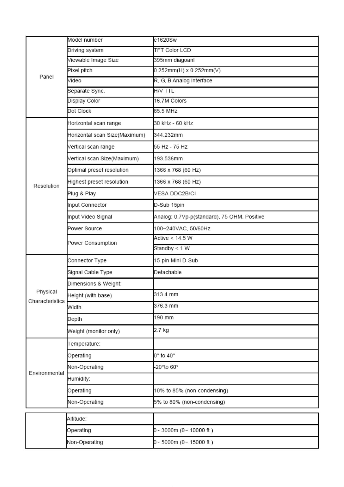
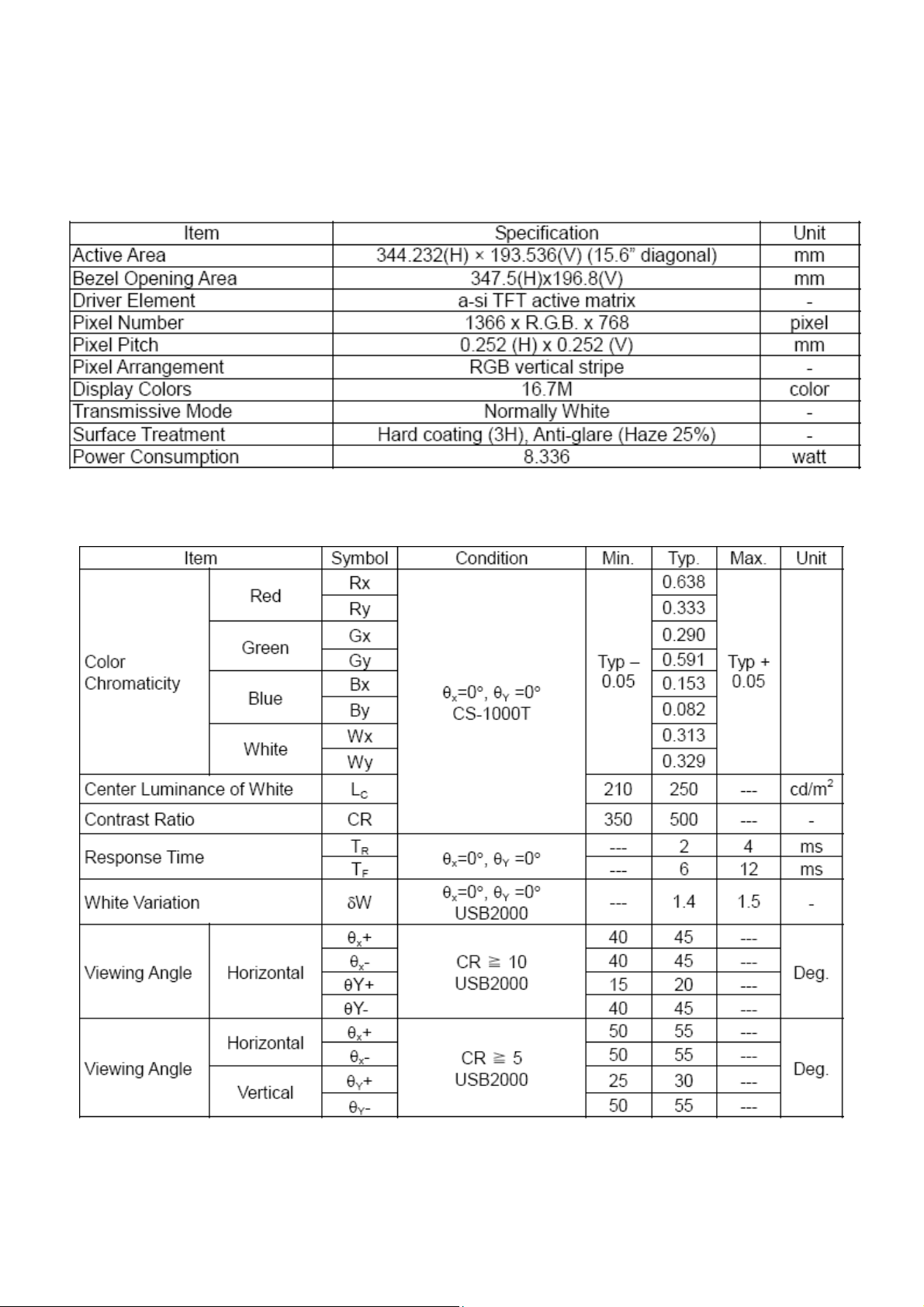
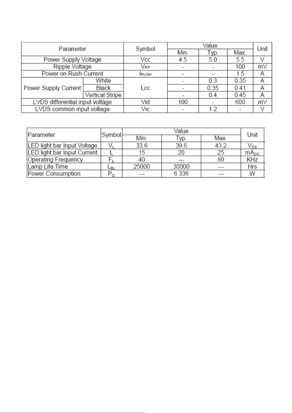
1. Monitor Specification
4
Page 5
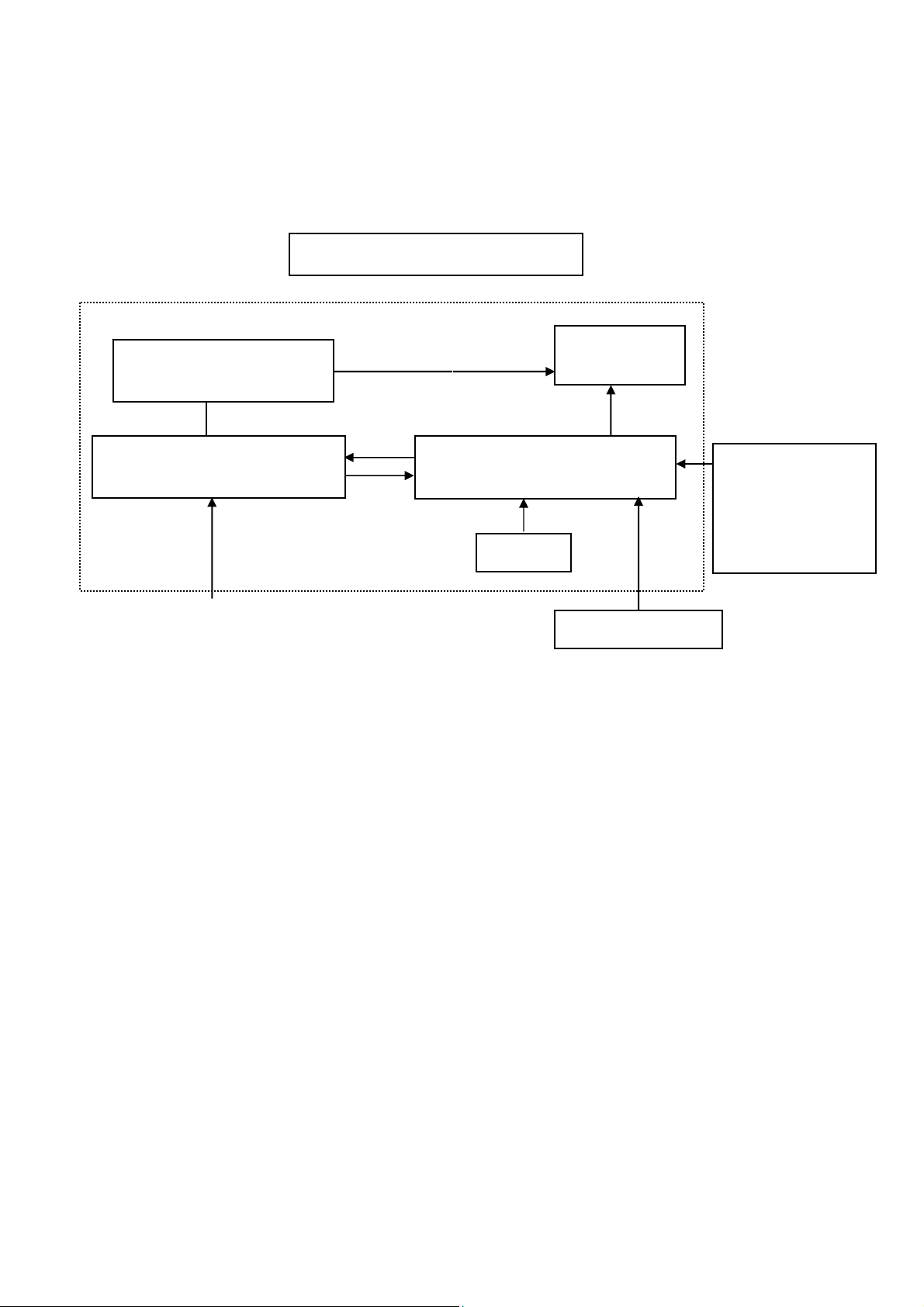
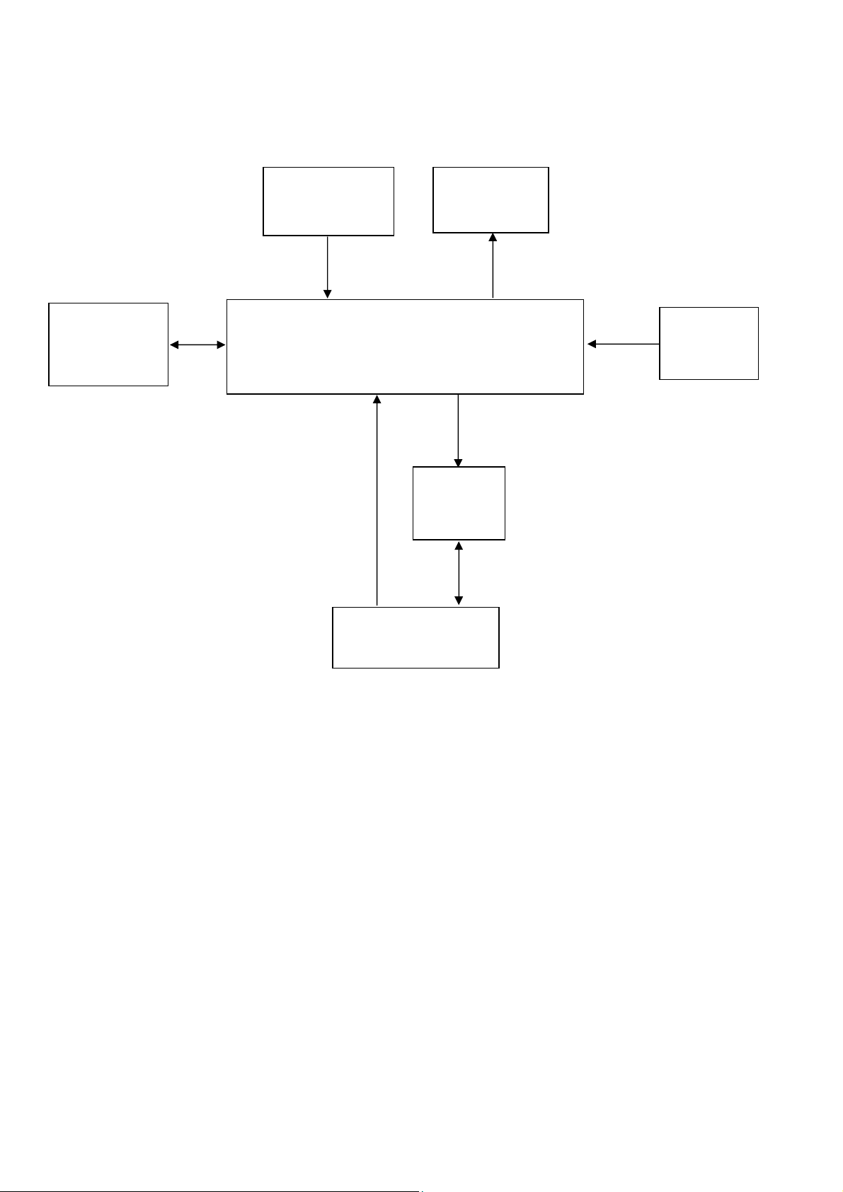
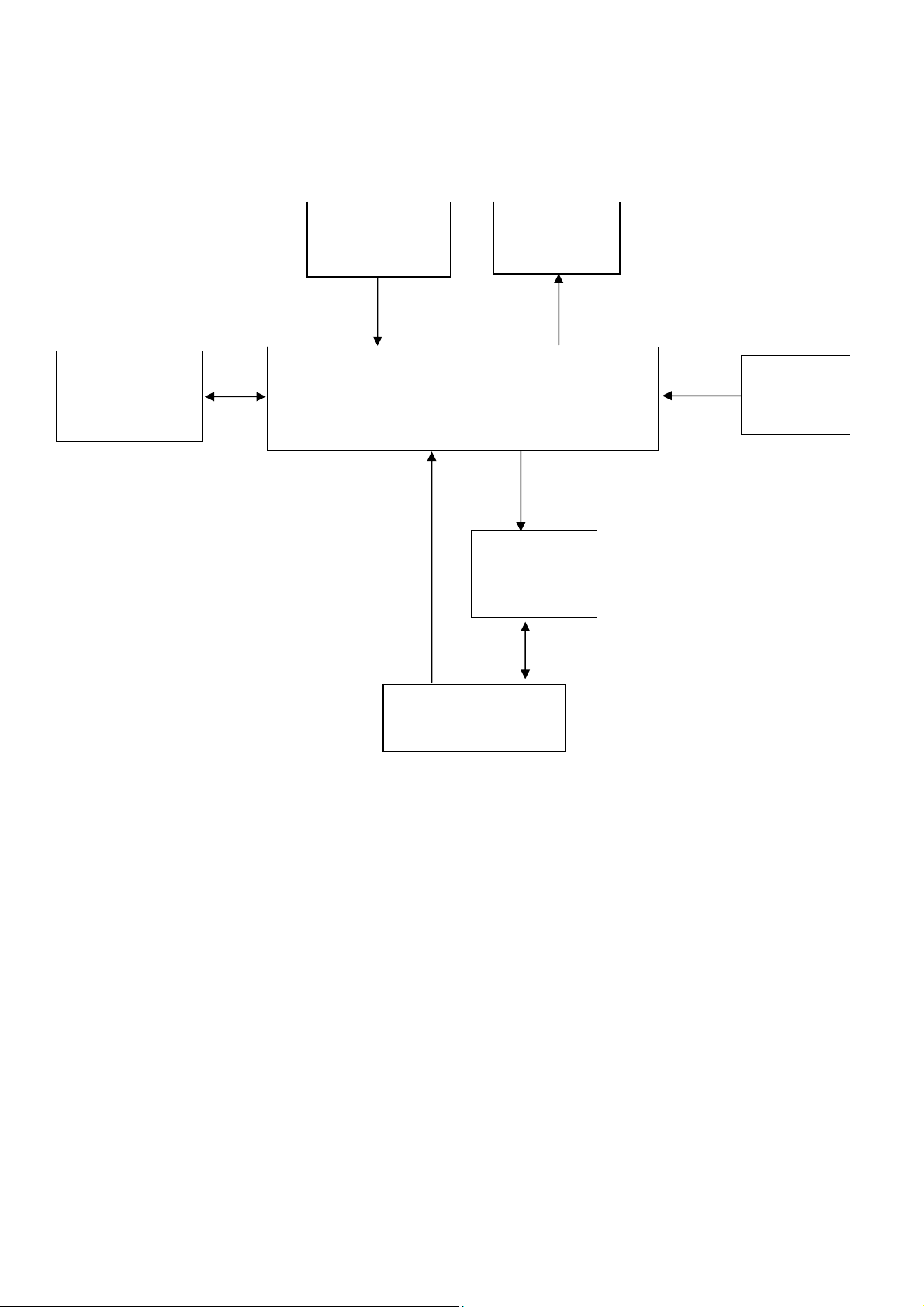
2. LCD Monitor Description
The LCD Monitor will contain a main board, an adapter board, a converter board and a key board which house the
flat panel control logic, brightness control logic and DDC.
The power board will provide AC to DC Inverter voltage to drive the backlight of panel and the main board chips
each voltage.
Converter Board
Adapter Board
AC-IN
100V~240V
Monitor Block Diagram
LED Drive.
Main Board
Key board
Flat Panel and
LED backlight
RS232 Connector
For white balance
adjustment in
factory mode
Video signal, DDC
HOST Computer
5
Page 6
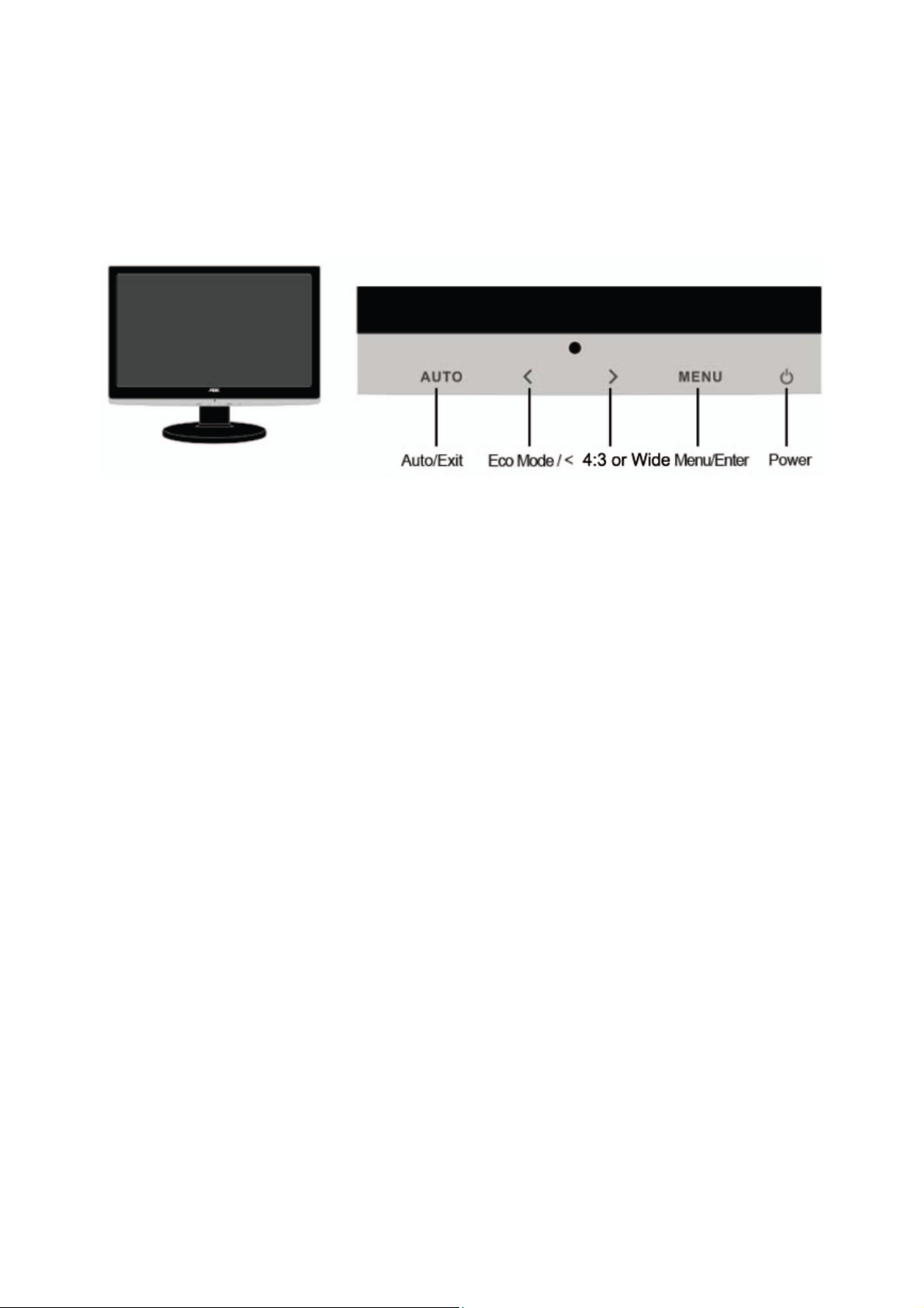
3. Operation Instructions
3.1 General Instructions
Press the power button to turn the monitor on or off. The other control knobs are located at front panel of the monitor.
By changing these settings, the picture can be adjusted to your personal preferences.
3.2 Control Buttons
Power
Press the Power button continuously to turn off the monitor.
4:3 or wide image ratio hot key
When there is no OSD, press > continuously to change 4:3 or wide image ratio. (If the product screen size is 4:3 or
input signal resolution is wide format, the hot key is disable to adjust. )
Eco Mode / <
Press the Eco key continuously to select the Eco mode of brightness when there is no OSD (Eco mode hot key
may not be available in all models).
Auto / Exit
When the OSD is closed, press Auto button will be auto configure hot key function.
6
Page 7

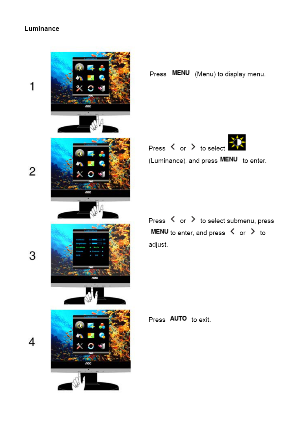
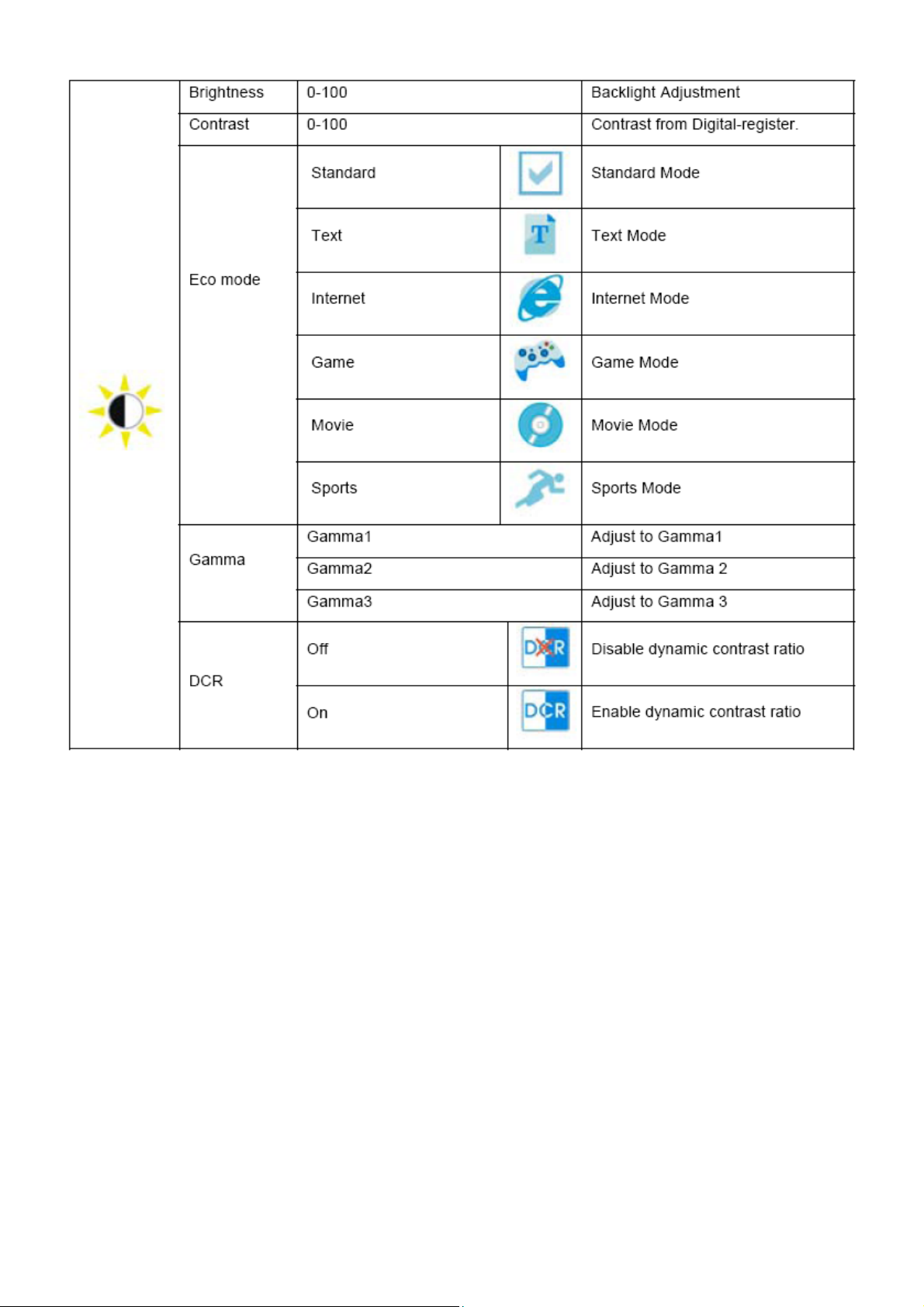
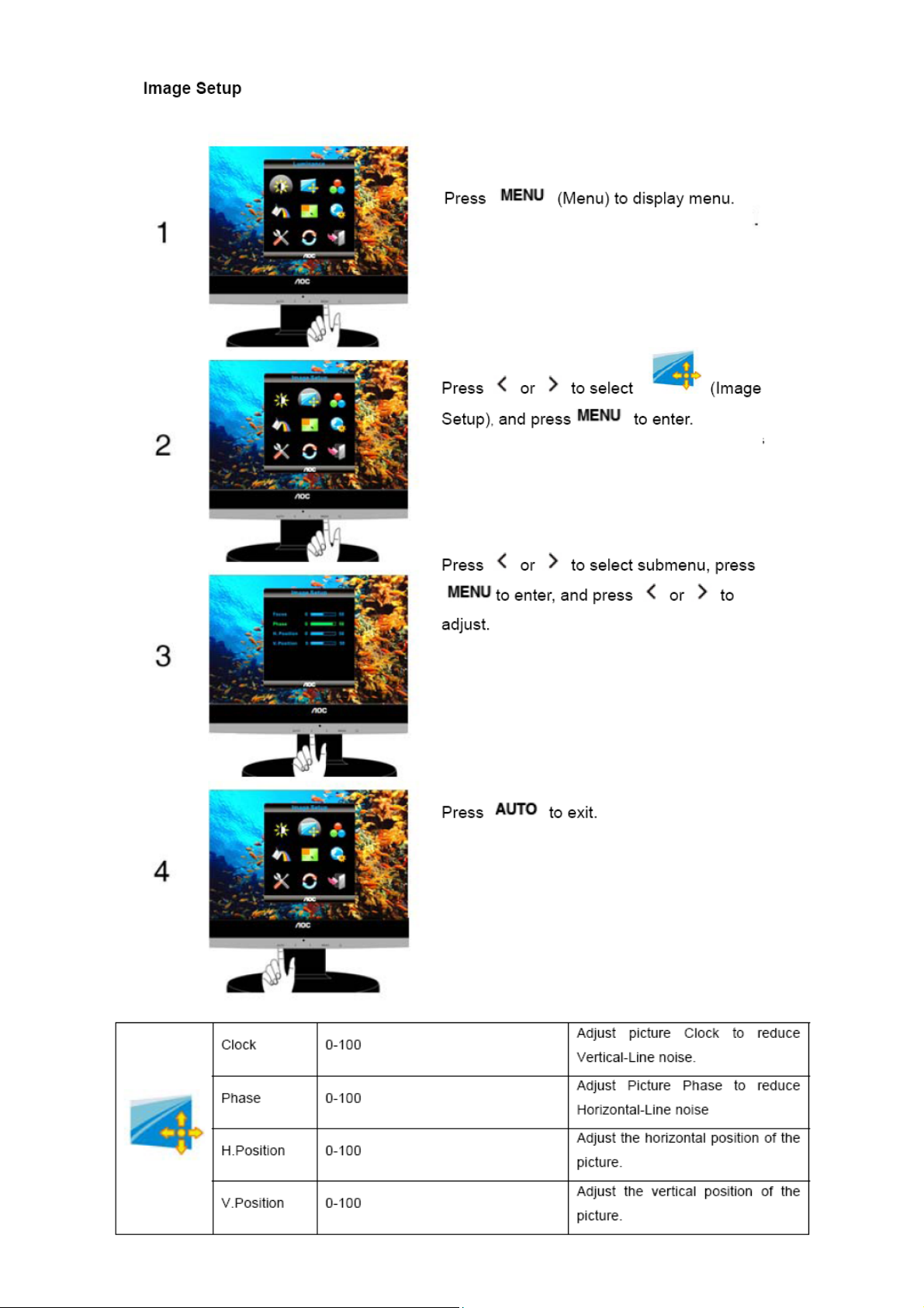
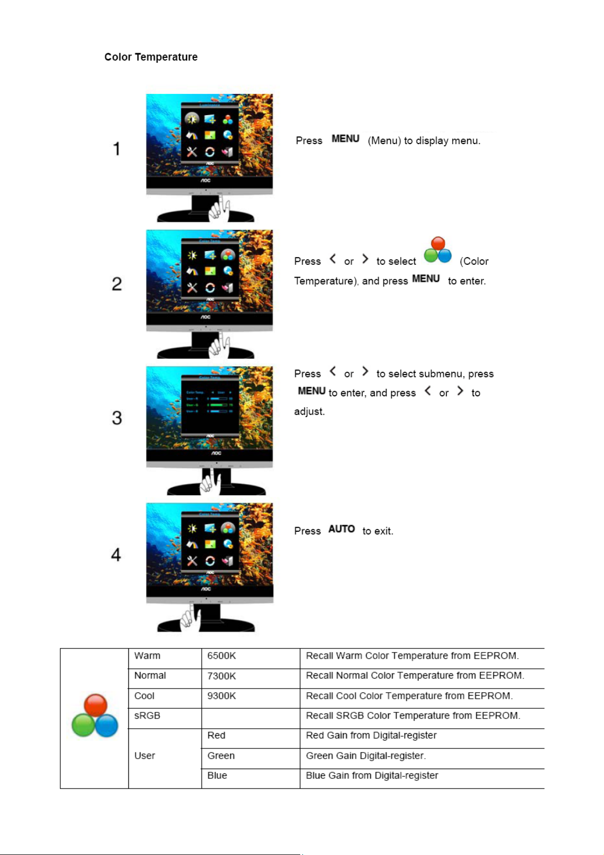
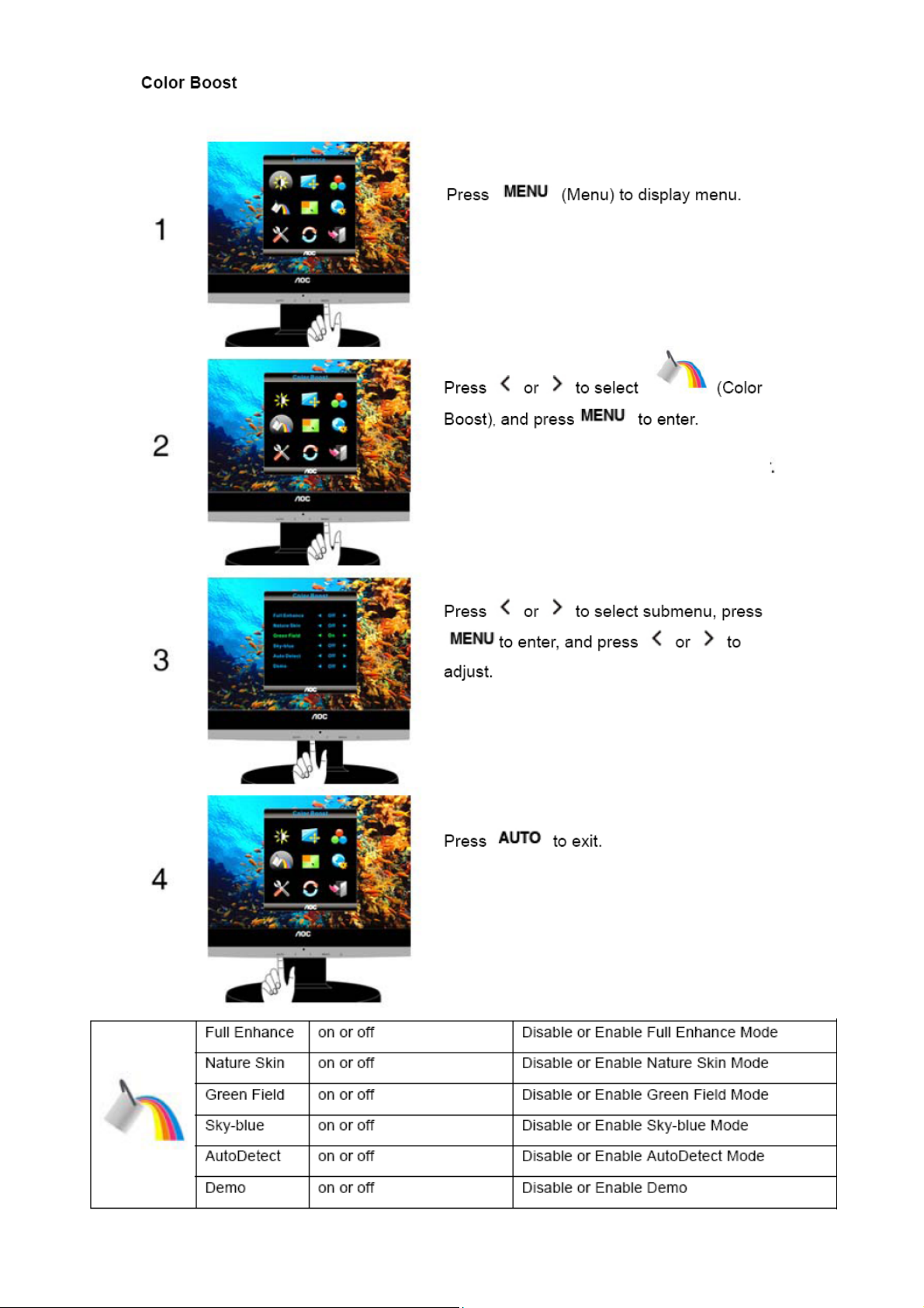
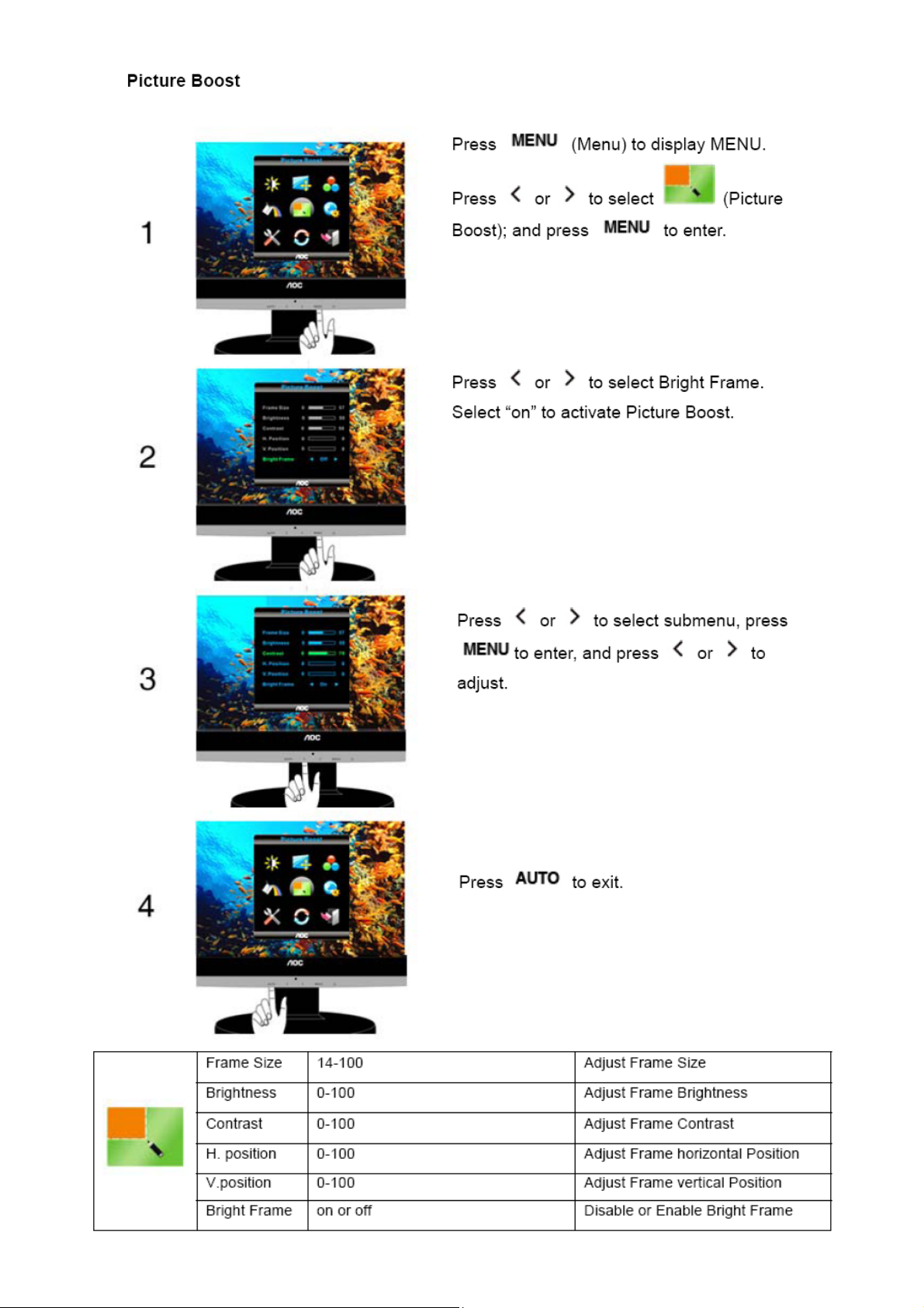
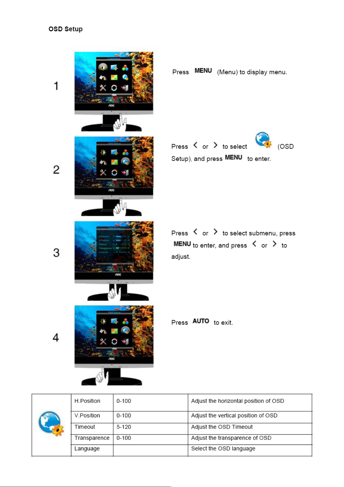
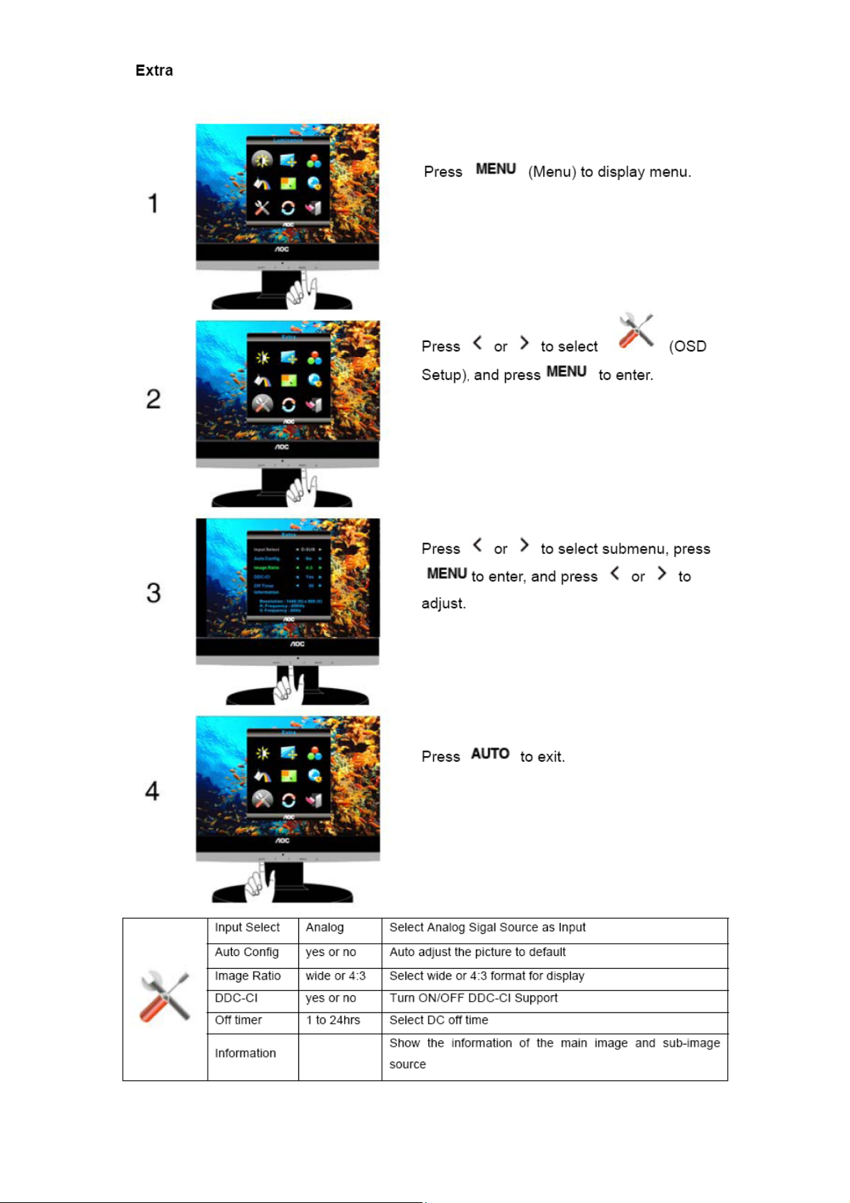
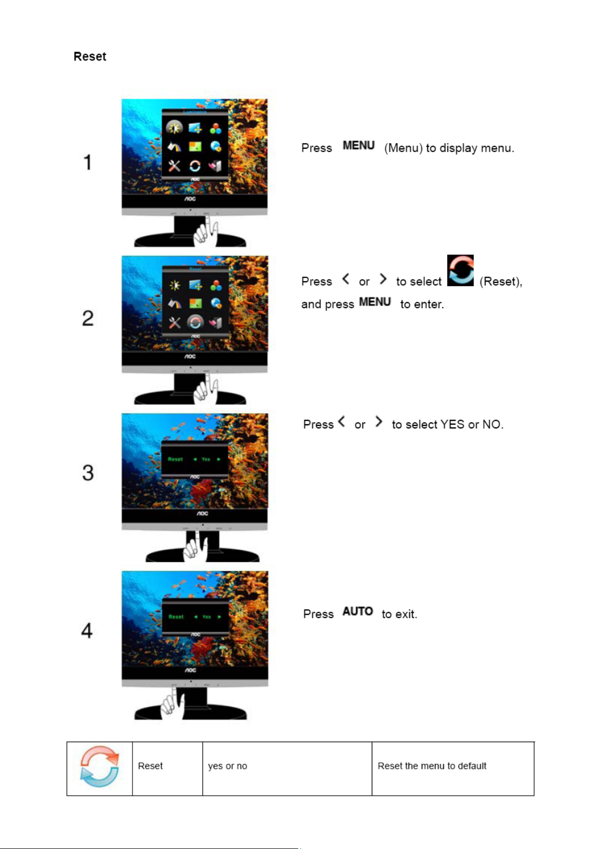
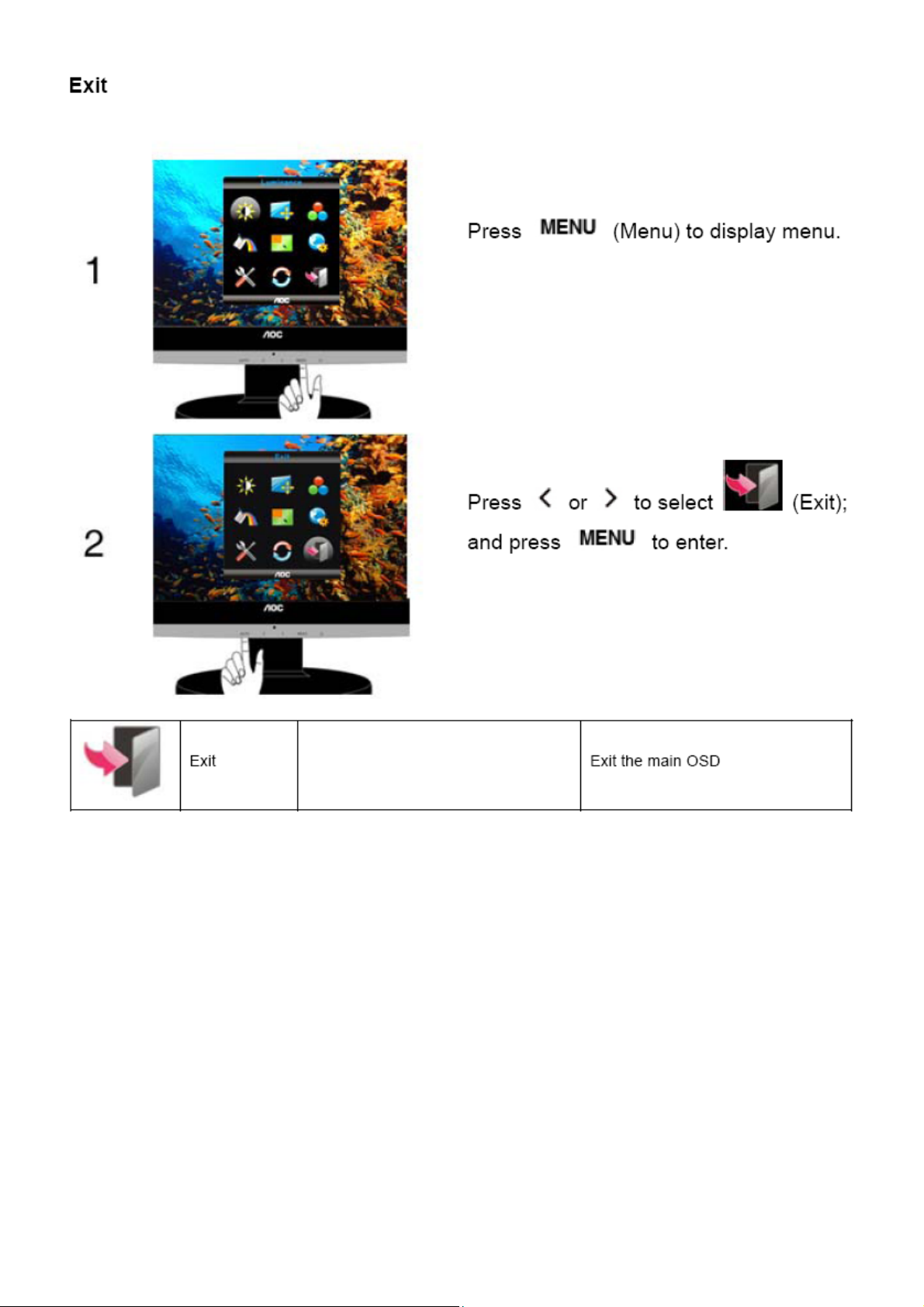
3.3 Adjusting the Picture
OSD Settings
1) Press the MENU-button to activate the OSD window.
2) Press < or > to navigate through the functions. Once the desired function is highlighted, press the MENU-button
to activate sub-menu . Once the desired function is highlighted, press MENU-button to activate it.
3) Press < or > to change the settings of the selected function. Press < or > to select another function in sub-menu.
Press AUTO to exit. If you want to adjust any other function, repeat steps 2-3.
4) OSD Lock Function: To lock the OSD, press and hold the MENU button while the monitor is off and then press
power button to turn the monitor on. To un-lock the OSD - press and hold the MENU button while the monitor is
off and then press power button to turn the monitor on.
Notes:
1) If the product has only one signal input, the item of "Input Select" is disable to adjust.
2) If the product screen size is 4:3 or input signal resolution is wide format, the item of "Image Ratio" is disable to
adjust.
3) One of DCR, Color Boost, and Picture Boost functions is active, the other two function is turned off accordingly.
7
Page 8
8
Page 9
9
Page 10
10
Page 11
11 12 13 14 15 16 17
Page 12
Page 13
Page 14
Page 15
Page 16
Page 17
Page 18
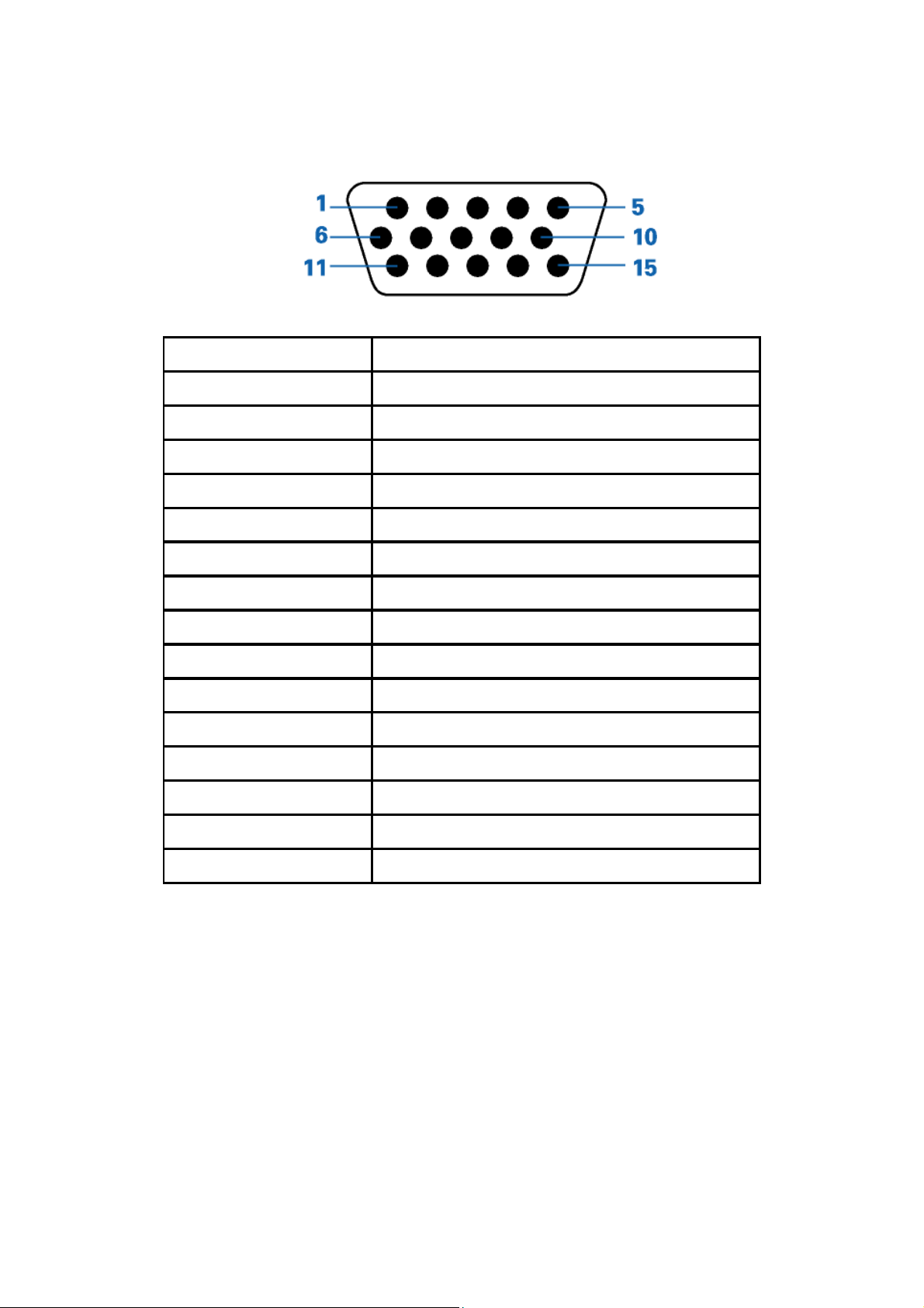
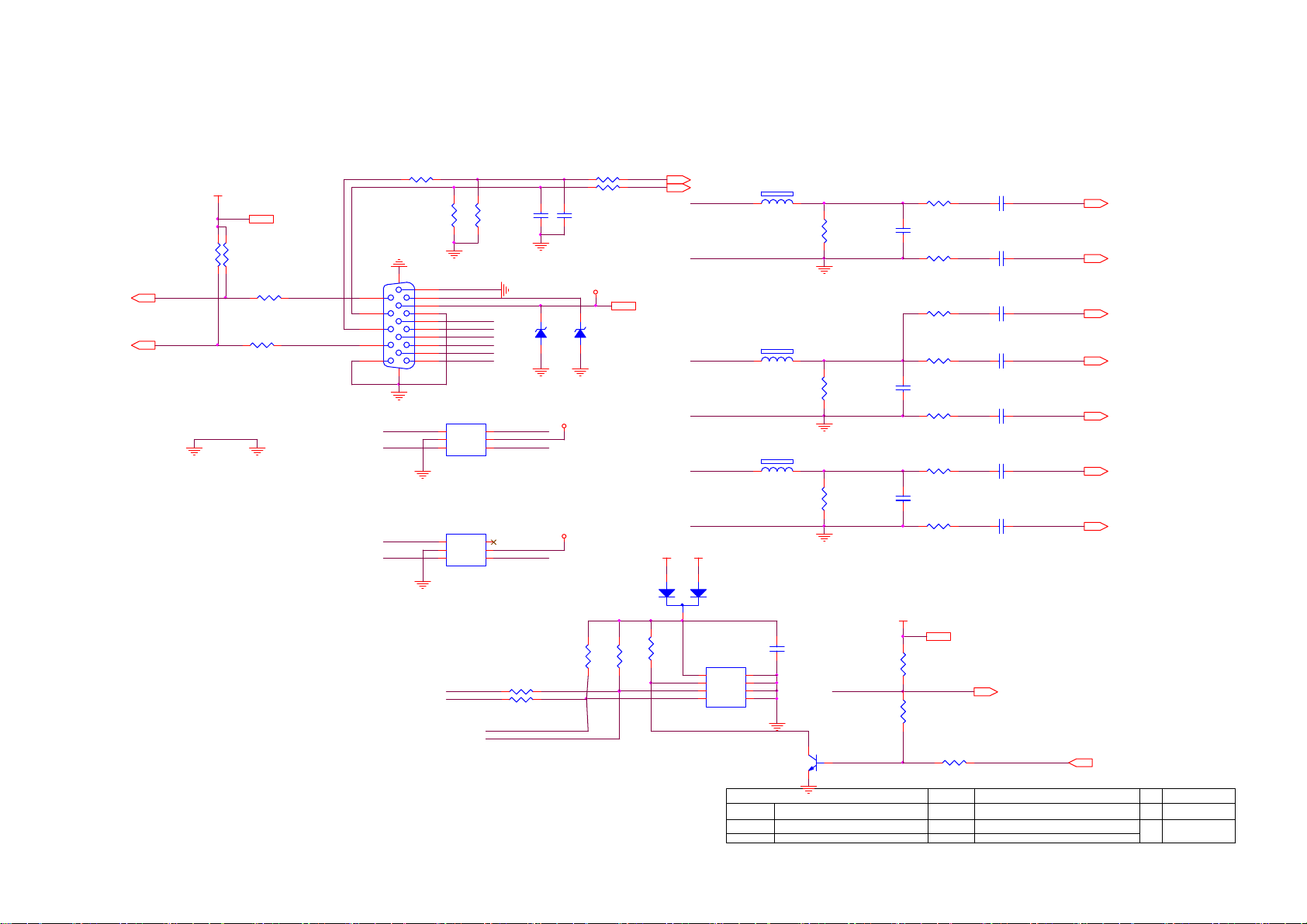
4. Input/Output Specification
4.1 Input Signal Connector
D-Sub 15pin Connector
Pin Number 15-Pin Side of the Signal Cable
1 Video-Red
2 Video-Green
3 Video-Blue
4 N.C.
5 Detect Cable
6 GND-R
7 GND-G
8 GND-B
9 +5V
10 Ground
11 N.C.
12 DDC-Serial data
13 H-sync
14 V-sync
15 DDC-Serial clock
18
Page 19
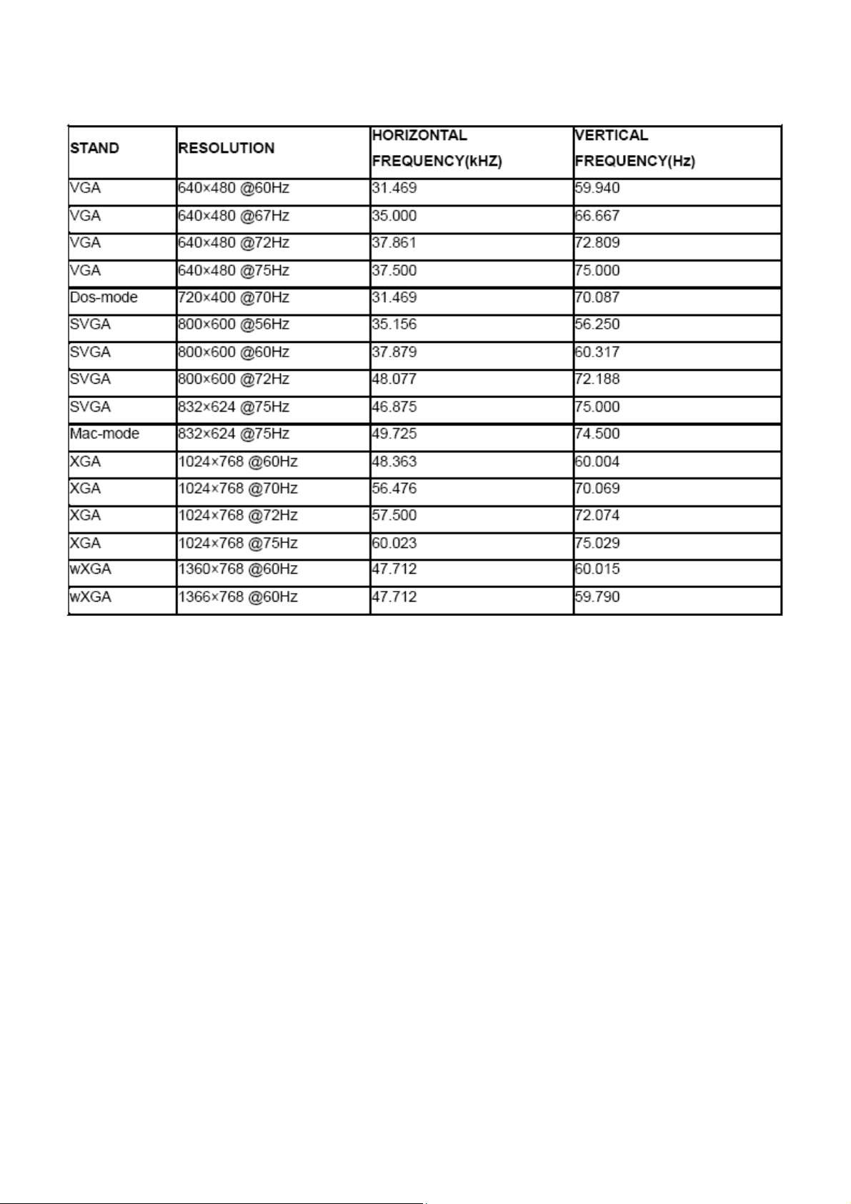
4.2 Factory Preset Display Modes
19
Page 20
4.3. Panel Specification
M156B1-L01 is a 15.6” wide TFT Liquid Crystal Display module with white LED(1PCS Lightbar, LED-3020 96PCS)
Backlight unit and 30pin 1ch-LVDS interface. This module supports 1366 x768 WXGA mode and can display up to
16.7M colors. The conventer module for Backlight is not built in.
4.3.1 General Feature
4.3.2 Optical Characteristics
20
Page 21
4.3.3 Electrical Characteristics
TFT LCD MODULE Ta = 25± 2 ºC
BACKLIGHT UNIT (LED matrix is 10S8P) Ta = 25 ± 2 ºC
21
Page 22
(
)
(
)
(
)
5. Block Diagram
5.1 Main board
Flash ROM
EN25F20
U402
14.31818MHZ
(X401)
Scalar TSUM1PFR-LF
(Include MCU, ADC, OSD)
(U401)
Panel Interface
(CN405)
EEPROM
M24C02
U405
Key Control
Interface
CN408
D-Sub Connector
(CN101)
22
Page 23
(
)
(
)
T6AMSP2EYHGGNN
715G3529 1
Flash ROM
MX25L2026DM1I
U402
14.31818MHZ
(X401)
Scalar TSUMU18NWR5-LF
(Include MCU, ADC, OSD)
(U401)
Panel Interface
(CN405)
EEPROM
FM24C02A
(U405)
Key Control
Interface
CN408
D-Sub Connector
(CN101)
23
Page 24
T6BMSR2EYHGGNN
715G4734M02000004I
XGA/SXGA LVDS OUTPUT
DSUB_5V
VCC3. 3
CMVCC1
VCC1.8
VCC3. 3
DSUB_5V
CMVCC
CMVCC1
02.Input
DSUB_5V
VCC3.3
CMVCC1
VCC1.8
VCC3.3
CMVCC
CMVCC1
DSUB_R+
DSUB_R-
DSUB_G+
DSUB_G-
DSUB_SOG
DSUB_B+
DSUB_B-
DSUB_H
DSUB_V
DDC1_SDA
DDC1_SCL
DET_CABLE
EDID _CTRL
PANEL_I D#DSUB_5V
VCTRL
DSUB_R+
DSUB_RDSUB_G+
DSUB_GDSUB_SOG
DSUB_B+
DSUB_BDSUB_H
DSUB_V
DDC1_SDA
DDC1_SCL
DET_CABLE
EDID _CTRL
PANEL_ID #
VCTRL
VCC1.8
VCC3.3
CMVCC
CMVCC1
PB[2. .9]
PPWR_ ON#
Adj_BACKLI GHT
on_BACKLI GHT
VCC1. 8
VCC3.3
PB[2. .9]
CMVCC
CMVCC1
CMVCC
CMVCC
PB[2. .9]
PPWR _ON#
Adj_BACKLI GHT
on_BACKLI GHT
05.Pow e r
03.Sca lar
04.Output
24
Page 25
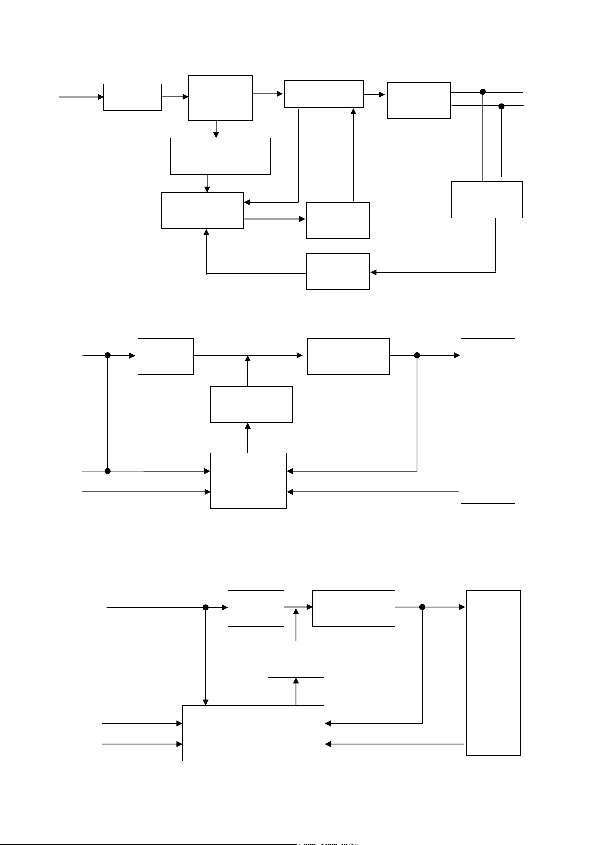
5.2 Power board
AC input
EMI filter
Bridge
Rectifier
and Filter
Transformer
Rectifier
diodes
12V
5V
Converter board
12V
DIM
ENA
Converter board
715G4013P01005004I
14.5V
Start Resistor
(R904,R932)
PWM Control
(IC901)
L801
MOSFET
(Q801)
PWM Control
TA9690GN
(IC801)
L801
Power Switch
Photo coupler
Q806
(Q901)
(IC902)
ZD801
D801
Feedback
Circuit
LED
(CN803)
LED
(CN803)
DIM
ON/OFF
PWM Control
MP3389EF
(U801)
25
Page 26
T6BMSR2EYHGGNN
715G3189P02LED001R
AC input
EMI filter
Bridge
Rectifier
and Filter
Start Resistor
(R920,R921,R922)
PWM Control
(IC901)
Transformer
Photo coupler
(IC902)
Rectifier
diodes
Feedback
Circuit
14.5V
5V
26
Page 27
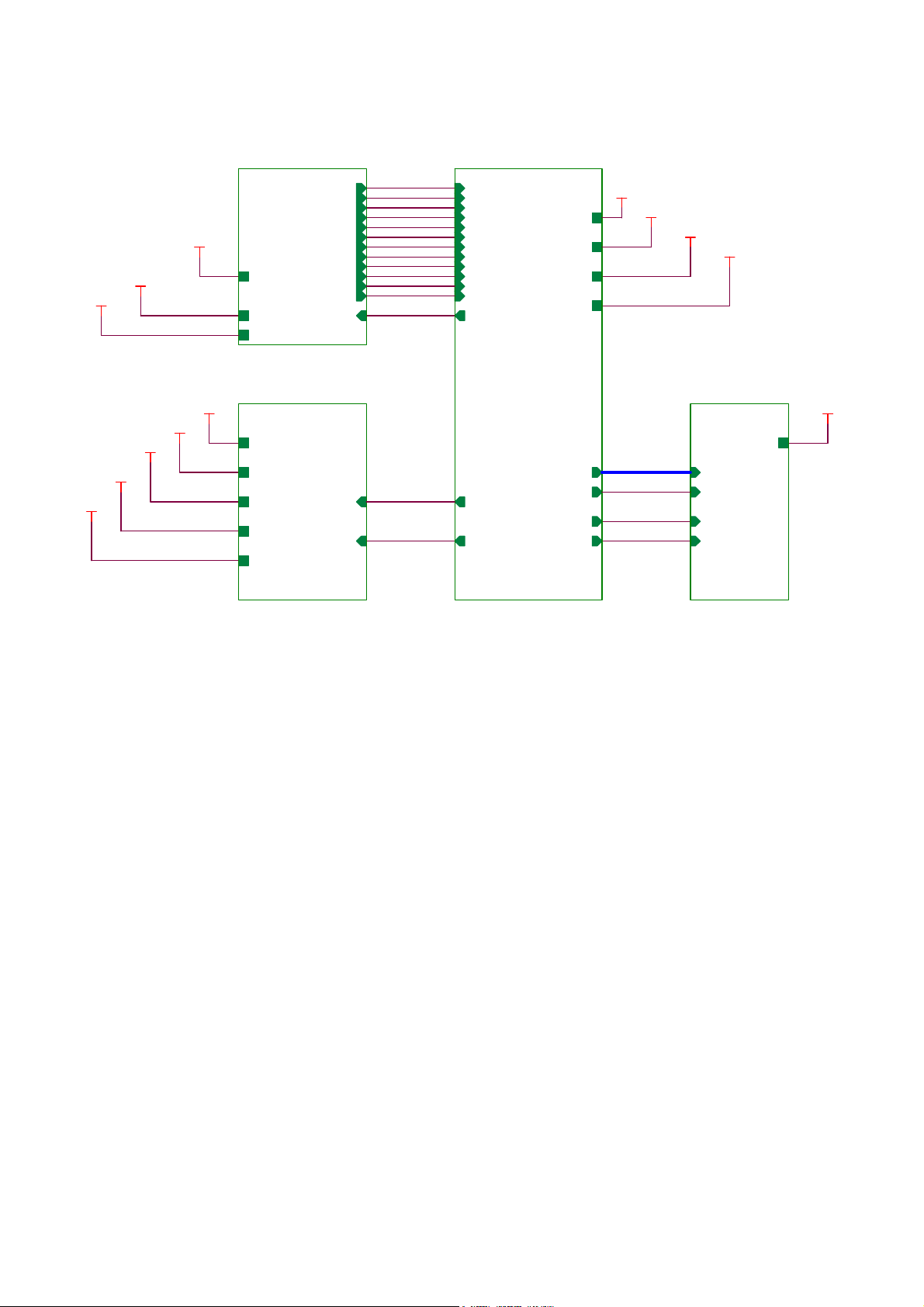
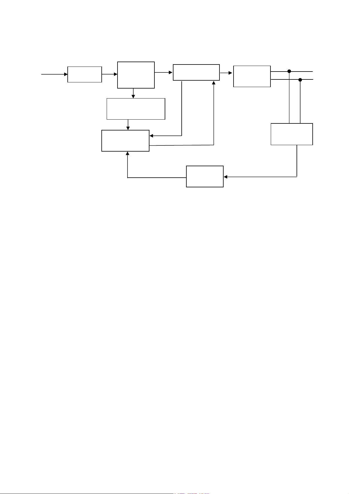
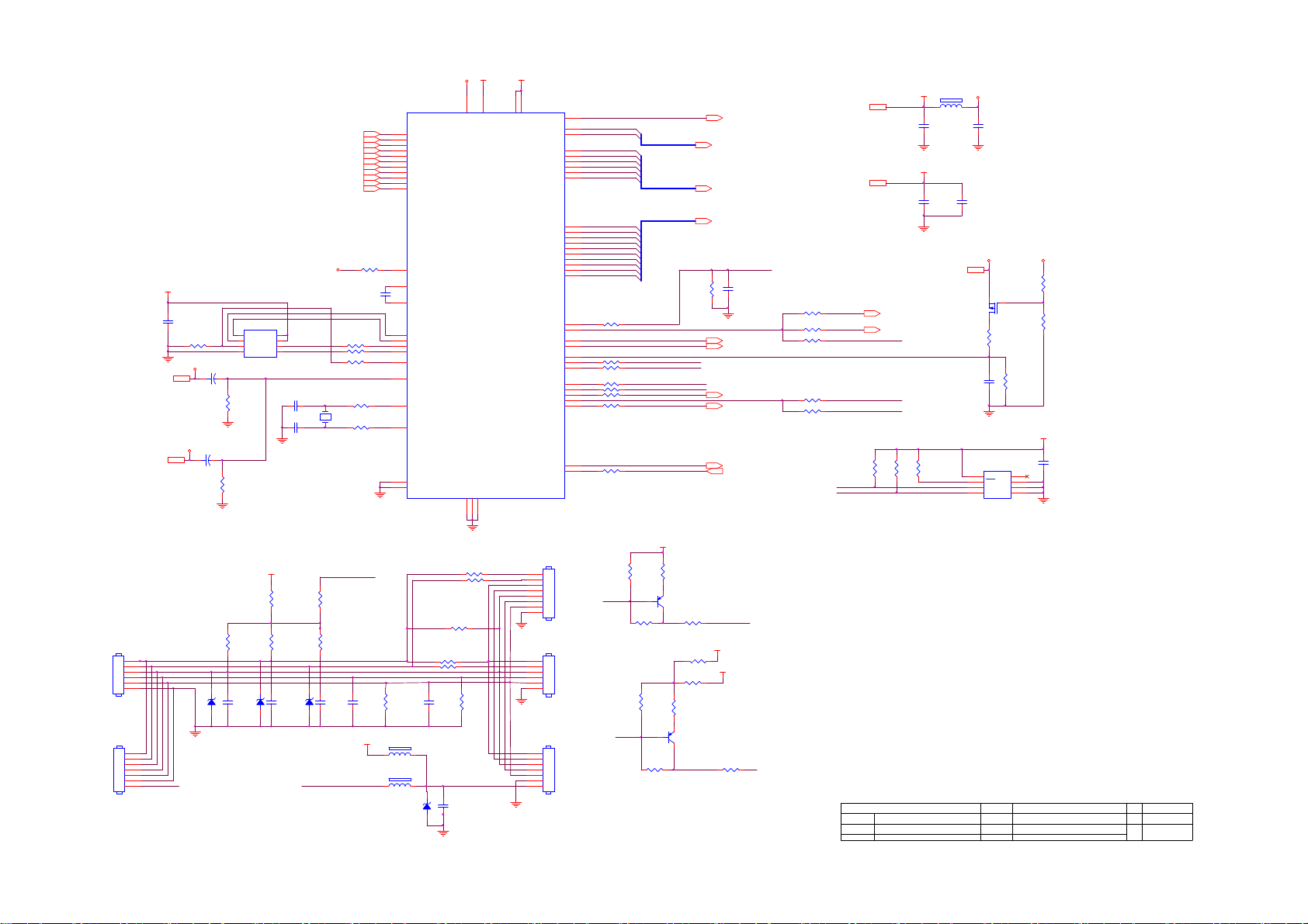
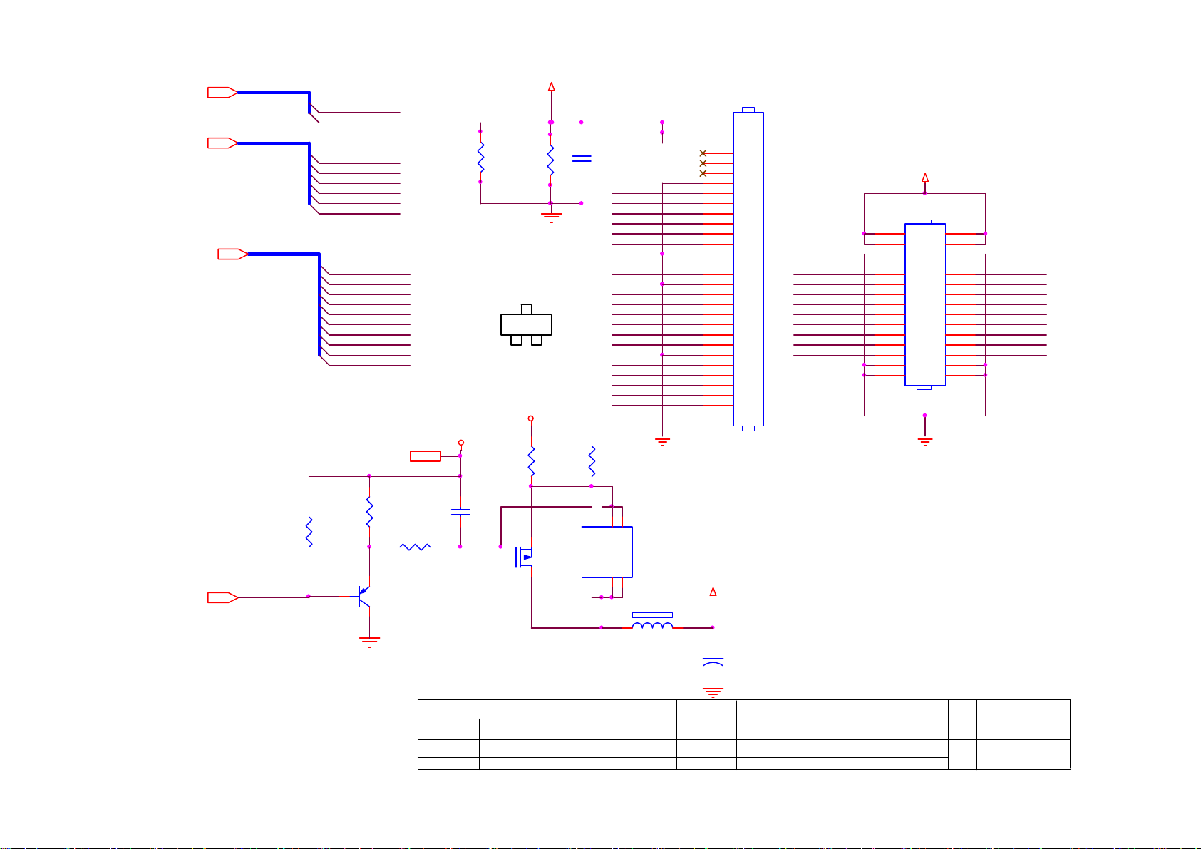
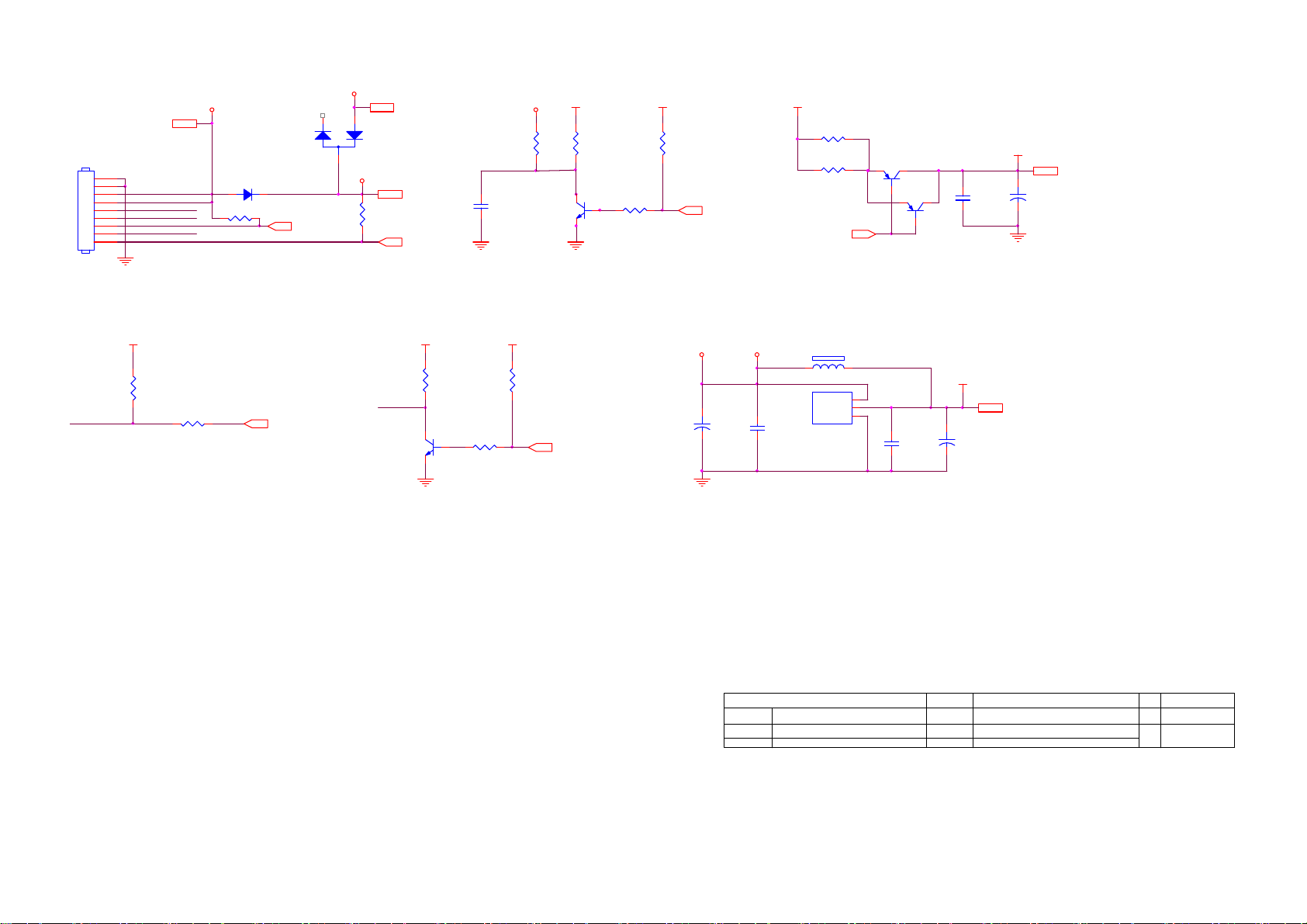
6. Schematic
6.1 Main Board
715G3529 1
VCC3. 3
R120
R121
NC
DDC1_SCL5
DDC1_SDA5
DDC1_SCL
DDC1_SDA
GND POWER DGND
NC
R113
NC
R110
NC
VCC3. 3 7
DSUB_SDA
DSUB_SCL
H_Sync
V_Sy nc
15
14
13
12
11
R101
0R05 1/ 10W 5%
2K2 1/16W 5%
CN101
DB15
17 16
DSUB_SDA
DSUB_SCL
VGA_G+
VGA_R+
R105
10
5
9
4
8
3
7
2
6
1
U103
AZC199-04 S
1
2
3 4
U102
AZC199-04 S
1
2
3 4
DSUB_SCL
DSUB_SDA
DSUB_5V
VGA_BVGA_B+
VGA_GVGA_G+
VGA_RVGA_R+
I/O1
I/O4
GND
VDD
I/O2 I/O3
I/O1
I/O4
GND
VDD
I/O2 I/O3
R106
2K2 1/16W 5%
6
5
6
5
DDC1_SDA
DDC1_SCL
C102
22pF
VGA_PLUG
ZD103
RLZ5.6B
ESD_VCC
H_Sync
V_Sy nc
ESD_VCC
VGA_B+
R475 47R 1/ 16W 5%
R476 47R 1/ 16W 5%
R102 100R 1/16W 5%
R103 100R 1/16W 5%
C103
22pF
DSUB_5V
ZD104
RLZ5.6B
ESD_VC C
R472
4.7K1/16W
DSUB_5V 5
CMVCC1
2
R474
R473
4.7K1/16W
DSUB_H 5
DSUB_V 5
VGA_B+
VGA_B-
VGA_G+
VGA_G-
VGA_R+
VGA_R-
DSUB_5V
1
3
4.7K1/16W
8
7
6
M24C02-WMN6TP
FB102
1 2
BEAD
R107
75R 1/16W 5%
FB103
1 2
BEAD
R112
75R 1/16W 5%
FB101
1 2
BEAD
R116
75R 1/16W 5%
D403
BAV70
U405
VCC
WP
SCL
A0
A1
A2
VSSSDA
LMBT3904LT1G
絬 隔 瓜 絪 腹
Key Component
C434
0.22uF16V
1
2
3
45
Q407
T P V ( Top Victory Electronic s Co . , Ltd. )
G3529-1-X-X-4-090725
02.Input
Date
VGA_PLUG
CMVCC1
R104
100R 1/16W 5%
C104
5pF/50V
R108
100R 1/16W 5%
R109
390 OHM 1/16W
R111
100R 1/16W 5%
C108
5pF/50V
R114
100R 1/16W 5%
R115
100R 1/16W 5%
C111
5pF/50V
R117
100R 1/ 16W 5%
CMVCC1 5
R118
10K 1/16W 5%
R122
NC
R123
4.7K1/16W
OEM MODEL Size
TPV MOD EL
PCB NAME
Sheet
C101
47N16V
C105
47N16V
C106
47N16V
C107
47N16V
C109
47N16V
C110
47N16V
C113
47N16V
DET_CABLE 5
715G3529-1
of
47Friday , January 15, 2010
EDID _CTRL 5
DSUB_B+ 5
DSUB_B- 5
DSUB_SOG 5
DSUB_G+ 5
DSUB_G- 5
DSUB_R+ 5
DSUB_R- 5
Rev
称爹
B
F
称爹
>
<
27
Page 28
VCC3.3
AVDD
U401
0.1uF/16V
R401
R402
13
RIN0P
12
RIN0M
10
GIN0P
9
GIN0M
11
SOGIN0
8
BIN0P
7
BIN0M
16
HSYNC0
17
VSYNC 0
18
DDCA_SD A/RS232_TX
19
DDCA_SC L/rs232_RX
4
REXT
15
REFP
C401
14
REFM
21
SDO
22
SCZ
23
SCK
24
SDI
28
GPIO_P27/PWM1
54
RST
1
XIN
2
XOU T
31
MODE [0]
32
MODE [1]
DSUB_R+3
DSUB_R-3
DSUB_G+3
DSUB_G-3
DSUB_SOG3
DSUB_B+3
DSUB_B-3
DSUB_H3
DSUB_V3
DDC1_SDA3
DDC1_SCL3 PA[4..9] 5
AVDD
VCC3.3
C408
220N 10V
R408
10K 1/16W 5%
CMVCC1
CMVCC17
CMVCC7
CMVCC
NC
10UF50V
C430
+
C410
+
U402
1
CE#
VDD
2
SO
HOLD#
WP
3
WP#
SCK
4 5
VSS SI
IC EN25F 20-100GIP 2Mb SOP-8
R417
10K 1/16W 5%
R460
NC
8
7
6
C411 47pF
C412 47pF
R403 390 OHM 1/16W
R456 33 OHM 1/16W
R457 33 OHM 1/16W
R405 100R 1/16W 5%
0R05 1/16W
X40 1
14.31818MHz
0R05 1/16W
1 2
6
51
VDDP
AVDD_ADC
LVDS
GND
GND
GND
5
29573
TSUM1PFR-LF
VCC1.8
30
53
VDDC
VDDC
LVBCKP
LVBCKM
GPIO_P15/PWM0
PWM2/GPIO_P24
GPIO_P12
PWM1/GPIO_P25
GPIO_P00/SAR1
GPIO_P01/SAR2
GPIO_P06
GPIO_P07
PWM0/GPIO_P26
GPIO_P13
GPIO_P14
GPIO_P10/I2C _MCL
GPIO_P11/I2C _MDA
VCTRL
LVA3P
LVA3M
LVA2P
LVA2M
LVA1P
LVA1M
LVA0P
LVA0M
LVB3P
LVB3M
LVB2P
LVB2M
LVB1P
LVB1M
LVB0P
LVB0M
RSTN
52
33
34
35
36
37
38
39
40
41
42
43
44
45
46
47
48
49
50
20
R424 NC
27
55
56
58
R411 100R 1/ 16W 5%
59
R412 100R 1/16W 5%
60
R414 10K1/16W
61
R410 3.9K 1/16W
62
R418 100R 1/16W 5%
63
64
R419 100R 1/16W 5%
26
25
R413 100R 1/ 16W 5%
EDID_C TRL 3
PANEL_ID# 7
R454
R453
NC
NC
VCC3.3
VCC1.8
R455
NC
VCC3.37
VCC1.87
R487
0R011/16W
MSDA
POWER_KEY #
MSCL
MSCL
MSDA
LED_G/B
LED_O
R425
NC
VCTRL 7
PA[0..1] 5
PB[0..9] 5
C418
NC
on_BACKLIGHT 7
adj_BACKLIGHT 7
Volume# 7
Mute 7
PPWR_ON# 6
DET_CABLE 4
EE_WP
R426 NC
R452 NC
R420 100OHM1/16W
R451 NC
PA0
PA1
PA4
PA5
PA6
PA7
PA8
PA9
PB0
PB1
PB2
PB3
PB4
PB5
PB6
PB7
PB8
PB9
PA[0..1]
PA[4..9]
PB[0..9]
KEY2
KEY1
FB401
300OHM
C403
0.1uF/16V
C406
0.1uF/16V
EE_WP
CMVCC7
NC
AVDD
C407
0.1uF/16V
Q401
NC
C409
C404
0.1uF/16V
CMVCC
R406
NC
R409
NC
U403
8
VCC
NC
7
E1
WC
6
E2
SCL
VSSSDA
NC/M24C04-W MN6TP
CMVCC1
R458
NC
R459
NC
VCC3.3
C429
NC
1
2
3
45
CN408
CONN
CN409
NC/CONN
6
5
4
3
2
1
I2C_SCL
7
I2C_SDA
6
5
INT
LED Power
4
3
2
1
TOUCH_POWER
3.9K 1/16W
ZD404
NC/U DZSNP5.6B
R421
1 2
R483
0R05 1/16W
R427
3.9K OHM 1/16W
C413
NC
ZD402
NC/UDZSNP5.6B
VCC3.3
1 2
C414
NC
ZD403
NC/UDZSNP5.6B
LED_ORANGE/TOUCH_VCC
LED_ORANGE/TOUC H_VCC
R484
NC
R428
3.9K OHM 1/16W
KEY1
KEY2
POWER_KEY#
LED_GRN/ BLUE
LED_ORANGE/TOUC H_VCC
C415
NC
1 2
C416
0.1uF/16V
VCC3.3
R404
NC
FB404
NC
FB405
150 OHM
ZD401
NC/U DZSNP5.6B
R463
R464 2K OHM 1/16W
R478 NC
R461
1K 1/16W 5%
R462 1K 1/16W 5%
C417
100N 16V
TOUCH_POWER
C433
1uF 10V
1 2
2K OHM 1/16W
R407
10K 1/16W 5%
I2C_SCL
I2C_SDA
INT
LED Power
CN406
1
2
3
4
5
6
7
8
NC/CONN
CN402
1
2
3
4
5
6
NC/CONN
CN407
1
2
3
4
5
6
7
NC/CONN
R466
2.2K1/16W
LED_G/B
1K1/16W
R469
LED_O
1
R488
NC
R489
NC
28
CMVCC1
R467
0R011/16W
23
2N3906S-RTK/PS
Q403
R468 200 OHM +-5% 1/16W
R481
NC
R482 0R05OHM1/16W
R470
0R011/16W
Q402
2N3906S-RTK/PS
LED_GRN/BLUE
CMVCC1
VCC3.3
LED_ORANGE/TOUC H_VCC
R471 0R011/16W
T P V ( Top Victory Electronics Co . , Ltd. )
G3529-1-X-X-4-090725
絬 隔 瓜 絪 腹
Key Component
03.Scalar
Date
OEM MODEL Size
TPV MODEL
PCB NAME
715G3529-1
Sheet
of
57Tuesday, Novemb er 10, 2009
C
Rev
F
称爹
>
<
称爹
Page 29
R477
1
G
AO3401L
CMVCC
0 OHM +-5% 1/4W
PANEL_VCC
R434
330OHM1/4W
3
D
2
S
R485
Q405
AO3401
C420
0.1uF/16V
PA0
PA1
PB2
PB3
PA4
PA5
PA6
PA7
PA8
PA9
PB0
PB1
PB2
PB3 PB6
PB4
PB5
PB6
PB7
PB8
VCC3.3
PB9
R486
0 OHM +-5% 1/4W(N C)
123
4
SSS
G
DDD
D
876
5
Q411
NC/AO4411
FB402
1
2
3
4
5
6
7
8
9
10
11
12
13
14
15
16
17
18
19
20
21
22
23
24
25
26
27
28
29
30
PANEL_VCC
CN403
NC/CONN
PA1
PB3
PA5
PA7
PA9
PB1
PB3
PB5
PB7
PB9
PANEL_VCC
CN405
1
3
5
7
9
11
13
15
17
19
21
23
25
27
29
CONN
2
4
6
8
10
12
14
16
18
20
22
24
26
28
30
PA0
PB2
PA4
PA6
PA8
PB0
PB2
PB4
PB8
PA[0..1]5
PA[4..9]5
PB[0. .9]5
PPWR_ON#5
PA[0..1]
PA[4..9]
PB[0. .9]
PA0
PA1
PA4
PA5
PA6
PA7
PA8
PA9
R435
4K7 1/16W 5%
1
PPWR_ON#
7
PB0
PB1
PB2
PB3
PB4
PB5
PB6
PB7
PB8
PB9
23
CMVCC
R433
10K 1/16W 5%
R436
100K 1/16W 5%
PMBS3906
Q404
CMVCC
NC
C419
0.1uF/16V
T P V ( Top Victory Elect ronics Co . , Ltd. )
絬 隔 瓜 絪 腹
Key Component
Date
G3529-1-X-X-4-090725
04.Out put
29
120OHM
C421
+
100uF16V
OEM MODEL Size
TPV MODEL
PCB NAME
Sheet
715G3529-1
of
67Monday, J uly 27, 2009
Rev
称爹
<
A
F
称爹
>
Page 30
DSUB_5V
CMVCC1
R465
NC
Q406
VCC3.3
R437
10K 1/16W 5%
VCC3. 3
R440
4K7 1/16W 5%
R439
10K 1/16W 5%
on_BACKLIGH T 5
VCC3. 3
R480
2.2 OHM +-5% 2WS
R479
NC
VCTRL5
Q410
KN2907AS
Q409
KN2907AS
C432
0.1uF/16V
VCC1. 8
+
C423
100uF16V
VCC1. 8 5
CN404
CONN
9
8
7
6
5
4
3
2
1
CMVCC5, 6
CMVCC
CMVCC
BKLT-VBRI
BKLT-EN
C_PANEL_I NDEX
Volume
Mut e
CMVCC
SM340A
D402
R450 NC
NC(R 0402)
2
3
PANEL_ID # 5
1
CMVCC1
D401
BAV99
R449
NC
DSUB_5V 2
CMVCC1 5
Mut e 5
BKLT-EN
C425
NC
2N3904S-RTK/PS
BKLT-VBRI
VCC3. 3
R441
1K 1/16W 5%
100R 1/16 W 5%
R442
adj_BACKLIGH T 5
Volume
VCC3. 3
R446
NC
Q408
2N3904S-RTK/PS
VCC3. 3
R448
4K7 1/16W 5%
R447
10K 1/16W 5%
Volume# 5
CMVCC1
+
MVC C
C426
100uF16V
T P V ( Top Victory Electronics Co . , Ltd. )
絬 隔 瓜 絪 腹
Key Component
Date
FB403 NC
C428
0.1uF/ 16V
G3529-1-X-X-4-090725
05.Power
VIN
VOUT
ADJ(GN D)
U404
AP1117D33L-13
VCC3. 3
3
2
1
C422
0.1uF/16V
+
OEM MODEL Size
TPV MODEL
PCB NAME
Sheet
C427
100uF16V
715G3529-1
77Monday , July 27, 2009
VCC3.3 4, 5
of
Rev
称爹
B
F
称爹
>
<
30
Page 31

T6AMSP2EYHGGNN
715G3529 1
VCC3.3
R120
NC
DDC1_SCL5
DDC1_SDA5
DDC1_SCL
DDC1_SDA DSUB_SDA
GND POWER
R121
NC
R113
NC
R110
NC
DGND
R101
0R05 1/10W 5%
H_Sync
V_Sy nc
DSUB_5V
VGA_BVGA_B+
VGA_GVGA_G+
VGA_RVGA_R+
U103
AZC199 -04S
I/O1
I/O4
GND
VDD
I/O23I/O3
U102
AZC199 -04S
I/O1
I/O4
GND
VDD
I/O23I/O3
DSUB_SCL
DSUB_SDA
R106
2K2 1/16W 5%
6
5
4
6
5
4
R475 47R 1/ 16W 5%
R476 47R 1/ 16W 5%
DDC1_SDA
DDC1_SCL
R105
15
14
13
12
11
DSUB_SDA
DSUB_SCL
VGA_G+
2K2 1/16W 5%
CN101
10
5
9
4
8
3
7
2
6
1
DB15
17 16
1
2
1
2
VCC3.3 7
DSUB_SCL VGA_PLUG
ZD103
RLZ5.6B
H_Sync
V_Sy nc
VGA_B+VGA_R+
C102
22pF
ESD_VCC
ESD_VCC
R102 100R 1/16W 5%
R103 100R 1/16W 5%
C103
22pF
DSUB_5V
ZD104
RLZ5.6B
ESD_VC C
R472
4.7K1/ 16W
DSUB_5V 5
CMVCC1
2
R474
R473
4.7K1/ 16W
DSUB_H 5
DSUB_V 5
VGA_B+
VGA_B-
VGA_G+
VGA_G-
VGA_R+
VGA_R-
DSUB_5V
1
3
4.7K1/16W
8
7
6
5
FM24C02A-SO-T-G
FB102
1 2
BEAD
FB103
1 2
BEAD
FB101
1 2
BEAD
D403
BAV70
U405
1
A0
VCC
2
A1
WP
3
A2
SCL
4
VSS
SDA
LMBT3904LT1G
絬 隔 瓜 絪 腹
Key Component
Q407
T P V ( Top Victory Electronics Co . , Ltd. )
G3529-1-X-X-5-100420
02.Inpu t
Date
C434
0.22uF16V
R107
75R 1/16W 5%
R112
75R 1/16W 5%
R116
75R 1/16W 5%
VGA_PLUG
CMVCC1
R104
100R 1/16 W 5%
C104
5pF/50V
R108
100R 1/16 W 5%
R109
390 OHM 1/16W
R111
100R 1/16 W 5%
C108
5pF/50V
R114
100R 1/16 W 5%
R115
100R 1/16 W 5%
C111
5pF/50V
R117
100R 1/16 W 5%
CMVCC1 5
R118
10K 1/16W 5%
R122
NC
R123
4.7K1/1 6W
OEM MO DE L
TPV MODEL
PCB NAME
Sheet
C101
47N16V
C105
47N16V
C106
47N16V
C107
47N16V
C109
47N16V
C110
47N16V
C113
47N16V
DET_CABLE 5
715G3529-1
47Wednes day , Augus t 04, 20 10
of
DSUB_B+ 5
DSUB_B- 5
DSUB_SOG 5
DSUB_G+ 5
DSUB_G- 5
DSUB_R+ 5
DSUB_R- 5
EDID _CTRL 5
Size
Rev
称爹
B
F
<
称爹
>
31
Page 32

VCC3.3 VCC1. 8
AVDD
U401
R403 390 OH M 1/16W
C401
0.1uF/16V
R401
R402
13
RIN0P
12
RIN0M
10
GIN0P
9
GIN0M
11
SOGIN0
8
BIN0P
7
BIN0M
16
HSYNC0
17
VSYN C0
18
DDCA_SDA /RS232_TX
19
DDCA_SCL/ rs232_RX
4
REXT
15
REFP
14
REFM
21
SDO
22
SCZ
23
SCK
24
SDI
28
GPIO_P27/PWM1
54
RST
1
XIN
2
XOU T
31
MODE [0]
32
MODE [1]
DSUB_R+3
DSUB_R-3
DSUB_G+3
DSUB_G-3
DSUB_SOG3
DSUB_B+3
DSUB_B-3
DSUB_H3
DSUB_V3
DDC1_SDA3
DDC1_SCL3
AVDD
VCC3.3
C408
220N 10V
R408
10K 1/16W 5%
CMVCC1
CMVCC17
10UF50V
CMVCC
CMVCC7
C430
NC
U402
1
8
CS#
VCC
2
7
DO
HOLD#
WP
3
6
WP#
CLK
5
VSS4DI
MX25L2026DM1I-12G
+
C410
R417
10K 1/16W 5%
+
R460
NC
C411 47pF
C412 47pF
R456 33 OHM 1/16W
R457 33 OHM 1/16W
R405 100R 1/16W 5%
0R05 1/16W
X40 1
14.31818MHz
1 2
0R05 1/16W
51
6
VDDP
AVDD_ADC
LVDS
GND
GND
GND
5
3
29
TSUMU18NWR5-LF
30
53
VCTRL
VDDC
VDDC
LVA3P
LVA3M
LVA2P
LVA2M
LVA1P
LVA1M
LVA0P
LVA0M
LVB3P
LVB3M
LVBCKP
LVBCKM
LVB2P
LVB2M
LVB1P
LVB1M
LVB0P
LVB0M
GPIO_P15/PWM0
PWM2/GPIO_P24
GPIO_P12
PWM1/GPIO_P25
RSTN
GPIO_P00/SAR1
GPIO_P01/SAR2
GPIO_P06
GPIO_P07
PWM0/GPIO_P26
GPIO_P13
GPIO_P14
GPIO_P10/I2C_MCL
GPIO_P11/I2C _MDA
52
33
34
35
36
37
38
39
40
41
42
43
44
45
46
47
48
49
50
R424 NC
20
27
55
56
57
R411 100R 1/16W 5%
58
R412 100R 1/16W 5%
59
R414 10K1/16W
60
R410 10K1/16W
61
R418 100R 1/16W 5%
62
63
R419 100R 1/16W 5%
64
26
R413 100R 1/16W 5%
25
VCC3.37
VCC1.87
R487
0R011/16W
MSDA
POWER_KEY#
MSCL
MSCL
MSDA
LED_G/B
LED_O
R425
NC
VCTRL 7
PA[0..1] 5
PA[4..9] 5
PB[0..9] 5
C418
NC
on_BACKLIGHT 7
adj_BACKLIGHT 7
Volume# 7
Mute 7
PPWR_ON # 6
DET_CABLE 4
EE_WP
R426 NC
R452 NC
R420 100OHM1/16W
R451 NC
PA0
PA1
PA4
PA5
PA6
PA7
PA8
PA9
PB0
PB1
PB2
PB3
PB4
PB5
PB6
PB7
PB8
PB9
PA[0..1]
PA[4..9]
PB[0..9]
KEY2
KEY1
VCC3.3
VCC1.8
EDID_CTRL 3
PANEL_ID# 7
R453
R454
NC
NC
R455
NC
FB401
300OHM
C403
0.1uF/16V
C406
0.1uF/16V
EE_WP
CMVCC7
NC
AVDD
C404
0.1uF/16V
C407
0.1uF/16V
CMVCC
Q401
NC
R406
NC
C409
U403
8
VCC
7
WC
6
SCL
5
NC/F M24C04A-SO-T-G
CMVCC1
R458
NC
R459
NC
R409
NC
VCC3.3
C429
NC
1
NC
2
E1
3
E2
VSS4SDA
CN408
CONN
CN409
NC/CONN
6
5
4
3
2
1
I2C_SCL
7
I2C_SDA
6
5
LED Power
4
3
2
1
INT
TOUCH_POWER
3.9K 1/16W
ZD404
NC/UDZSNP5.6B
R421
1 2
R483
0R05 1/16W
R427
3.9K OHM 1/16W
C413
NC
ZD402
NC/UDZSNP5.6B
VCC3.3
C414
NC
ZD403
NC/UDZSNP5.6B
1 2
Near to Connect
LED_ORANGE/TOUCH_VCC
R484
NC
R428
3.9K OHM 1/16W
KEY1
KEY2
POWER_KEY #
LED_GRN/BLUE
LED_ORANGE/TOUCH_VCC
C415
NC
1 2
LED_ORANGE/TOUCH_VCC
C416
0.1uF/16V
VCC3.3
R404
10K1/16W
FB404
NC
FB405
NC/150 OH M
ZD401
NC/UDZSNP5.6B
R463
NC/2K OHM 1/16W
R464 NC/ 2K OHM 1/16W
R478 NC
R461
NC/1K 1/ 16W 5%
R462 NC/1K 1/16W 5%
R407
C417
10K 1/16W 5%
100N 16V
TOUCH_POWER
C433
NC/1uF 10V
1 2
I2C_SCL
I2C_SDA
INT
LED Power
1
2
3
4
5
6
7
8
1
2
3
4
5
6
1
2
3
4
5
6
7
CN406
NC/CONN
CN402
NC/CONN
CN407
NC/CONN
R466
4.7K 1/16W
LED_G/B
4.7K 1/16W
R469
LED_O
1
R488
NC
R489
NC
32
CMVCC1
R467
0R011/16W
23
2N3906S-RTK/PS
Q403
R468 220 OHM 1/16W
R481
0R05OHM1/16W
R482 NC/0R05OH M1/16W
R470
0R011/16W
Q402
2N3906S-RTK/PS
LED_GRN/BLUE
CMVCC1
VCC3.3
LED_ORANGE/TOUCH_VCC
R471 330 OHM 1/16W
T P V ( Top Victory Electronics Co . , Ltd. )
G3529-1-X-X-7-100803
絬 隔 瓜 絪 腹
Key Component
03.Scalar
Date
OEM MOD EL
TPV MOD EL
PCB NAME
Sheet
715G3529-1
57Wednesday , August 04, 2010
of
C
Size
Rev
F
<
称爹
>
称爹
Page 33

R477
1
G
AO3401L
CMVCC
0 OHM +-5% 1/4W
PANEL_VCC
R434
330OHM 1/4W
3
D
2
S
R485
Q405
AO3401
C420
0.1uF /16V
PA0
PA1
PB2
PB3
PA4
PA5
PA6
PA7
PA8
PA9
PB0
PB1
PB2
PB3
PB4
PB5
PB6
PB7
PB8
VCC3. 3
PB9
R486
0 OHM +-5% 1/4W (NC)
3
4
S1S2S
G
D8D7D6D
5
Q411
NC/ AO4411
FB402
1
2
3
4
5
6
7
8
9
10
11
12
13
14
15
16
17
18
19
20
21
22
23
24
25
26
27
28
29
30
PANEL_VCC
CN403
NC/CONN
PANEL_VCC
CN405
1
3
11
13
15
17
19
21
23
25
27
29
5
7
9
CONN
PA1
PB3
PA5
PA7
PA9 PA8
PB1
PB3
PB7
PB9
2
4
6
8
10
12
14
16
18
20
22
24
26
28
30
PA0
PB2
PA4
PA6
PB0
PB2
PB4PB5
PB6
PB8
PA[0..1]5
PA[4..9]5
PB[0.. 9]5
2006-11-7 Add pull up 4K7 to MVCC
PPWR_ON #5
PA[0..1]
PA[4..9]
PB[0..9]
PA0
PA1
PA4
PA5
PA6
PA7
PA8
PA9
R435
4K7 1/16W 5%
PPWR _ON#
1
PB0
PB1
PB2
PB3
PB4
PB5
PB6
PB7
PB8
PB9
7
23
CMVCC
R433
10K 1/16W 5%
R436
100K 1/16W 5%
PMBS3906
Q404
CMVCC
NC
C419
0.1uF/ 16V
T P V ( Top Victory Electronics Co . , Ltd. )
絬 隔 瓜 絪 腹
Key Component
Date
G3529-1-X-X-5-100420
04.Output
33
120OHM
C421
+
100uF16V
OEM MODEL
TPV MO D EL
PCB NAME
Sheet
715G3529-1
of
67Friday , Dec ember 10, 2010
Size
Rev
称爹
<
A
F
称爹
>
Page 34

DSUB_5V
CN404
CONN
9
8
7
6
5
4
3
2
1
CMVCC5, 6
CMVCC
CMVCC
BKLT-VBRI
BKLT-EN
C_PANEL_INDEX
Volume
Mut e
CMVCC
SM340A
D402
R450 NC
NC(R0402)
2
3
PANEL_ID # 5
1
D401
BAV99
CMVCC1
R449
NC
DSUB_5V 2
CMVCC1 5
Mut e 5
BKLT-EN
C425
NC
CMVCC1
R465
NC
Q406
2N3904S-RTK/PS
R437
10K 1/16W 5%
VCC3. 3VCC3.3
R440
4K7 1/16W 5%
R439
10K 1/16W 5%
on_BACKLIGHT 5
VCC3.3
R480
2.2 OHM +-5% 2WS
R479
NC
VCTRL5
Q410
KN2907AS
Q409
KN2907AS
C432
0.1uF /16V
VCC1.8
+
C423
100uF16V
VCC1. 8 5
BKLT-VBRI
R441
1K 1/16W 5%
100R 1/16W 5%
R442
adj_BACKLI GHT 5
Volume
VCC3.3 VCC3.3VCC3.3
R446
NC
Q408
LMBT3904LT1G
R448
4K7 1/16W 5%
R447
10K 1/16W 5%
Volume# 5
+
C426
100uF16V
MVC C
C428
0.1uF/ 16V
CMVCC1
T P V ( Top Victory Electronics Co . , Ltd. )
絬 隔 瓜 絪 腹
Key Component
G3529-1-X-X-5-100420
05.Power
Date
FB403 NC
VIN
VOUT
ADJ(GND)
U404
AP1117D33L-13
OEM MODEL
TPV MODEL
PCB NAME
Sheet
3
2
1
C422
0.1uF /16V
715G3529-1
77Monday, Nov ember 15, 2010
of
VCC3.3
C427
+
100uF16V
VCC3.3 4, 5
Size
Rev
称爹
B
F
称爹
>
<
34
Page 35

T6BMSR2EYHGGNN
715G4734M02000004I
VCC3. 3
R120
NC
DDC1_SCL5
DDC1_SDA5
DDC1_SCL
DDC1_SDA DSUB_SDA
GND POW ER
R101
0R05 1/10W 5%
DSUB_5V
I/O1
I/O4
GND
VDD
I/O23I/O3
I/O1
I/O4
GND
VDD
I/O23I/O3
DSUB_SCL
DSUB_SDA
R106
2K2 1/16W 5%
VGA_BVGA_B+
VGA_GVGA_G+
VGA_RVGA_R+
6
5
4
6
5
4
R475 47R 1/16W 5%
R476 47R 1/16W 5%
DDC1_SDA
DDC1_SCL
R105
2K2 1/16W 5%
CN101
10
15
14
13
12
11
5
9
4
8
3
7
2
6
1
DB15
17 16
U103
DSUB_SDA
DSUB_SCL
VGA_G+
VGA_R+ VGA_B+
AZC399-04S
1
2
U102
AZC399-04S
1
2
ZD103
RLZ5.6B
H_Sync
V_Sy nc
C102
22pF
R102 100R 1/ 16W 5%
R103 100R 1/ 16W 5%
C103
22pF
DSUB_5V
ZD104
RLZ5.6B
R472
4.7K1/ 16W
DSUB_5V 5
CMVCC1
2
R474
R473
4.7K1/ 16W
DSUB_H 5
DSUB_V 5
VGA_B+
VGA_B-
VGA_G+
VGA_G-
VGA_R+
VGA_R-
DSUB_5V
1
3
4.7K1/1 6W
8
7
6
5
M24C02-WMN6TP
FB102
1 2
BEAD
R107
75R 1/16W 5%
FB103
1 2
BEAD
R112
75R 1/16W 5%
FB101
1 2
BEAD
R116
75R 1/16W 5%
D403
BAV70
U405
VCC
WP
SCL
SDA
A0
A1
A2
VSS
LMBT3904LT1G
絬 隔 瓜 絪 腹
Key Component
C434
0.22uF16V
1
2
3
4
Q407
T P V ( Top Victory Electronics Co . , Ltd. )
G4734-M01-000-0040-02-110120
02.Inp ut
Date
VGA_PLUG
CMVCC1
R104
100R 1/16W 5%
C104
5pF/50V
R108
100R 1/16W 5%
R109
390 OHM 1/16W
R111
100R 1/16W 5%
C108
5pF/50V
R114
100R 1/16W 5%
R115
100R 1/16W 5%
C111
5pF/50V
R117
100R 1/16W 5%
CMVCC1 5
R118
10K 1/16W 5%
R122
NC
R123
4.7K1/ 16W
OEM MOD EL
TPV MOD EL
PCB NAME
Sheet
C101
47N16V
C105
47N16V
C106
47N16V
C107
47N16V
C109
47N16V
C110
47N16V
C113
47N16V
DET_CABLE 5
715G4734M01
47Wednesd ay , J une 01, 2011
of
DSUB_B+ 5
DSUB_B- 5
DSUB_SOG 5
DSUB_G+ 5
DSUB_G- 5
DSUB_R+ 5
DSUB_R- 5
EDID _CTRL 5
Size
Rev
称爹
B
F
<
称爹
>
R121
NC
R113
NC
R110
NC
DGND
H_Sync
V_Sy nc
VCC3. 3 7
DSUB_SCL VGA_PLUG
35
Page 36

VCC3.3 VCC1.8
AVDD
6
DSUB_R+3
DSUB_R-3
DSUB_G+3
DSUB_G-3
DSUB_SOG3
DSUB_B+3
DSUB_B-3
DSUB_H3
DSUB_V3
DDC1_SDA3
DDC1_SCL3
AVDD
VCC3.3
C408
220N 10V
R408
10K 1/16W 5%
CMVCC1
CMVCC17
10UF50V
CMVCC
CMVCC7
C430
NC
U402
1
8
CE#
VDD
2
7
SO
HOLD#
WP
3
6
WP#
SCK
5
VSS4SI
MX25L2026DM1I-12G
+
C410
R417
10K 1/16W 5%
+
R460
NC
C411 27PF 50V
C412 27PF 50V
R403 NC
R456 33 OHM 1/16W
R457 33 OHM 1/16W
R405 100R 1/ 16W 5%
0R05 1/16W
X401
14.31818MHz
1 2
0R05 1/16W
13
RIN0P
12
RIN0M
10
GIN0P
9
GIN0M
11
SOGIN0
8
BIN0P
7
BIN0M
16
HSYNC0
17
VSYNC 0
18
DDCA_SD A/RS232_TX
19
DDCA_SC L/rs232_RX
4
GPIO_15
15
GPIO_03
C401
14
NC
R401
R402
GPIO_02
21
SDO
22
SCZ
23
SCK
24
SDI
28
GPIO_P27/PWM1
54
RST
1
XOU T
2
XIN
31
GPIO_06
32
MODE
Tsumu18pwr-LF
3
30
53
51
VDDP
GND
29
LVDS
GND
BYPASS12
GPIO_P15/PWM0
PWM2/GPIO_P24
GPIO_P25/PWM1
GPIO_P26/PWM0
GPIO_P10/I2C _MCL
GPIO_P11/I2C _MDA
AVDD_ADC
GND
5
LVA3P
LVA3M
BYPASS12
LVA2P
LVA2M
LVA1P
LVA1M
LVA0P
LVA0M
LVB3P
LVB3M
LVBCKP
LVBCKM
LVB2P
LVB2M
LVB1P
LVB1M
LVB0P
LVB0M
GPIO_P12
GPIO_P17/SAR0
GPIO_P00/SAR1
GPIO_P01/SAR2
GPIO_P06
GPIO_P07
GPIO_P13
GPIO_P14
52
NC
33
34
35
36
37
38
39
40
41
42
43
44
45
46
47
48
49
50
20
27
55
56
57
58
59
60
61
62
63
64
26
25
PB2
PB3
PB4
PB5
PB6
PB7
PB8
PB9
R424 100OHM1/16W
R411 100R 1/ 16W 5%
R412 100R 1/ 16W 5%
R414 10K1/16W
R410 3.9K 1/ 16W
R413 100R 1/ 16W 5%
PB[2..9]
KEY2
KEY1
LED_G/B
LED_O
R425
NC
VCTRL 7
PB[2..9] 6
C418
NC
on_BACKLIGHT 6
Adj_BACKLIGHT 6
PPWR_ON# 6
DET_CABLE 4
EE_WP
R426 NC
R452 100OHM1/16W
R420 NC
R451 100OHM1/16W
VCC3.37
VCC1.87
R487
NC
MSDA
R490
0R01 1/16W
POWER_KEY #
0R01 1/16W
MSCL
MSDA
MSCL
R491
VCC3.3
VCC1.8
EDID_C TRL 3
PANEL_ID# 7
R453
R454
10K
10K
R455
10K
FB401
300OHM
C403
0.1uF/16V
C406
0.1uF/16V
EE_WP
AVDD
C404
0.1uF/16V
C407
0.1uF/16V
CMVCC
CMVCC7
Q401
NC
C409
NC
U403
8
VCC
7
WC
6
SCL
5
M24C16
CMVCC1
R458
NC
R459
R406
NC
NC
NC
NC
VSS4SDA
NC
R409
NC
VCC3.3
C429
220N16V
1
2
3
CMVCC1
CN408
CONN
CN409
NC
6
5
4
3
2
1
I2C_SCL
7
I2C_SDA
6
5
LED Power
4
3
2
1
INT
TOUCH_POWER
3.9K
ZD404
NC/UDZSNP5.6B
R421
1 2
0R05 1/16W
3.9K 1%
C413
NC
ZD402
UDZSN P5.6B
VCC3.3
R483
R427
1 2
Near to Connect
C414
NC
ZD403
UDZSNP5.6B
LED_ORANGE/TOUCH_VCC
LED_ORANGE/ TOUCH_VCC
R484
NC
R428
3.9K 1%
KEY1
KEY2
POWER_KEY #
LED_GRN/BLUE
LED_ORANGE/TOUCH_VCC
C415
NC
1 2
C416
0.1uF/16V
VCC3.3
R404
NC
FB404
NC
FB405
NC/150 OHM
ZD401
NC/UDZSNP5.6B
R478 1K/NC
R461
1K /NC
R462 1K /NC
C417
100N 16V
TOUCH_POWER
C433
NC
1 2
R463
R464 NC
NC
R407
10K 1/16W 5%
I2C_SCL
I2C_SDA
INT
LED Power
CN406
1
2
3
4
5
6
7
8
NC
CN402
1
2
3
4
5
6
NC
CN407
1
2
3
4
5
6
7
NC
R466
2.2K1/16W
LED_G/B
1K1/16W
R469
LED_O
1
R488
NC
R489
NC
R467
0R011/16W
23
2N3906S-RTK/PS
Q403
R468 200 OH M +-5% 1/16W
R481
NC
R482 0R05OH M1/16W
R470
0R011/16W
Q402
2N3906S-RTK/PS
LED_GRN/BLUE
CMVCC1
VCC3.3
LED_ORANGE/TOUCH_VCC
R471 0R011/16W
T P V ( Top Victory Electronics Co . , Ltd. )
G4734-M01-000-0040-02-110120
絬 隔 瓜 絪 腹
Key Component
03.Scalar
Date
OEM MOD EL
TPV MODEL
PCB NAME
Sheet
715G4734M01
of
57Thursday , June 02, 2011
C
Size
F
Rev
称爹
>
<
称爹
36
Page 37

BKLT-VBRI
PB[2. .9]5
PPWR_ON#5
VCC3.3
R441
1K 1/16W 5%
100R 1/16W 5%
PB[2. .9]
R442
R435
4K7 1/16W 5%
PPWR _ON#
1
7
PB2
PB3
PB4
PB5
PB6
PB7
PB8
PB9
23
CMVCC
Adj_BACKLI GHT
5
R433
10K 1/16W 5%
R436
100K 1/16W 5%
PMBS3906
Q404
BKLT-EN
CMVCC
C425
NC
C419
0.1uF/ 16V
CMVCC1 VCC3.3 VCC3.3
R465NCR437
2N3904S-RTK/PS
CMVCC
R485
0 OHM +-5% 1/4W
Q405
AO3401
Q406
VCC3.3
10K 1/16W 5%
R486
0 OHM +-5% 1/4W
4
3
Q411
S1S2S
G
5
NC /AO4411
D8D7D6D
FB402
R440
4K7 1/16W 5%
R439
10K 1/16W 5%
PANEL_VC C
on_BACKLI GHT
R477
220 OHM 1/4W
5
PANEL_VCC
220 OHM 1/4W
R434
14.5V
BKLT-EN
BKLT-VBRI
PB2
PB3
PB4
PB5
PB6
PB7
PB8
PB9
C420
0.1uF/ 16V
CN403
CONN
Connect or
1
2
3
4
5
6
7
8
9
10
11
12
13
14
15
16
17
18
19
20
21
22
23
24
25
26
27
28
29
30
31
32
33
34
35
36
37
38
39
40
41 42
3
1
G
AO3401L
D
2
S
T P V ( Top Victory Electronics Co . , Ltd. )
絬 隔 瓜 絪 腹
Key Component
Date
G4734-M01-000-0040-02-110120
04.Output
120OHM
+
OE M MOD E L
TPV MODEL
PCB N AME
Sheet
C421
22UF 16V
715G4734M01
of
67Wednes day , J une 01, 2011
Size
Rev
称爹
<
A
F
称爹
>
37
Page 38

CN404
CONN
9
8
7
6
5
4
3
2
1
CMVCC
CMVCC
14.5V
14.5V
C_PANEL_INDEX
14.5V
DSUB_5V
CMVCC
CMVCC5, 6
SM340A
D402
R450 NC
NC(R 0402)
2
3
PANEL_ID# 5
CMVCC1
DSUB_5V 2
1
D401
NC
CMVCC1 5
VCC3.3
R480
NC
R479
NC
VCTRL5
Q410
NC
Q409
NC
C432
NC
VCC1. 8
VCC1.8 5
+
C423
NC
CMVCC1
+
C426
100uF16V
T P V ( Top Victory Electronics Co . , Ltd. )
絬 隔 瓜 絪 腹
Key Component
G4734-M01-000-0040-02-110120
05.Power
Date
MVC C
C428
0.1uF/ 16V
FB403 NC
ADJ(GND )
U404
G1117-33T43UF
OEM MODEL
TPV MODEL
PCB NAME
Sheet
VIN
VOUT
715G4734M01
VCC3. 3
3
2
1
C422
0.1uF/ 16V
77Wednesday , June 01, 2011
of
+
C427
100uF16V
VCC3.3 4, 5
Size
Rev
称爹
B
F
<
称爹
>
38
Page 39

6.2 Power Board
715G2852P01010001M
FB901
1 2
1000pF
R900
680K OHM 1/4W
!
t
!
2
BD901
KBP208G
C902
!
NR901
NTCR 8 OHM
1
+
-
4
C904
0.22uF/ 275V
!
2
1
!
C908
0.22uF/275V
R902
680K OHM 1/4W
!
VAR901
Varistor
N.C
3
CN901
SOCKET
87G 501 32 S
3
4
!
C901
1000pF
L901
30mH
!
12
BEAD
3
!
!
!
R901
680K OHM 1/4W
!
!
F901
FUSE 3. 15A 250V
+
R915
100K OHM 1% 1/8W
0.01uF
!
C907
82uF 450V
10nF K 1KV
C911
0.1uF
C928
HEAT SINK (D906_Q90G6263-6)
HEAT SINK (Q901_Q90G6263-6)
1
2
C938
IC901
1
RT
2
COMP
3
CS
VCC
4 5
GNDOUT
LD7575A PS
GND1
GND
1
2
HS2
1
2
HS3
R904
10K OHM 1/4W
R932
10K OHM 1/4W
HV
NC
R918
100 OHM 1/4W
R919
100 OHM 1/4W
R920
100 OHM 1/4W
!
T901
!
9
10
7
8
11
12
POWER X'FMR
12
43
R921
R922
R923NC
R961 100 OHM 1/4W
R962 100 OHM 1/4W
R935 100 OHM 1/4W
IC902
PC123X2YFZOF
C924
0.1uF
IC903
AZ431AZ- AE1
C933
100PF1KV
4
5
6
2
1
C900
3300pF 250V
R905
NC
R906
NC
D901
FR103
+
C903
22uF/50V
R907
NC
D903
LL4148
8
7
6
R910
22 OHM 1/4W
R912
220 OHM 1/4W
C909
470pF/25V
HS5
SHIELD (H85G0002-1)
1
2
C906
1500PF2KV
R938
10K 1/8W
R908
100KOHM +-5% 2WS
D900
FR107
R909
5.1 OHM 1/ 4W
!
Q901
2SK2645-54MR
R914
0.47 OHM +-5% 2WS
1
D906
FCH10U 10
D907 N C
NC
NC
D905
31DQ10FC3
R925
1K 1/8W
R926
1K 1/10W 1%
C925
NC
2
C912
0.001uF
C917
680uF/25V
3
C910
NC
C929
+
0.001uF
T P V ( Top Victory Electronics Co . , Ltd. )
絬 隔 瓜 絪 腹
Key Component
Date
+
+
C918
680uF/25V
L905
NC
NC
+
C939
NC
C940
1000uF 25V
G2852-P01-010-X-3-100118
2.POWER
L904
1.0uH
+
C921
+
R948
NC
Q904
NC
L903
1.0uH
R924
150R 1/8W
ZD922
RLZ5.1B
D916
LL4148
R942
1K 1/10W 1%
2.43K OHM 1% 1/10W
R930
C922
470PF50V
NC
1 2
R946
470 OHM 2W
Q903
PMBS3904
C932
470uF/16 V
C931
0.1uF
0.001uF
C915
ZD923
1 2
R947
NC
R952
NC
ZD921
RLZ13B
1 2
R940
D915
LL4148
VOL
MUTE
+5V
DIM
ON/OF F
715G2852-P01
13Monday, January 18, 2010
of
33K 1/10W
R927
3.6K OHM 1% 1/10W
OEM MO DEL Size
TPV MOD EL
PCB NAME
Sheet
+
1 2
R943
470R 1/8W
R939
1K 1/8W
NC
ZD902
RLZ13B
F902
NC
F904
F903
NC
0 OHM 1/4W
F905
+12V
C930
C913
0.1uF
0.001uF
+5V1
+5V
CN902
1
2
3
4
5
6
7
8
9
10
CONN
Custom
Rev
3
ODM MO DEL
称爹
39
Page 40

Converter board
715G3918P02000004L
CN801
DIM
F801
100N 50V
FUSE
C801
0R05 1/4W
R825
CONN
CN802
CONN
+12V
5
4
3
2
1
ENA
5
4
3
2
1
R844
N.C
L801
22uH
R802
R801
0.30 OHM +-1% 1/4W
0.30 OHM +-1% 1/4W
+
C813
100uF/50V
C811
N.C
Q801
1
S2
D2
2
G2
D2
3
S1
D1
4 5
G1 D1
AO4828L
100 OHM 1/10W
8
7
6
R845
ZD801
B360B
C803
100N 50V
100uF 50V
C814
100P 50V
R806
10K 1/10W 5%
+
C804
NC
R804
R842
56K +-1% 1/10W
56K +-1% 1/10W
+
C810
R805 120KOHM 1/10W
10R 1/10W
OVP1
R807
1
PWM
STATUS
2
ISEN1
ISEN2
SSTCMP
ISEN3
COMP
ISEN4
SEL
GNDA
VIN
ISEN8
GNDP
ISEN6
VREF
ISEN7
LDR
OVP
ISEN5
ISET
ISW
RT ENA
IC801
TA9690GN
R814
10 OHM 1/10W
NC
3
4
5
6
7
8
9
10
11
12 13
Vout
CN803
R833 1 OHM 1/10W
R832 1 OHM 1/10W
R831 1 OHM 1/10W
R830 1 OHM 1/10W
R829 1 OHM 1/10W
R812
1K 1/10W 5%
R808
NC
R828 1 OHM 1/10W
R827 1 OHM 1/10W
R826 1 OHM 1/10W
R813 10K 1/10W 5%
C805
0.47uF 16V
R810
C807
2.2U16V
R809
100K 1/10W 5%
24
23
22
21
20
19
18
17
16
15
14
100 OHM 1/10W
C806
2U2 25V
CONN
10
9
8
7
6
5
4
3
2
1
11 12
OVP1
Vout
R822
1M 1/8W 5%
R823
0R05 1/10W
R824
43KOHM +-1% 1/10W
C812
100N 50V
40
T P V ( Top Victory Electronics Co . , Lt d. )
絬 隔 瓜 絪 腹
Key Component
G3918-P0F--000-X-2-091229
3.CON VERTER
Date
OEM MO D EL Size
TPV MO DE L
PCB NAME
Sheet
715G3918-P0F
of
13Wednesday , January 13, 2010
Rev
称爹
B
3
ODM MODEL
Page 41

Converter board
715G4013P01005004I
CN802
CONN
DR
1
2
3
4
R823
CN801
CONN
7
6
5
4
3
2
1
+14.5V
R818
+14.5V
0R05 1/4W
R824
NC
Q805
NC
DIM
ON/OF F
R825
NC
Q804
NC
ON/OF F
DIM
R840
NC
F801
0R05 4A 1/4W
+
R806
1K 1/10W
R808
1K 1/10W
Q802
NC
R820
NC
R821
NC
Q803
C809
100uF 50V
NC
Gate
C810
220P 50V
R822
NC
R826 NC
C801
470N 25V
C802
68NF 50V
R807
100KOHM +-1% 1/10W
R810
20K 1/10W
C808
NC
R802
180K 1/10W
R819
R803
39K 1% 1/10W
22KOHM +-1% 1/10W
R804
270K 1% 1/10W
DR
L801
22uH
U801
MP3389EF
1
NC
2
VIN
3
VCC
4
COMP
5
EN
6
DBRT
7
GND
8
OSC
9
ISET
10
BOSC
11
LED12
12
LED11
13
LED10
14 15
LED9 LED8
0R05 1/1 0W
NC
VFAULT
GATE
PGND
ISENSE
OVP
LED1
LED2
LED3
LED4
LED5
LED6
LED7
E-Pad
29
Q806
P8008HV
R839
D801
G1 D1
1K 1/8W
FB1
FB2
FB3
FB4
1 2
B3100B
R801
10 OHM 1% 1/4W
R811
1K 1/8W
C805
220P 100V
+
C807
4.7UF 100V
470N 50V
0.15 OHM +-1% 1/4W
0.15 OHM +-1% 1/4W
0.15 OHM +-1% 1/4W
C803
470N 50V
C804
R812
R816
R817
OVP
R809
4K7 1/10W 1%
R805
200K 1/8W 5%
C806
100pF 50V
FB1
0 OHM +-5% 1/8W
FB2
0 OHM +-5% 1/8W
FB3
0 OHM +-5% 1/8W
FB4
678
D1D2D2
S2G2S1
123
4 5
Gate
R815
Q801
NC
28
27
DR
26
25
24
OVP
23
22
21
20
19
18
17
16
R841
R842
R843
Vbl
CN803
Vbl
Vbl
1
2
CONN
CN804
6
5
NC
4
3
2
1
7 8
NC
T P V ( Top Victory Electronics Co . , Ltd. )
絬 隔 瓜 絪 腹
Key Component
G4013-P01-005-0040-2-101220
01.CON VERTER
Date
OEM MODEL Size
TPV MO DE L
PCB NA ME
Sheet
ASUS VW199
LNPCA943 1JQW9
715G4013-P01-005-0040
12Monday , Dec ember 20, 2010
of
Rev
称爹
Custom
A
OD M MOD EL
41
Page 42

T6BMSR2EYHGGNN
715G3189P02LED001R
1
BD901
KBP208G
2
R901
620K +-1% 1/4W
!
R900
620K +-1% 1/4W
+
-
4
3
L901
30mH
!
C902
330pF/250V
!
100uF 450V
3
!
142
R902
620K +-1% 1/4W
C904
0.47UF
C907A
+
NR901
NTCR
Change 5A
5 OHM
C903
330pF/250V
C907
+
NC/47 uF M 450V
R920
3.3 OHM 1/4W
R921
3.3 OHM 1/4W
R922
3.3 OHM 1/4W
TOP255EN
C906
1500PF2KV
D902
FR107
IC901
R919
100K OMH 2W +-5%
!
C901
82pF
7
1
V
D
3
C
X
F4S
2
5
R903
11K 1/8W 1%
11.3K 4/13
R923
10K 1/8W 1%
R925
82K +- 1% 1/8W
ZD902
1 2
MTZJ T-72 16B
C905
100nF 50V
!
R926
2.2 OHM 1/4W
D901
FR103
93G 6038T52T
17.4V
C918
+
10uF/50V
R924
6R8 +-5% 1/8W
C908
+
47uF/50V
C900
1000PF/250VAC
T901
POWER X'FMR
1
2
3
4
5
IC902
PC123X2YFZ OF
R904 30 OHM 1/ 4W
R905 30 OHM 1/ 4W
R906 30 OHM 1/ 4W
D903 31D Q10FC
9
8
8.
7
6
10
12
43
D905 31D Q10FC
R907 30 OHM 1/ 4W
R908 30 OHM 1/ 4W
R909 30 OHM 1/ 4W
D904 31D Q06FC3
D906 31D Q06FC3
R910
100 OHM 1/4W
R911
NC
R912
10K 1/10W 5%
C915
100N 50V
1 2
D908
NC
C910
2N2 500V
2N2 500V
C911
2N2 500V
C920
C919
2N2 500V
+
C912
1000uF 25V
+
L903
C913
680uF 10V
L902
Q901
KTD1028
R918
250OHM2W
C914
+
470UF M 16V
C916
10N 16V
ZD901
MTZJ T-72 18B
1 2
R916
470 OHM 1/10W
R917
1K 1/10W 1%
R913
10K 1/10W 1%
R914
NC
R927
0R05 4A 1/4W
F902
FUSE
F601
0R05 4A 1/4W
+14.5V
+5V
+5V1
F901
CN901
3
!
12
SOCKET
GND1
GND
1
2
HS1
HEAT SINK(I C901)
1
2
GND2
GND
1
2
FB902
BEAD
1 2
GND3
GND
1
2
IC903
KIA431A-AT/P
DIM_INPUT
ON/OFF_INPUT
VOL
MUTE
+5V
C917
100N 50V
CN902
1
2
3
4
5
6
7
8
9
WAFER 2.5MM
T P V ( Top Victory Electronics Co . , Ltd. )
G3189-PO2-LED-X-19-101108
絬 隔 瓜 絪 腹
Key Component
02.POWER
Monday, November 08, 2010
Date
+14.5V
DIM_OUTPUT
ON/OFF_OUTPUT
OEM MODEL
TPV MODEL
PCB NAME
Sheet
1
2
3
4
5
6
7
8
9
10
CONN
CN903
715G3189-PO1-LED
of
R915
9.31KOHM + -1% 1/10W
Custom
Size
1
Rev
ODM MODEL
称爹
42
Page 43

+5V1
ON/OFF_INPUT
DIM_INPUT
R625
NC
R620
NC
R621
NC
R623
0R05 1/10W
R626
NC
R628
0R05 1/10W
+5V1
R622
NC
Q621
NC
R624 NC
R627
NC
Q622
NC
R629 NC
BKLT-VBRI PAN EL
BKLT-EN PANEL
ON/OFF_OUTPUT
DIM_OUTPUT
T P V ( Top Victory Electronics Co . , Ltd. )
絬 隔 瓜 絪 腹
Key Component
Date
G3189-P02-LED-X-19-101108
04.BUFEER
Monday , N ov ember 08, 2010
43
OEM MODEL
TPV MODEL
PCB N AME
Sheet
715G3189-PO1-LED
of
Size
Rev
称爹
A
1
ODM MODEL
Page 44

6.3 Key Board
715G2835 2
CN001
LBADC1
1
LBADC2
2
DC_POWERON
3
LED_GRN#
4
LED_Y ELLOW#
5
6
CONN
SGND
C001
NC/0.001uF
C002
NC/0.001uF
LED_Y ELLOW#
1
C003
NC/0.001uF
LED_GRN#
3
D001
LED
2
C004
NC/0.001uF
C005
NC/ 0.001uF
R002 2.0 KOHM +-1% 1/4W
R003 0 OHM +-1% 1/10W
R004 2.0 KOHM +-1% 1/4W
R005 1 KOHM +-1% 1/10W
SW005
ZD002NC/UDZS5.6B
C007NC/ 0.1uF
3 4
OK
21
5
SW
C009NC/ 0.1uF
SW004
ZD005NC/UDZS5.6B
3 4
UP
21
5
SW
C010NC/ 0.1uF
ZD003NC/UDZS5.6B
SW003
3 4
POWER
21
5
SW
C008NC/ 0.1uF
SW002
ZD004NC/UDZS5.6B
3 4
SGNDSGND SGN DSGNDSGNDSGNDSGNDSGND
DOWN
21
5
SW
C006NC/ 0.1uF
SW001
ZD001NC/UDZS5.6B
3 4
SGND
MENU
21
5
SW
SGND
(Power)
GND
CONNECTOR
LED(MENU)
(OK)(DOWN)(UP)
T P V ( Top Victory Electronics Co . , Ltd. )
絬 隔 瓜 絪 腹
Key Component
G2835-2
Date
OEM MODEL
TPV MO D EL
PCB NAME
Sheet
715G2835-2key
of
22
Size
Rev
称爹
B
A
44
Page 45

7. PCB Layout
7.1 Main Board
715G3529 1
45
Page 46

46 47
Page 47

Page 48

T6BMSR2EYHGGNN
715G4734M02000004I
48
Page 49

49 50 51
Page 50

Page 51

7.2 Power Board
715G2852P01010001M
Page 52

52 53
Page 53

Page 54

Converter board
715G3918P02000004L
54
Page 55

Converter board
715G4013P01005004I
55
Page 56

56
Page 57

T6BMSR2EYHGGNN
715G3189P02LED001R
57
Page 58

58
Page 59

7.3 Key Board
715G2835 2
59
Page 60

8. Maintainability
8.1 Equipments and Tools Requirement
1. Voltmeter.
2. Oscilloscope.
3. Pattern Generator.
4. DDC Tool with an IBM Compatible Computer.
5. Alignment Tool.
6. LCD Color Analyzer.
7. Service Manual.
8. User Manual.
60
Page 61

8.2 Trouble Shooting
1. No Power
No power
Check power cable is
tightened?
Re-plug the power cable
OK
Check Power “On/Off”
is “On”?
Turn on the Power “On/Off” switch
OK
Check the LED
indicate is OK?
Check the AC power
OK
Replace the converter board
Replace main board and check connections
NG
Replace key board and check connections
61
Page 62

2. No Video (Power LED Green)
No Video (Power LED Green)
Press the power
button is OK?
NG
Replace the main board
Replace the converter
board
OK
The end
Replace the main
board and connection
OK
The end
NG
Check the LVDS/FFC
cable or panel
OK
Replace the LVDS/FFC
cable or panel
NG
Replace the key board
62
Page 63

q
y
3. DIM
DIM (image overlap, focus or flicker)
Reset in factory mode
NG
OK
The end
Set to the optimal
frequency, select the
recommended fre
uenc
OK
The end
NG
Readjust the phase and pixel
clock in the user mode
OK
The end
NG
Pull out signal cable and
check “Self Test Feature
Check” is ok?
OK
Check the signal cable
and the PC
NG
NG
Replace the main board
OK
The end
NG
Replace the panel
OK
63
Page 64

g
4. Color is not optimal
Color is not optimal
Miss color
Replace the signal cable
NG
OK
The end
In the user mode, set the” color
settin
Pull out the signal cable
and check the screen
color display is normal?
OK
Color shift
Reset the factory mode
NG
s” until customer satisfy
NG
NG
Replace the signal cable or PC
Replace the main board
64
Page 65

9. White- Balance, Luminance Adjustment
Approximately 30 minutes should be allowed for warm up before proceeding white balance adjustment.
Before started adjust white balance , please set the Chroma-7120 MEM Channel 3 to Warm (6500K) color, MEM
Channel 4 to Normal (7300K) color, MEM Channel 9 to Cool (9300K) color , and MEM Channel 10 to sRGB color
( our Warm color parameter is x = 313 ±30, y = 329 ±30, Y>150cd/m
318 ±30, Y>150cd/m
x = 313 ±30, y = 329 ±30, Y>150cd/m
2
; Cool color parameter is x = 283 ±30, y = 297 ±30, Y>130cd/m2; sRGB color parameter is
2
)
How to setting MEM channel you can reference to chroma 7120 user guide or simple use “ SC” key and
“ NEXT” Key to modify xyY value and use “ID” key to modify the TEXT description Following is the procedure
to do white-balance adjust .
2. Setting the color temp. you want
A. MEM.CHANNEL 3 (Warm color):
Warm color temp. parameter is x = 313 ±30, y = 329 ±30, Y>150cd/m
B. MEM.CHANNEL 4 (Normal color):
Normal color temp. parameter is x = 302 ±30, y = 318 ±30, Y>150cd/m
2
; Normal color parameter is x = 302 ±30, y =
2
2
C. MEM.CHANNEL 9 (Cool color):
Cool color temp. parameter is x = 283 ±30, y = 297 ±30, Y>130cd/m
D. MEM.CHANNEL 10 (sRGB color):
2
sRGB color temp. parameter is x = 313 ±30, y = 329 ±30, Y>150cd/m2
3. Enter into Factory mode of AOC e1620Sw:
Press the MENU button, pull out the power cord, and then plug the power cord. Then the factory OSD will be at the
left top of the panel.
4. Bias adjustment:
Set the Contrast
to 50; Adjust the Brightness to 80.
5. Gain adjustment:
Move cursor to “-F-” and press MENU key
A. Adjust Warm (6500K) color-temperature
1. Switch the chroma-7120 to RGB-Mode (with press “MODE” button)
2. Switch the MEM.channel to Channel 3 (with up or down arrow on chroma 7120)
3. The LCD-indicator on chroma 7120 will show x = 313 ±30, y = 329 ±30, Y>150cd/m
2
4. Adjust the RED on factory window until chroma 7120 indicator reached the value R=100
5. Adjust the GREEN on factory window until chroma 7120 indicator reachedthe value G=100
6. Adjust the BLUE on factory window until chroma 7120 indicator reached the value B=100
7. Repeat above procedure (item 4, 5, 6) until chroma 7120 RGB value meet the tolerance =100±2
65
Page 66

B. Adjust Normal (7300K) color-temperature
1. Switch the chroma-7120 to RGB-Mode (with press “MODE” button)
2. Switch the MEM.channel to Channel 4(with up or down arrow on chroma 7120)
3. The LCD-indicator on chroma 7120 will show x = 302 ±30, y = 318 ±30, Y>150cd/m
4. Adjust the RED on factory window until chroma 7120 indicator reached the value R=100
5. Adjust the GREEN on factory window until chroma 7120 indicator reachedthe value G=100
6. Adjust the BLUE on factory window until chroma 7120 indicator reached the value B=100
7. Repeat above procedure (item 4, 5, 6) until chroma 7120 RGB value meet the tolerance =100±2
C. Adjust Cool (9300K) color-temperature
1. Switch the Chroma-7120 to RGB-Mode (with press “MODE” button)
2. Switch the MEM. Channel to Channel 9 (with up or down arrow on chroma 7120)
3. The LCD-indicator on chroma 7120 will show x = 283 ±30, y = 297 ±30, Y>130cd/m
4. Adjust the RED on factory window until chroma 7120 indicator reached the value R=100
5. Adjust the GREEN on factory window until chroma 7120 indicator reached the value G=100
6. Adjust the BLUE on factory window until chroma 7120 indicator reached the value B=100
2
2
7. Repeat above procedure (item 4, 5, 6) until chroma 7120 RGB value meet the tolerance =100±2
D. Adjust sRGB color-temperature
1. Switch the chroma-7120 to RGB-Mode (with press “MODE” button)
2. Switch the MEM.channel to Channel 10 (with up or down arrow on chroma 7120)
3. The LCD-indicator on chroma 7120 will show x = 313 ±30, y = 329 ±30, Y>150cd/m
2
4. Adjust the RED on factory window until chroma 7120 indicator reached the value R=100
5. Adjust the GREEN on factory window until chroma 7120 indicator reachedthe value G=100
6. Adjust the BLUE of on factory window until chroma 7120 indicator reached the value B=100
7. Repeat above procedure (item 4, 5, 6) until chroma 7120 RGB value meet the tolerance =100±2
E. Turn the Power-button off to quit from factory mode.
66
Page 67

10. Monitor Exploded View
67
Page 68

No. Description
1 BEZEL 15.6"
2 LENS
3 KEY BUTTON
4 KEY BOARD
5 PANEL
6 POWER BOARD
7 MAIN BOARD
9 MAINFRAME
10 REAR COVER(15.6")
11 HINGE S1 0M1G1030 6120 SCREW M3X6(FOR PB/MAINFRAME)
12 STAND TOP S2 0M1G1030 6120 SCREW M3X6(FOR MB/MAINFRAME)
13 STAND S3 0M1G 130 5120 SCREW(FOR MAINFRAME/PANEL)
14 BASE8S2 S4 AM1G1740 10 47 CR3 SCREW(FOR HINGE/MAINFRAME)
15 FOOT S5 AM1G1740 12225 CR3 SCREW(FOR HINGE/STAND TOP)
No. Part No. Description
68
Page 69

11. BOM List
Note: The parts information listed below are for reference only, and are subject to change without notice. Please go to
http://cs.tpv.com.cn/hello1.asp
T692M5NCYHGGNN
Location Part No. Description Remark
040G 581909 1A PROTECT LABEL
052G 1211 A CONDUCTIVE TAPE 55MM *45MM *0.08MM
052G 2191 A PAPER TAPE
052G6019 1 INSULATING TAPE
E08902 089G 725CAADBD D-SUB CABLE 1500MM 2nd Source
E08902 089G 725HAADBD D-SUB CABLE 1500MM
E08901 089G402A15N IS AC POWER CORD 1500MM AMERICA REG. 2nd Source
E08901 089G402A15N YH AC POWER CORD 1500M AMERICA REG.
E09503 095G176W 10521 FFC CABLE P0.5MM 10PIN 221MM 2nd Source
095G8014 6WE05 HARNESS 6P-6P 140MM
095G8018 3LH86 LVDS CABLE 30P-30P 100MM
0M1G 130 5120 SCREW
0M1G1030 6120 SCREW M3X6
for the latest information.
705GQ734580 LCD 15.6"STAND-BASE ASS'Y
AM1G1740 10 47 CR3 SCREW
Q12G6600 6 FOOT
Q34G0297AED 1B0100 STAND TOP
Q34G0298AED 1B0120 STAND
Q34G0299AED 1B0133 BASE8S2
M37 Q37G0067012 HINGE
M37 SQ37G0067012 HINGE ASS'Y
015F0067210 SUPPORT
015F0067020 ACTIVE PLATE
004F0610051 01 WASHER
004F061210T 01 METAL WASHERS12.0*4.72*1.0T
004F061210M 00 METAL WASHERS12.0*6.03*4.70H
004F0612052 00 METAL WASHER
028F0817070 SHAFT
0M1F3050106 SCREW
002F0605100 SCREW NUTS M6.0*P1.0
750GLV156B1141N000 PANEL TPM156B1-L01 C1D FZ TPV
756GQ9CB AA059 00 MAIN BOARD-CBPC9M5A1QF
SMTC9-U402 100GAMV6000YT1 MCU ASS'Y-056G1133129
ADPC91202YY1 POWER BOARD G2852-P01-010-X-3-100118
040G 45762412B CBPC LABEL
GND1 009G6005 1 GROUND TERMINAL
69
Page 70

IC902 056G 139 3A IC PC123Y22FZ0F
NR901 061G 58080 WT 8 OHM NCT
C908 063G 10722410V 0.22UF 275VAC ARCO
C904 063G 10722410V 0.22UF 275VAC ARCO
C908 063G107K2246S1 X2 CAP 0.22UF K 275VAC
C904 063G107K2246S1 X2 CAP 0.22UF K 275VAC
C938 065G 1K103 2E6921 CAP CER 10NF K 1KV Y5U
C902 065G305M1022BP Y2 1000PF M 250VAC Y5P
C901 065G305M1022BP Y2 1000PF M 250VAC Y5P
C900 065G306M3322BP 3300PF 20%
C907 067G 40Z82015K EC 82UF M 450V 18*35MM
C907 067G 40Z82015L EC 82UF M 450V RGA 18*35.5MM
C922 067G215D4714KV
C922 067G215D4714LV LOW ESR EC 470UF 25V M 10*16MM
C917 067G215D6814KV
C918 067G215D6814KV
C917 067G215D6814LV LOW ESR EC 680UF 25V M 10*20MM
C918 067G215D6814LV LOW ESR EC 680UF 25V M 10*20MM
C940 067G215S1024KV
C940 067G215S1024LV LOW ESR EC 1000UF 25V M 12.5*20MM
C915 067G215S4713KV
C915 067G215S4713LV LOW ESR EC 470UF 16V M 10*12.5MM
L901 073G 174 65 S2 LINE FILTER 30MH MIN
L903 073G 253 91 V1 CHOKE COIL 1.1UH
L904 073G 253 91 V1 CHOKE COIL 1.1UH
L904 073G 253191 L CHOKE COIL 1.1UH CC-007802
L903 073G 253191 L CHOKE COIL 1.1UH CC-007802
T901 080GL19T 26 T X'FMR 610UH SRW24LQL-T15H016
E.C 105℃ CAP 470UF M 25V ED SERIES
CAP 105℃ 680UF M 25V
CAP 105℃ 680UF M 25V
EC 105℃ CAP 1000UF M 25V
EC 105℃ CAP 470UF M 16V
CN901 087G 501 32 S AC SOCKET
BD901 093G 50460 28 BRIDGE DIODE KBP208G LITEON
BD901 093G 50460510 2KBP08M 2A 800V
D905 093G 60924 DIODE SR510-22 DO-201AD
D905 093G3010 1 1 SIODE 31DQ10FC3
CN902 095G 82510D541 WIRE HARNESS 10P(SCN)-9P(2008) 120MM
CN902 095G 82510L541 WIRE HARNESS 10P(SCN)-9P(2008) 120MM 2nd Source
705GQA57006 Q901 ASS'Y
Q901 057G 667 30 2SK2645
Q901 057G 724 11 STP9NK65ZFP
0M1G 930 8120 SCREW
HS3 Q90G6263 6 HEAT SINK
70
Page 71

705GQA93003 D906 ASS'Y
D906 093G 52 66 DIODE FMX-12SL 10A/200V TO-220
D906 093G 52 68 DIODE FCF10A20 10A/200V TO-220
0M1G 930 8120 SCREW
HS2 Q90G6263 6 HEAT SINK
IC901 056G 379107 IC LD7575A PS SOP-8
Q903 057G 417 4 PMBS3904/PHILIPS-SMT(04)
R942 061G0603102 JF RST CHIPR 1K OHM +-5% 1/10W FENGHUA
R926 061G0603102 JF RST CHIPR 1K OHM +-5% 1/10W FENGHUA
R930 061G06032431FF RST CHIPR 2.43KOHM +-1% 1/10W FENGHUA
R940 061G06033302FF RST CHIPR 33KOHM +-1% 1/10W FENGHUA
R927 061G06033601FF RST CHIPR 3.6KOHM +-1% 1/10W FENGHUA
JR902 061G0805000 JF RST CHIPR 0 OHM +-5% 1/8W FENGHUA
R939 061G08051001FT RST CHIP 1K 1/8W 1%
R925 061G08051001FT RST CHIP 1K 1/8W 1%
R939 061G08051001FY RST CHIPR 1KOHM +-1% 1/8W YAGEO
R925 061G08051001FY RST CHIPR 1KOHM +-1% 1/8W YAGEO
R938 061G08051002FF RST CHIPR 10KOHM +-1% 1/8W FENGHUA
R915 061G08051003FF RST CHIPR 100KOHM +-1% 1/8W FENGHUA
R608 061G0805109 JT RST CHIP 1R 1/8W 5% TZAI YUAN
R608 061G0805109 JY RST CHIP 1R 1/8W 5% YAGEO
R924 061G08051500FF RST CHIPR 150OHM +-1% 1/8W FENGHUA
R924 061G08051500FT RST CHIPR 150 OHM +-5% 1/8W
R943 061G0805471 JF RST CHIPR 470 OHM +-5% 1/8W FENGHUA
JR901 061G12060004JF RST CHIPR MAX0R05 4A 1/4W FENGHUA
F905 061G12060004JF RST CHIPR MAX0R05 4A 1/4W FENGHUA
R918 061G1206101 JF RST CHIPR 100 OHM +-5% 1/4W FENGHUA
R919 061G1206101 JF RST CHIPR 100 OHM +-5% 1/4W FENGHUA
R920 061G1206101 JF RST CHIPR 100 OHM +-5% 1/4W FENGHUA
R935 061G1206101 JF RST CHIPR 100 OHM +-5% 1/4W FENGHUA
R961 061G1206101 JF RST CHIPR 100 OHM +-5% 1/4W FENGHUA
R962 061G1206101 JF RST CHIPR 100 OHM +-5% 1/4W FENGHUA
R904 061G1206103 JF RST CHIPR 10KOHM +-5% 1/4W FENGHUA
R932 061G1206103 JF RST CHIPR 10KOHM +-5% 1/4W FENGHUA
R910 061G1206220 JF RST CHIPR 22 OHM +-5% 1/4W FENGHUA
R912 061G1206221 JF RST CHIPR 220 OHM +-5% 1/4W FENGHUA
R909 061G1206519 JY RST CHIPR 5.1 OHM 1/4W YAGEO
R901 061G12066803FF RST CHIPR 680KOHM +-1% 1/4W FENGHUA
R900 061G12066803FF RST CHIPR 680KOHM +-1% 1/4W FENGHUA
R902 061G12066803FF RST CHIPR 680KOHM +-1% 1/4W FENGHUA
71
Page 72

C932 065G060310232K F CAP CHIP 0603 1NF K 50V X7R
C928 065G080510332K F CAP CHIP 0805 10NF K 50V X7R
C930 065G080510432K A CAP CHIP 0805 100NF K 50V X7R
C931 065G080510432K A CAP CHIP 0805 100NF K 50V X7R
C924 065G080510432K A CAP CHIP 0805 100NF K 50V X7R
C911 065G080510432K A CAP CHIP 0805 100NF K 50V X7R
C909 065G080547131J Y CAP CHIP 0805 470P 50V NPO +/-5%
C912 065G1206102B2K T CAP CHIP1206 1000PF K 630V X7R
C929 065G1206102B2K T CAP CHIP1206 1000PF K 630V X7R
C913 065G1206102B2K T CAP CHIP1206 1000PF K 630V X7R
ZD922 093G 39S 25 T RLZ5.1B LLDS
ZD921 093G 39S 40 T RLZ 13B LLDS
ZD902 093G 39S 40 T RLZ 13B LLDS
D915 093G 64S522SEM LL4148
D916 093G 64S522SEM LL4148
D903 093G 64S522SEM LL4148
CN901 006G 31500 EYELET
IC903 056G 158 10 T IC AS431AZTR-E1 TO-92
IC903 056G 158 12 KIA431A-AT/P TO-92
R908 061G152M10452T RST MOFR 100KOHM +-5% 2WS
R946 061G152M47152T RST MOFR 470 OHM +-5% 2WS
R914 061G152M47852T RST MOFR 0.47 OHM +-5% 2WS
C933 065G 1K101 2T6921 CAP CER 100PF 1KV K Y5P
C906 065G 2K152 2T6921 CAP CER 1500PF K 2KV Y5P
C903 067G215Y2207KT CAP 105 22UF M 50V KINGNICHI℃
C903 067G215Y2207LT LOW ESR EC 22UF 50V M 5*11MM
FB602 071G 55 9 T FERRITE BEAD
FB901 071G 55 29 FERRITE BEAD
F901 084G 56 3 B FUSE 3.15A 250V
D900 093G 6026T52T RECTIFIER DIODE FR107
D900 093G 6026W52T FR107
D901 093G 6038T52T FR103
J911 095G 90 23 JUMPER WIRE
J912 095G 90 23 JUMPER WIRE
J914 095G 90 23 JUMPER WIRE
J909 095G 90 23 JUMPER WIRE
J908 095G 90 23 JUMPER WIRE
J907 095G 90 23 JUMPER WIRE
J906 095G 90 23 JUMPER WIRE
J904 095G 90 23 JUMPER WIRE
72
Page 73

J903 095G 90 23 JUMPER WIRE
J901 095G 90 23 JUMPER WIRE
E715 715G2852P01010001D POWER PCB 193X122X1.6MM FR-1 S/S 1OZ 2nd Source
E715 715G2852P01010001M POWER PCB 193X122X1.6MM FR-1 S/S 1OZ
LNPC95361XYC1 CONVERTER BOARD G3918-P0F--000-X-2-091229
040G 45762412B CBPC LABEL
C804 067G 4151017KV EC 100UF 50V ED 8*12
C813 067G 4151017KV EC 100UF 50V ED 8*12
C804 067G 4151017LV EC 100UF 20% 50V RZY 8*11.5
C813 067G 4151017LV EC 100UF 20% 50V RZY 8*11.5
CN802 311GB254A02AAF PIN HEADER 2.54MM 2P
CN801 311GB254A05AAF PIN HEADER 2.54MM 5P
CN803 033G801910Y H FPC CONN. 0.5MM SMT 10P
IC801 056G 379167 IC TA9690GN-A1-0-TR SOP-24
Q801 057G 763 6 AO4828 SOIC-8 BY AOS
R823 061G0603000 JY RST CHIPR MAX0R05 1/10W YAGEO
R814 061G0603100 JF RST CHIPR 10 OHM 5% 1/10W FENGHUA
R807 061G0603100 JT RST CHIP 10R 1/10W 5% TZAI YUAN
R812 061G0603101 JY RST CHIPR 100 OHM +-5% 1/10W YAGEO
R810 061G0603102 JT RST CHIP 1K 1/10W 5% TZAI YUAN
R813 061G0603103 JT RST CHIP 10K 1/10W 5% TZAI YUAN
R806 061G0603103 JT RST CHIP 10K 1/10W 5% TZAI YUAN
R809 061G0603104 JT RST CHIP 100K 1/10W 5% TZAI YUAN
R833 061G0603109 JY RST CHIPR 1 OHM +-5% 1/10W YAGEO
R826 061G0603109 JY RST CHIPR 1 OHM +-5% 1/10W YAGEO
R827 061G0603109 JY RST CHIPR 1 OHM +-5% 1/10W YAGEO
R828 061G0603109 JY RST CHIPR 1 OHM +-5% 1/10W YAGEO
R829 061G0603109 JY RST CHIPR 1 OHM +-5% 1/10W YAGEO
R830 061G0603109 JY RST CHIPR 1 OHM +-5% 1/10W YAGEO
R831 061G0603109 JY RST CHIPR 1 OHM +-5% 1/10W YAGEO
R832 061G0603109 JY RST CHIPR 1 OHM +-5% 1/10W YAGEO
R805 061G0603124 JY RST CHIPR 120KOHM 1/16W YAGEO
R824 061G06034302FF RST CHIPR 43KOHM +-1% 1/10W FENGHUA
R804 061G06035602FY RST CHIPR 56KOHM +-1% 1/10W YAGEO
R842 061G06035602FY RST CHIPR 56KOHM +-1% 1/10W YAGEO
R822 061G0805105 JT RST CHIP 1M 1/8W 5% TZAI YUAN
R825 061G1206000 JF RST CHIPR MAX0R05 1/4W FENGHUA
F801 061G12060004JF RST CHIPR MAX0R05 4A 1/4W FENGHUA
R801 061G1206308 JF RST CHIPR 0.3 OHM +-5% 1/4W FENGHUA
C805 065G060347412K 3 CAP CHIP 0603 0.47UF K 16V X7R
73
Page 74

C801 065G080510432K Y CAP CHIP 0805 100N 50V X7R +/-10%
C803 065G080510432K Y CAP CHIP 0805 100N 50V X7R +/-10%
C807 065G080522512K T CAP CHIP 0805 2.2UF K 16V X7R
C806 065G080522522K Y CAP CHIP 0805 2.2UF K 25V X7R
L801 073G253S 80 H SMD CHOKE 22UH 2.16A SPI103LRR-220
L801 073G253S 80 DN SMD CHOKE 22UH 2.16A LZ.3A220.A1P HF
ZD801 093G 60S 31 T DIODE B360B 3A/60V SMB
E715 715G3918P02000004F CONVERTER PCB 45X80X1.6MM FR-4 D/S 1OZ 2nd Source
C812 065G080510432K Y CAP CHIP 0805 100N 50V X7R +/-10%
R802 061G1206308 JF RST CHIPR 0.3 OHM +-5% 1/4W FENGHUA
R845 061G0603101 JY RST CHIPR 100 OHM +-5% 1/10W YAGEO
C814 065G060310131J Y CAP CHIP 0603 100P 50V NPO +/-5%
E715 715G3918P02000004L CONVERTER PCB 45X80X1.6MM FR-4 D/S 1OZ
T901 S80GL19T26V TRANSFORMER ASS'Y
071FPL24108 04 PC47 LQ2425 A315
AM1G1740 12225 CR3 SCREW
040G 45762412B CBPC LABEL
CN408 033G3802 6B Y CONN 6PIN 2.0
CN404 033G3802 9B Y CONNECTOR 9P 2.0
CN405 033G804330C H HR WAFER 2*15P 2.0PICTH
R480 061G152M229 64 SY RST MOFR 2.2 OHM +-5% 2WS FUTABA
CN101 088G 35315F HD D-SUB CONN F ATTACHED SCREW
X401 093G 22 53 J 14.31818MHZ/32PF/49US
X401 093G 22 53 YC CRYSTAL 14.31818MHZ/32PF 49U/S YC
C410 067G 2151007RB EC 10UF M 50V 5*11MM
C421 067G 3051013PB EC 105 100UF M 16V 5*11MM℃
C423 067G 3051013PB EC 105 100UF M 16V 5*11MM℃
C427 067G 3051013PB EC 105 100UF M 16V 5*11MM℃
C426 067G 3051013PB EC 105 100UF M 16V 5*11MM℃
052G 2191 A PAPER TAPE
052G6026 3 MESH PRINTTING PAPER
U401 056G 562557 IC TSUM1PFR-LF
U404 056G 563 52 IC AP1117D33G-13 TO252-3L DIODES
U404 056G 563515 IC AZ1117D-3.3TRG1 1A/3.3V TO-252
U103 056G 662502 C ESD AZC199-04S SOT23-6L
U102 056G 662502 C ESD AZC199-04S SOT23-6L
U405 056G1133 34 M24C02-WMN6TP
U402 056G1133129 IC EN25F20-100GCP 2MB SOP-8
Q404 057G 417 6 PMBS3906/PHILIPS-SMT(06)
Q406 057G 417 12 T KEC 2N3904S-RTK/PS
74
Page 75

Q408 057G 417 12 T KEC 2N3904S-RTK/PS
Q403 057G 417 13 T KEC 2N3906S-RTK/PS
Q402 057G 417 13 T KEC 2N3906S-RTK/PS
Q409 057G 417 22 T TRA KN2907AS -60V/-0.6A SOT-23
Q410 057G 417 22 T TRA KN2907AS -60V/-0.6A SOT-23
Q403 057G 417517 TRA LMBT3906LT1G -200MA/-40V SOT-23 LRC
Q402 057G 417517 TRA LMBT3906LT1G -200MA/-40V SOT-23 LRC
Q407 057G 417518 TRA LMBT3904LT1G 200MA/40V SOT-23 LRC
Q406 057G 417518 TRA LMBT3904LT1G 200MA/40V SOT-23 LRC
Q405 057G 763 1 A03401 SOT23 BY AOS(A1)
R482 061G0402000 RST CHIP MAX 0R05 1/16W
R471 061G0402000 FF RST CHIPR MAX0R01 1/16W FENGHUA
R487 061G0402000 FF RST CHIPR MAX0R01 1/16W FENGHUA
R470 061G0402000 FF RST CHIPR MAX0R01 1/16W FENGHUA
R467 061G0402000 FF RST CHIPR MAX0R01 1/16W FENGHUA
R483 061G0402000 FF RST CHIPR MAX0R01 1/16W FENGHUA
R402 061G0402000 FF RST CHIPR MAX0R01 1/16W FENGHUA
R401 061G0402000 FF RST CHIPR MAX0R01 1/16W FENGHUA
R442 061G0402101 JF RST CHIPR 100 OHM +-5% 1/16W FENGHUA
R413 061G0402101 JF RST CHIPR 100 OHM +-5% 1/16W FENGHUA
R412 061G0402101 JF RST CHIPR 100 OHM +-5% 1/16W FENGHUA
R411 061G0402101 JF RST CHIPR 100 OHM +-5% 1/16W FENGHUA
R405 061G0402101 JF RST CHIPR 100 OHM +-5% 1/16W FENGHUA
R117 061G0402101 JF RST CHIPR 100 OHM +-5% 1/16W FENGHUA
R115 061G0402101 JF RST CHIPR 100 OHM +-5% 1/16W FENGHUA
R102 061G0402101 JF RST CHIPR 100 OHM +-5% 1/16W FENGHUA
R103 061G0402101 JF RST CHIPR 100 OHM +-5% 1/16W FENGHUA
R104 061G0402101 JF RST CHIPR 100 OHM +-5% 1/16W FENGHUA
R108 061G0402101 JF RST CHIPR 100 OHM +-5% 1/16W FENGHUA
R111 061G0402101 JF RST CHIPR 100 OHM +-5% 1/16W FENGHUA
R114 061G0402101 JF RST CHIPR 100 OHM +-5% 1/16W FENGHUA
R418 061G0402101 JT RST CHIP 100R 1/16W 5% TZAI YUAN
R419 061G0402101 JT RST CHIP 100R 1/16W 5% TZAI YUAN
R420 061G0402101 JY RST CHIPR 100 OHM +-5% 1/16W YAGEO
R441 061G0402102 JF RST CHIPR 1KOHM +-5% 1/16W FENGHUA
R469 061G0402102 JY RST CHIPR 1KOHM +-5% 1/16W YAGEO
R447 061G0402103 JT RST CHIP 10K 1/16W 5% TZAI YUAN
R437 061G0402103 JY RST CHIPR 10KOHM +-5% 1/16W YAGEO
R439 061G0402103 JY RST CHIPR 10KOHM +-5% 1/16W YAGEO
R118 061G0402103 JY RST CHIPR 10KOHM +-5% 1/16W YAGEO
75
Page 76

R407 061G0402103 JY RST CHIPR 10KOHM +-5% 1/16W YAGEO
R408 061G0402103 JY RST CHIPR 10KOHM +-5% 1/16W YAGEO
R414 061G0402103 JY RST CHIPR 10KOHM +-5% 1/16W YAGEO
R417 061G0402103 JY RST CHIPR 10KOHM +-5% 1/16W YAGEO
R433 061G0402103 JY RST CHIPR 10KOHM +-5% 1/16W YAGEO
R436 061G0402104 JY RST CHIPR 100KOHM +-5% 1/16W YAGEO
R468 061G0402201 Y RST CHIPR 200 OHM +-5% 1/16W YAGEO
R105 061G0402222 JY RST CHIPR 2.2KOHM +-5% 1/16W YAGEO
R106 061G0402222 JY RST CHIPR 2.2KOHM +-5% 1/16W YAGEO
R466 061G0402222 JY RST CHIPR 2.2KOHM +-5% 1/16W YAGEO
R456 061G0402330 JF RST CHIPR 33 OHM +-5% 1/16W FENGHUA
R457 061G0402330 JF RST CHIPR 33 OHM +-5% 1/16W FENGHUA
R109 061G04023900FF RST CHIPR 390 OHM +-1% 1/16W FENGHUA
R403 061G04023900FF RST CHIPR 390 OHM +-1% 1/16W FENGHUA
R410 061G0402392 JF RST CHIPR 3.9KOHM +-5% 1/16W FENGHUA
R427 061G0402392 JF RST CHIPR 3.9KOHM +-5% 1/16W FENGHUA
R428 061G0402392 JF RST CHIPR 3.9KOHM +-5% 1/16W FENGHUA
R421 061G0402392 JY RST CHIPR 3.9KOHM 5% 1/16W YAGEO
R475 061G0402470 T RST CHIP 47R 1/16W 5%
R476 061G0402470 T RST CHIP 47R 1/16W 5%
R435 061G0402472 JF RST CHIPR 4.7KOHM +-5% 1/16W FENGHUA
R440 061G0402472 JF RST CHIPR 4.7KOHM +-5% 1/16W FENGHUA
R448 061G0402472 JT RST CHIP 4K7 1/16W 5% TZAI YUAN
R472 061G0402472 JY RST CHIPR 4.7KOHM +-5% 1/16W YAGEO
R473 061G0402472 JY RST CHIPR 4.7KOHM +-5% 1/16W YAGEO
R474 061G0402472 JY RST CHIPR 4.7KOHM +-5% 1/16W YAGEO
R123 061G0402472 JY RST CHIPR 4.7KOHM +-5% 1/16W YAGEO
R107 061G0402750 JY RST CHIPR 75OHM +-5% 1/16W YAGEO
R112 061G0402750 JY RST CHIPR 75OHM +-5% 1/16W YAGEO
R116 061G0402750 JY RST CHIPR 75OHM +-5% 1/16W YAGEO
R101 061G0603000 FF RST CHIPR MAX0R01 1/10W FENGHUA
R485 061G1206000 Y RST CHIP MAX 0R05 1/4W YAGEO
R434 061G1206331 JY RST CHIPR 330 OHM +-5% 1/4W YAGEO
C401 065G040210412K Y CAP CHIP 0402 100N 16V X7R +/-10%
C403 065G040210412K Y CAP CHIP 0402 100N 16V X7R +/-10%
C404 065G040210412K Y CAP CHIP 0402 100N 16V X7R +/-10%
C406 065G040210412K Y CAP CHIP 0402 100N 16V X7R +/-10%
C407 065G040210412K Y CAP CHIP 0402 100N 16V X7R +/-10%
C416 065G040210412K Y CAP CHIP 0402 100N 16V X7R +/-10%
C419 065G040210412K Y CAP CHIP 0402 100N 16V X7R +/-10%
76
Page 77

C420 065G040210412K Y CAP CHIP 0402 100N 16V X7R +/-10%
C422 065G040210412K Y CAP CHIP 0402 100N 16V X7R +/-10%
C428 065G040210412K Y CAP CHIP 0402 100N 16V X7R +/-10%
C432 065G040210412K Y CAP CHIP 0402 100N 16V X7R +/-10%
C417 065G040210412K Y CAP CHIP 0402 100N 16V X7R +/-10%
C433 065G0402105A5K T CAP CHIP 0402 1UF K 10V X5R
C103 065G040222031J Y CAP CHIP 0402 22P 50V NPO +/-5%
C102 065G040222031J Y CAP CHIP 0402 22P 50V NPO +/-5%
C434 065G040222417Z T CAP CHIP 0402 0.22UF 16V Y5V
C408 065G0402224A5K Y CAP CHIP 0402 220N 10V X5R +/-10%
C411 065G040247031J Y CAP CHIP 0402 47PF 50V NPO +/-5%
C412 065G040247031J Y CAP CHIP 0402 47PF 50V NPO +/-5%
C101 065G040247312K T CAP CHIP 0402 0.047UF 16V X7R
C105 065G040247312K T CAP CHIP 0402 0.047UF 16V X7R
C106 065G040247312K T CAP CHIP 0402 0.047UF 16V X7R
C107 065G040247312K T CAP CHIP 0402 0.047UF 16V X7R
C109 065G040247312K T CAP CHIP 0402 0.047UF 16V X7R
C110 065G040247312K T CAP CHIP 0402 0.047UF 16V X7R
C113 065G040247312K T CAP CHIP 0402 0.047UF 16V X7R
C111 065G040250931J Y CAP CHIP 0402 5PF 50V NPO
C108 065G040250931J Y CAP CHIP 0402 5PF 50V NPO
C104 065G040250931J Y CAP CHIP 0402 5PF 50V NPO
FB405 071G 56G151 A TB160808G151
FB402 071G 56K121 M CHIP BEAD
FB401 071G 56V301 B CHIP BEAD FCM2012VF-301T07 BULLWILL
FB103 071G 59K190 B 19 OHM BEAD
FB102 071G 59K190 B 19 OHM BEAD
FB101 071G 59K190 B 19 OHM BEAD
D403 093G 64 42 L DIODE LBAV70LT1G SOT-23 LRC
D403 093G 64 42 P BAV70 SOT23 BY PAN JIT
ZD103 093G 39GA01 T RLZ5.6B
ZD104 093G 39GA01 T RLZ5.6B
D402 093G3004 3 SM340A
715G3529 1 MAIN PCB FR-4 D/S 57X70MM
Q55G 100620500 TIN STICK(SN-0.5AG)
KEPC9QI8 KEY BOARD
CN001 033G3802 6B YH L WAFER
D001 081G 12 1F GH LED 3PIN Φ3 YELLOW&GREEN GHZYG603D2-5B
D001 081G 12 1F GP
LED 3Φ YELLOW&GREEN
GP32032M/G307-ZY-50-C
77
Page 78

709G2835 QM001 CONSUMPTIVE ASS'Y
R003 061G0603000 1F RST CHIPR 0 OHM +-1% 1/10W
R005 061G0603100 1F RST CHIPR 1 KOHM +-1% 1/10W
R002 061G1206200 1F RST CHIPR 2.0 KOHM +-1% 1/4W
R004 061G1206200 1F RST CHIPR 2.0 KOHM +-1% 1/4W
709G2835 QS001 CONSUMPTIVE ASS'Y
SW001 077G603S AI CJ TACT SWITCH AI 2PIN SEALED
SW002 077G603S AI CJ TACT SWITCH AI 2PIN SEALED
SW004 077G603S AI CJ TACT SWITCH AI 2PIN SEALED
SW005 077G603S AI CJ TACT SWITCH AI 2PIN SEALED
SW003 077G603S AI CJ TACT SWITCH AI 2PIN SEALED
SW004 077G603S AI HJ TACT SWITCH AI 2PIN SEALED
SW003 077G603S AI HJ TACT SWITCH AI 2PIN SEALED
SW005 077G603S AI HJ TACT SWITCH AI 2PIN SEALED
SW001 077G603S AI HJ TACT SWITCH AI 2PIN SEALED
SW002 077G603S AI HJ TACT SWITCH AI 2PIN SEALED
709G2835 QA001 CONSUMPTIVE ASS'Y
715G2835 2 KEY PCB FR-1 S/S 116X17MM
Q15G0248G01 MAINFRAME
Q33G0370ABJ 1L0100 KEY BUTTON
Q33G0371 1 1C0100 LENS
Q34G0274ABJA2B0100 REAR COVER(15.6")
Q34G7042AEDA1B0130 BEZEL 15.6"
Q40G000362423A LABEL --
Q41G78S161514A E1620SW QSG
Q44G6011101 EPS
Q44G6011201 EPS
Q44G6011615 3A 15.6"AOC CARTON
Q45G 88609101 EPE COVER
Q50G 4 10 TIE (Y1900221)
Q52G 1185 99 BIG CARTON TAPE FOR AOC
E09503 S95G176T10521 LVDS ASS'Y
Q45G 76 28 RN R PE BAG MANUAL
Q70G16C1615 4A E1620SW CD
040G 58162435A P/N LABEL FOR MANUAL PE BAG
Q26G 800504 2B BARCODE LABEL FOR 3
Q40G 15N61564A RATING LABEL
Q40G000161515A CARTON LABEL
78
Page 79

T6AMSP2EYHGGNN
Location Part No. Description Remark
040G 581909 1A PROTECT LABEL
052G 1211 A TASMA ALUMINIOWA
052G 2191 A PAPER TAPE
052G6019 1 INSULATING TAPE
E08902 089G 725CAADBD D-SUB CABLE 1500MM 2nd source
E08902 089G 725HAADBD D-SUB CABLE 1500MM
E08901 089G402A15N HL AC POWER CORD 1500MM
E08901 089G402A15N IS POWER CORD 1.5M 2nd source
095G176J 12520 FFC CABLE 12PIN 292MM 0.5MM
095G8014 6WE05 HARNESS 6P-6P 140MM
095G8018 3LH86 LVDS CABLE 30P-30P 100MM
750GLM1563A112N000 LCD M156B3-LA1 NB CMO
756GQ9CB AA225 00 MAIN BOARD-CBPCASPA1QR
U402 056G2233501 FLASH MX25L2026DM1I-12G 2MB SOP-8
SMTCA-U402 100GAMV6002YT1 MCU ASS'Y-056G2233501
801GQAEE081 L156W-8Q18-8S2 -ASS"Y
0M1G 130 5120 SCREW
0M1G1030 6120 SCREW M3X6
AM1G1740 10 47 CR3 SCREW
Q12G6600 6 FOOT
Q15G0248G01 MAINFRAME
M37 Q37G0067012 HINGE
M37 SQ37G0067012 HINGE ASS'Y
015F0067210 SUPPORT
015F0067020 ACTIVE PLATE
004F0610051 01 WASHER
004F061210T 01 METAL WASHERS12.0*4.72*1.0T
004F061210M 00 METAL WASHERS12.0*6.03*4.70H
004F0612052 00 METAL WASHER
028F0817070 SHAFT
0M1F3050106 SCREW
002F0605100 SCREW NUTS M6.0*P1.0 WHITE
802GQA34064 L156WA-8Q1A-8S2-STAND-ASS'Y
AM1G1740 12225 CR3 SCREW
Q34G0297AED 1B0100 STAND TOP
Q34G0298AED 1B0120 STAND
803GQA44051 L156W-8Q18-8S2 - EPS-ASS"Y
Q44G6011101 EPS
79
Page 80

Q44G6011201 EPS
ADPCA1202YZ1 ADAPTER BOARD
040G 45762412B CBPC LABEL
GND1 009G6005 1 GROUND TERMINAL
IC902 056G 139 3A PC123Y22FZOF SHARP
NR901 061G 58080 WT NTCR SCK10083LGY001
C908 063G 10722410V NO-SUGGEST 0.22UF 275VAC ARCO
C904 063G 10722410V NO-SUGGEST 0.22UF 275VAC ARCO
C908 063G107K2246S1 X2 CAP 0.22UF K 275VAC
C904 063G107K2246S1 X2 CAP 0.22UF K 275VAC
C938 065G 1K103 2E6921 CAP CER 10NF K 1KV Y5U
C902 065G305M1022BP CAP Y2 1000PF M 250VAC
C901 065G305M1022BP CAP Y2 1000PF M 250VAC
C900 065G306M3322BP Y1 CAP 3300PF M 250VAC
C907 067G 40Z82015K EC 82UF M 450V 18*35MM
C907 067G 40Z82015L EC 82UF M 450V RGA 18*35.5MM
C922 067G215D4714KV EC 105C CAP 470UF M 25V
C922 067G215D4714LV LOW ESR EC 470UF 25V M 10*16MM
C917 067G215D6814KV CAP 105C 680UF M 25V 10*20
C918 067G215D6814KV CAP 105C 680UF M 25V 10*20
C917 067G215D6814LV LOW ESR EC 680UF 25V M 10*20MM
C918 067G215D6814LV LOW ESR EC 680UF 25V M 10*20MM
C940 067G215S1024KV EC 1000UF 20% 25V 12.5*20
C940 067G215S1024LV LOW ESR EC 1000UF 25V M 12.5*20MM
C915 067G215S4713KV EC 105 CAP 470UF M 16V℃
C915 067G215S4713LV LOW ESR EC 470UF 16V M 10*12.5MM
L901 073G 174 65 S2 LINE FILTER 30MH MIN
L903 073G 253 91 V1 CHOKE COIL 1.1UH
L904 073G 253 91 V1 CHOKE COIL 1.1UH
L904 073G 253191 L CHOKE COIL 1.1UH CC-007802
L903 073G 253191 L CHOKE COIL 1.1UH CC-007802
T901 080GL19T 26 T X'FMR 610UH SRW24LQL-T15H016
CN901 087G 501 32 S AC SOCKET ST-01CP-BCE-R
BD901 093G 50460 28 BRIDGE DIODE KBP208G LITEON
BD901 093G 50460510 NO-SUGGEST 2KBP08M B23 B/P 2A 800V
D905 093G 60924 DIODE SR510-22 DO-201AD
D905 093G3010 1 1 SIODE 31DQ10FC3
CN902 095G 82510D541 WIRE HARNESS 10P(SCN)-9P(2008) 120MM 2nd source
CN902 095G 82510L541 WIRE HARNESS 10P(SCN)-9P(2008) 120MM
705GQA57006 Q901 ASS'Y
80
Page 81

Q901 057G 667 30 2SK2645
Q901 057G 724 11 MOSFET STP9NK65ZFP 7 650 TO-220FP
0M1G 930 8120 SCREW
HS3 Q90G6263 6 HEAT SINK
705GQA93003 D906 ASS'Y
D906 093G 52 66 DIODE FMX-12SL 10A/200V TO-220
D906 093G 52 68 DIODE FCF10A20 10A/200V TO-220
0M1G 930 8120 SCREW
HS2 Q90G6263 6 HEAT SINK
IC901 056G 379107 IC LD7575A PS SOP-8
Q903 057G 417 4 PMBS3904/PHILIPS-SMT(04)
R926 061G0603102 JF RST CHIPR 1K OHM +-5% 1/10W FENGHUA
R942 061G0603102 JF RST CHIPR 1K OHM +-5% 1/10W FENGHUA
R930 061G06032431FF RST CHIPR 2.43KOHM +-1% 1/10W FENGHUA
R940 061G06033302FF RST CHIPR 33K OHM +-1% 1/10W FENGHUA
R927 061G06033601FF RST CHIPR 3.6K OHM +-1% 1/10W FENGHUA
JR902 061G0805000 JF RST CHIPR 0 OHM +-5% 1/8W FENGHUA
JR902 061G0805000 JT RST CHIPR 0 OHM +- 5% 1/8W TZAI YUAN
R925 061G08051001FT RST CHIP 1K 1/8W 1%
R939 061G08051001FT RST CHIP 1K 1/8W 1%
R925 061G08051001FY RST CHIP 1K 1/8W 1%
R939 061G08051001FY RST CHIP 1K 1/8W 1%
R938 061G08051002FF RST CHIPR 10KOHM +-1% 1/8W FENGHUA
R938 061G08051002FT RST CHIP 10K 1/8W 1%
R915 061G08051003FF RST CHIPR 100KOHM +-1% 1/8W FENGHUA
R915 061G08051003FT RST CHIP 100K 1/8W 1%
R608 061G0805109 JT RST CHIP 1R 1/8W 5% TZAI YUAN
R608 061G0805109 JY RST CHIP 1R 1/8W 5% YAGEO
R924 061G08051500FF RST CHIPR 150OHM +-1% 1/8W FENGHUA
R924 061G08051500FT RST CHIPR 150OHM +-1% 1/8W TZAIYUAN
R943 061G0805471 JF RST CHIPR 470 OHM +-5% 1/8W FENGHUA
F905 061G12060004JF RST CHIPR MAX0R05 4A 1/4W FENGHUA
JR901 061G12060004JF RST CHIPR MAX0R05 4A 1/4W FENGHUA
R918 061G1206101 JI RST 1206 100R 5% 1/4W
R919 061G1206101 JI RST 1206 100R 5% 1/4W
R920 061G1206101 JI RST 1206 100R 5% 1/4W
R935 061G1206101 JI RST 1206 100R 5% 1/4W
R961 061G1206101 JI RST 1206 100R 5% 1/4W
R962 061G1206101 JI RST 1206 100R 5% 1/4W
R918 061G1206101 JT RST CHIPR 100 OHM +-5% 1/4W TZAI YUAN
81
Page 82

R919 061G1206101 JT RST CHIPR 100 OHM +-5% 1/4W TZAI YUAN
R920 061G1206101 JT RST CHIPR 100 OHM +-5% 1/4W TZAI YUAN
R935 061G1206101 JT RST CHIPR 100 OHM +-5% 1/4W TZAI YUAN
R961 061G1206101 JT RST CHIPR 100 OHM +-5% 1/4W TZAI YUAN
R962 061G1206101 JT RST CHIPR 100 OHM +-5% 1/4W TZAI YUAN
R904 061G1206103 JF RST CHIPR 10KOHM +-5% 1/4W FENGHUA
R932 061G1206103 JF RST CHIPR 10KOHM +-5% 1/4W FENGHUA
R910 061G1206220 JF RST CHIPR 22 OHM +-5% 1/4W FENGHUA
R912 061G1206221 JF RST CHIPR 220 OHM +-5% 1/4W FENGHUA
R909 061G1206519 JY NO-SUGGEST RST CHIPR 5.1 OHM +-5% 1/4W
R902 061G12066803FF RST CHIPR 680KOHM +-1% 1/4W FENGHUA
R901 061G12066803FF RST CHIPR 680KOHM +-1% 1/4W FENGHUA
R900 061G12066803FF RST CHIPR 680KOHM +-1% 1/4W FENGHUA
C932 065G060310232K F CAP CHIP 0603 1NF K 50V X7R
C928 065G080510332K F CAP 0805 10NF K 50V X7R
C911 065G080510432K A CAP CHIP 0805 0.1UF K 50V X7R
C924 065G080510432K A CAP CHIP 0805 0.1UF K 50V X7R
C930 065G080510432K A CAP CHIP 0805 0.1UF K 50V X7R
C931 065G080510432K A CAP CHIP 0805 0.1UF K 50V X7R
C909 065G080547131J Y CAP CHIP 0805 470P 50V NPO +/-5%
C912 065G1206102B2K M CAP 1206 1000PF 10% 630V X7R
C929 065G1206102B2K M CAP 1206 1000PF 10% 630V X7R
C913 065G1206102B2K M CAP 1206 1000PF 10% 630V X7R
C912 065G1206102B2K T CAP CHIP1206 1000PF K 630V X7R
C929 065G1206102B2K T CAP CHIP1206 1000PF K 630V X7R
C913 065G1206102B2K T CAP CHIP1206 1000PF K 630V X7R
ZD921 093G 39GA28 T RLZ13B
ZD902 093G 39GA28 T RLZ13B
ZD922 093G 39S 25 T RLZ5.1B LLDS
ZD902 093G 39S 40 T RLZ 13B LLDS
ZD921 093G 39S 40 T RLZ 13B LLDS
D903 093G 64S522SEM LL4148
D915 093G 64S522SEM LL4148
D916 093G 64S522SEM LL4148
CN901 006G 31500 EYELET
IC903 056G 158 10 T IC AS431AZTR-E1 TO-92 BY AAC
IC903 056G 158 12 SHUNT REGULATOR KIA431A-AT/P TO-92
R908 061G152M10452T NO-SUGGEST RST MOFR 100KOHM +-5% 2WS
R946 061G152M47152T RST MOFR 470 OHM +-5% 2WS
R914 061G152M47852T RST MOFR 0.47 OHM +-5% 2WS
82
Page 83

C933 065G 1K101 2T6921 CAP CER 100PF 1KV K Y5P
C906 065G 2K152 2T6921 CAP CER 1500PF K 2KV Y5P
C903 067G215Y2207KT CAP 105 22UF M 50V KINGNICHI℃
C903 067G215Y2207LT LOW ESR EC 22UF 50V M 5*11MM
FB602 071G 55 9 T BEAD 3.5*0.8*6.0MM 110R 25% HF
FB901 071G 55 29 FERRITE BEAD
F901 084G 56 3 B FUSE 3.15A 250V
D900 093G 6026T52T CTIFIER DIODE FR107
D900 093G 6026W52T FR107
D901 093G 6038T52T FR103 AO
J908 095G 90 23 JUMPER WIRE
J911 095G 90 23 JUMPER WIRE
J909 095G 90 23 JUMPER WIRE
J914 095G 90 23 JUMPER WIRE
J912 095G 90 23 JUMPER WIRE
J907 095G 90 23 JUMPER WIRE
J906 095G 90 23 JUMPER WIRE
J904 095G 90 23 JUMPER WIRE
J903 095G 90 23 JUMPER WIRE
J901 095G 90 23 JUMPER WIRE
715G2852P02010001M PWR PCB FR1 SS 193X122X1.6MM
LNPCA6371IYZ1 CONVERTER BOARD G3918-P03-X-X-24-100805
040G 45762412B CBPC LABEL
C813 067G 4151017KV EC 100UF 50V ED 8*12
C813 067G 4151017LV EC 100UF 20% 50V RZY 8*11.5
C804 067G 415479 9K EC 4.7UF 20% 100V ED 8*12
C804 067G 415479 9L EC 4.7UF 20% 100V ED 8*12
CN802 311GB254B04AAL PIN HEADER 2.54MM 4P 2P7.2MM/2P4.0MM
CN802 311GB254B04AAW PIN HEADER 2.54MM 4P 2P7.2MM/2P4.0MM 2nd source
CN801 311GB254B07AAL PIN HEADER 2.54MM 7P 5P7.2MM/2P4.0MM
CN801 311GB254B07AAW PIN HEADER 2.54MM 7P 5P7.2MM/2P4.0MM 2nd source
CN805 033G801912Y H FPC CONN. 0.5MM SMT 12P
IC801 056G 379185 AC/DC CONVERTER TA9690GN-A1-0-TR SOP-24
Q801 057G 763 6 AO4828 SOIC-8 BY AOS
R823 061G0603000 JY NO-SUGGEST RST CHIPR MAX0R05 1/10W YAGEO
R814 061G0603100 JF RST CHIPR 10 OHM 5% 1/10W FENGHUA
R807 061G0603100 JT RST CHIP 10R 1/10W 5% TZAI YUAN
R812 061G0603101 JY NO-SUGGEST RST CHIPR 100 OHM +-5% 1/10W
R810 061G0603102 JT RST CHIP 1K 1/10W 5% TZAI YUAN
R813 061G0603103 JT RST CHIP 10K 1/10W 5% TZAI YUAN
83
Page 84

R806 061G0603103 JT RST CHIP 10K 1/10W 5% TZAI YUAN
R809 061G0603104 JT RST CHIP 100K 1/10W 5% TZAI YUAN
R833 061G0603109 JY NO-SUGGEST RST CHIPR 1 OHM +-5% 1/10W YA
R832 061G0603109 JY NO-SUGGEST RST CHIPR 1 OHM +-5% 1/10W YA
R831 061G0603109 JY NO-SUGGEST RST CHIPR 1 OHM +-5% 1/10W YA
R830 061G0603109 JY NO-SUGGEST RST CHIPR 1 OHM +-5% 1/10W YA
R829 061G0603109 JY NO-SUGGEST RST CHIPR 1 OHM +-5% 1/10W YA
R828 061G0603109 JY NO-SUGGEST RST CHIPR 1 OHM +-5% 1/10W YA
R827 061G0603109 JY NO-SUGGEST RST CHIPR 1 OHM +-5% 1/10W YA
R826 061G0603109 JY NO-SUGGEST RST CHIPR 1 OHM +-5% 1/10W YA
R805 061G0603124 JY NO-SUGGEST RST CHIPR 120KOHM 1/10W YAGEO
R824 061G06034302FT RST CHIPR 43KOHM 1% 1/10W TZAI YUAN
R822 061G0805105 JT RST CHIP 1M 1/8W 5% TZAI YUAN
R825 061G1206000 JF RST CHIPR MAX0R05 1/4W FENGHUA
F801 061G12060004JF RST CHIPR MAX0R05 4A 1/4W FENGHUA
R801 061G1206308 JF RST CHIPR 0.3 OHM +-5% 1/4W FENGHUA
C805 065G060347412K 3 CAP CHIP 0603 0.47UF K 16V X7R
C801 065G080510432K Y CAP CHIP 0805 100N 50V X7R +/-10%
C803 065G080522141J Y CAP CHIP 0805 220P 100V NP0 +/-5%
C807 065G080522512K T CAP CHIP 0805 2.2UF K 16V X7R
C806 065G080522522K Y CAP CHIP 0805 2U2 25V X7R +/-10%
L801 073G253S 80 H SMD CHOKE 22UH 2.16A SPI103LRR-220
L801 073G253S 80 DN SMD CHOKE 22UH 2.16A LZ.3A220.A1P HF
ZD801 093G 60S 31 T DIODE B360B 3A/60V SMB
C812 065G080510131J Y CAP CHIP 0805 100P 50V NP0 +/-5%
R802 061G1206308 JF RST CHIPR 0.3 OHM +-5% 1/4W FENGHUA
R845 061G0603101 JY NO-SUGGEST RST CHIPR 100 OHM +-5% 1/10W
C814 065G060310131J Y CAP CHIP 0603 100P 50V NP0 +/-5%
E715 715G3918P03000004F CONVERTER PCB 45X80X1.6MM FR-4 D/S 1OZ
R824 061G06034302FI RST CHIP 43K 1/10W 1% TA-I
ZD801 093G 60S926 T DIODE SR36 DO-214AA
Q801 057G 763525 FET APM9948K 4.7A/60V SO-8 ANPEC
C812 065G080510131J F CAP CHIP 0805 100PF J 50V NPO
E715 715G3918P03000004L CONVERTER PCB 45X80X1.6MM FR-4 D/S 1OZ 2nd source
R804 061G06033002FT RST CHIP 30K 1/10W 1%
R804 061G06033002FY RST CHIP 30K 1/10W 1%
R801 061G1206308 JI RST CHIPR 0.3 OHM +-5% 1/4W 1206
R802 061G1206308 JI RST CHIPR 0.3 OHM +-5% 1/4W 1206
R825 061G1206000 JI RST 1206 MAX0R05 5% 1/4W
C807 065G080522512K M CAP 0805 2.2UF 10% 16V X7R
84
Page 85

T901 S80GL19T26V TRANSFORMER ASS'Y
071FPL24108 04 PC47 LQ2425 A315
040G 45762412B CBPC LABEL
CN408 033G3802 6B Y CONN 6PIN 2.0
CN404 033G3802 9B Y CONNECTOR 9P 2.0
CN405 033G804330C H HR WAFER 2*15P 2.0PICTH 2nd source
R480 061G152M229 64 SY RST MOFR 2.2 OHM +-5% 2WS FUTABA
CN101 088G 35315F HD D-SUB CONN F ATTACHED SCREW
X401 093G 22 53 J CRYSTAL 14.31818MHZ/32PF49US
X401 093G 22 53 YC CRYSTAL 14.31818MHZ/32PF 49U/S YC
CN405 311GW200C30ABL WAFER 2.0MM 2*15P
C410 067G 2151007RB EC 10UF M 50V 5*11MM
C423 067G 3051013PB EC 105C 100UF M 16V 5*11MM
C421 067G 3051013PB EC 105C 100UF M 16V 5*11MM
C427 067G 3051013PB EC 105C 100UF M 16V 5*11MM
C426 067G 3051013PB EC 105C 100UF M 16V 5*11MM
052G 2191 A PAPER TAPE
052G6026 3 MESH PRINTTING PAPER
U401 056G 562F20 SCALER TSUMU18NWR5-LF 64-PIN LQFP
U404 056G 563 52 LDO AP1117D33G-13-77
U404 056G 563515 LDO AZ1117D-3.3TR/E1 1A/3.3V TO-252
U102 056G 662502 IC ESD AZC199-04S.R7G SOT23-6L
U103 056G 662502 IC ESD AZC199-04S.R7G SOT23-6L
U405 056G1133531 EEPROM FM24C02A-SO-T-G 2K SOP-8
U402 056G2233501 FLASH MX25L2026DM1I-12G 2MB SOP-8
Q404 057G 417 6 PMBS3906/PHILIPS-SMT(06)
Q406 057G 417 12 T KEC 2N3904S-RTK/PS
Q402 057G 417 13 T KEC 2N3906S-RTK/PS
Q403 057G 417 13 T KEC 2N3906S-RTK/PS
Q409 057G 417 22 T TRA KN2907AS -60V/-0.6A SOT-23
Q410 057G 417 22 T TRA KN2907AS -60V/-0.6A SOT-23
Q402 057G 417517 TRA LMBT3906LT1G -200MA/-40V SOT-23 LRC
Q403 057G 417517 TRA LMBT3906LT1G -200MA/-40V SOT-23 LRC
Q404 057G 417517 TRA LMBT3906LT1G -200MA/-40V SOT-23 LRC
Q408 057G 417518 TRA LMBT3904LT1G 200MA/40V SOT-23 LRC
Q407 057G 417518 TRA LMBT3904LT1G 200MA/40V SOT-23 LRC
Q406 057G 417518 TRA LMBT3904LT1G 200MA/40V SOT-23 LRC
Q409 057G 417527 SMALLTRAN MMBT2907A -0.6 -60V SOT-23
Q410 057G 417527 SMALLTRAN MMBT2907A -0.6 -60V SOT-23
Q405 057G 763 1 AO3401 SOT23 BY AOS
85
Page 86

R401 061G0402000 FF RST CHIPR MAX0R01 1/16W FENGHUA
R402 061G0402000 FF RST CHIPR MAX0R01 1/16W FENGHUA
R467 061G0402000 FF RST CHIPR MAX0R01 1/16W FENGHUA
R470 061G0402000 FF RST CHIPR MAX0R01 1/16W FENGHUA
R471 061G0402000 FF RST CHIPR MAX0R01 1/16W FENGHUA
R487 061G0402000 FF RST CHIPR MAX0R01 1/16W FENGHUA
R483 061G0402000 FF RST CHIPR MAX0R01 1/16W FENGHUA
R482 061G0402000 JI RST 0402 0.05R MAX 1/16W
R482 061G0402000 JT RST CHIPR MAX0R05 1/16W TZAI YUAN
R442 061G0402101 JF RST CHIPR 100 OHM +-5% 1/16W FENGHUA
R413 061G0402101 JF RST CHIPR 100 OHM +-5% 1/16W FENGHUA
R412 061G0402101 JF RST CHIPR 100 OHM +-5% 1/16W FENGHUA
R411 061G0402101 JF RST CHIPR 100 OHM +-5% 1/16W FENGHUA
R405 061G0402101 JF RST CHIPR 100 OHM +-5% 1/16W FENGHUA
R117 061G0402101 JF RST CHIPR 100 OHM +-5% 1/16W FENGHUA
R115 061G0402101 JF RST CHIPR 100 OHM +-5% 1/16W FENGHUA
R114 061G0402101 JF RST CHIPR 100 OHM +-5% 1/16W FENGHUA
R111 061G0402101 JF RST CHIPR 100 OHM +-5% 1/16W FENGHUA
R102 061G0402101 JF RST CHIPR 100 OHM +-5% 1/16W FENGHUA
R103 061G0402101 JF RST CHIPR 100 OHM +-5% 1/16W FENGHUA
R104 061G0402101 JF RST CHIPR 100 OHM +-5% 1/16W FENGHUA
R108 061G0402101 JF RST CHIPR 100 OHM +-5% 1/16W FENGHUA
R418 061G0402101 JT RST CHIP 100R 1/16W 5% TZAI YUAN
R419 061G0402101 JT RST CHIP 100R 1/16W 5% TZAI YUAN
R420 061G0402101 JY NO-SUGGEST RST CHIPR 100 OHM +-5% 1/16W
R441 061G0402102 JF RST CHIPR 1KOHM +-5% 1/16W FENGHUA
R469 061G0402102 JY NO-SUGGEST RST CHIPR 1KOHM +-5% 1/16W YA
R447 061G0402103 JT RST CHIP 10K 1/16W 5% TZAI YUAN
R417 061G0402103 JY NO-SUGGEST RST CHIPR 10KOHM +-5% 1/16W Y
R437 061G0402103 JY NO-SUGGEST RST CHIPR 10KOHM +-5% 1/16W Y
R433 061G0402103 JY NO-SUGGEST RST CHIPR 10KOHM +-5% 1/16W Y
R439 061G0402103 JY NO-SUGGEST RST CHIPR 10KOHM +-5% 1/16W Y
R118 061G0402103 JY NO-SUGGEST RST CHIPR 10KOHM +-5% 1/16W Y
R407 061G0402103 JY NO-SUGGEST RST CHIPR 10KOHM +-5% 1/16W Y
R408 061G0402103 JY NO-SUGGEST RST CHIPR 10KOHM +-5% 1/16W Y
R414 061G0402103 JY NO-SUGGEST RST CHIPR 10KOHM +-5% 1/16W Y
R436 061G0402104 JY RST CHIPR 100KOHM +-5% 1/16W YAGEO
R468 061G0402201 JI RST 0402 200R 5% 1/16W
R468 061G0402201 JT RST CHIP 200R 1/16W 5% TZAI YUAN
R466 061G0402222 JY RST CHIPR 2.2KOHM +-5% 1/16W YAGEO
86
Page 87

R106 061G0402222 JY RST CHIPR 2.2KOHM +-5% 1/16W YAGEO
R105 061G0402222 JY RST CHIPR 2.2KOHM +-5% 1/16W YAGEO
R456 061G0402330 JF RST CHIPR 33 OHM +-5% 1/16W FENGHUA
R457 061G0402330 JF RST CHIPR 33 OHM +-5% 1/16W FENGHUA
R403 061G04023900FF RST CHIPR 390 OHM +-1% 1/16W FENGHUA
R109 061G04023900FF RST CHIPR 390 OHM +-1% 1/16W FENGHUA
R410 061G0402392 JF RST CHIPR 3.9KOHM +-5% 1/16W FENGHUA
R427 061G0402392 JF RST CHIPR 3.9KOHM +-5% 1/16W FENGHUA
R428 061G0402392 JF RST CHIPR 3.9KOHM +-5% 1/16W FENGHUA
R410 061G0402392 JI TEST ONLY RST 0402 3.9K 5% 1/16W TA-I
R427 061G0402392 JI TEST ONLY RST 0402 3.9K 5% 1/16W TA-I
R428 061G0402392 JI TEST ONLY RST 0402 3.9K 5% 1/16W TA-I
R421 061G0402392 JY NO-SUGGEST RST CHIPR 3.9KOHM 5% 1/16W YA
R475 061G0402470 JI RST 0402 47R 5% 1/16W
R476 061G0402470 JI RST 0402 47R 5% 1/16W
R475 061G0402470 JT RST CHIP 47R 1/16W 5% TZAI YUAN
R476 061G0402470 JT RST CHIP 47R 1/16W 5% TZAI YUAN
R435 061G0402472 JF RST CHIPR 4.7KOHM +-5% 1/16W FENGHUA
R440 061G0402472 JF RST CHIPR 4.7KOHM +-5% 1/16W FENGHUA
R448 061G0402472 JT RST CHIP 4K7 1/16W 5% TZAI YUAN
R474 061G0402472 JY RST CHIPR 4.7KOHM +-5% 1/16W YAGEO
R473 061G0402472 JY RST CHIPR 4.7KOHM +-5% 1/16W YAGEO
R472 061G0402472 JY RST CHIPR 4.7KOHM +-5% 1/16W YAGEO
R123 061G0402472 JY RST CHIPR 4.7KOHM +-5% 1/16W YAGEO
R107 061G0402750 JY NO-SUGGEST RST CHIPR 75OHM +-5% 1/16W YA
R112 061G0402750 JY NO-SUGGEST RST CHIPR 75OHM +-5% 1/16W YA
R116 061G0402750 JY NO-SUGGEST RST CHIPR 75OHM +-5% 1/16W YA
R101 061G0603000 FF RST CHIPR MAX0R01 1/10W FENGHUA
R485 061G1206000 JF RST CHIPR MAX0R05 1/4W FENGHUA
R485 061G1206000 JI RST 1206 MAX0R05 5% 1/4W
R485 061G1206000 JI RST 1206 MAX0R05 5% 1/4W
R485 061G1206000 JT RST CHIPR MAX0R05 1/4W TZAI YUAN
R434 061G1206331 JF RST CHIPR 330 OHM +-5% 1/4W FENGHUA
R434 061G1206331 JT RST CHIPR 330 OHM +-5% 1/4W TZAI YUAN
R434 061G1206331 JY NO-SUGGEST RST CHIPR 330 OHM +-5% 1/4W Y
C432 065G040210412K M CAP 0402 0.1UF 10% 16V X7R
C428 065G040210412K M CAP 0402 0.1UF 10% 16V X7R
C422 065G040210412K M CAP 0402 0.1UF 10% 16V X7R
C420 065G040210412K M CAP 0402 0.1UF 10% 16V X7R
C419 065G040210412K M CAP 0402 0.1UF 10% 16V X7R
87
Page 88

C417 065G040210412K M CAP 0402 0.1UF 10% 16V X7R
C416 065G040210412K M CAP 0402 0.1UF 10% 16V X7R
C407 065G040210412K M CAP 0402 0.1UF 10% 16V X7R
C406 065G040210412K M CAP 0402 0.1UF 10% 16V X7R
C404 065G040210412K M CAP 0402 0.1UF 10% 16V X7R
C403 065G040210412K M CAP 0402 0.1UF 10% 16V X7R
C401 065G040210412K M CAP 0402 0.1UF 10% 16V X7R
C401 065G040210412K Y CAP CHIP 0402 100N 16V X7R +/-10%
C403 065G040210412K Y CAP CHIP 0402 100N 16V X7R +/-10%
C404 065G040210412K Y CAP CHIP 0402 100N 16V X7R +/-10%
C406 065G040210412K Y CAP CHIP 0402 100N 16V X7R +/-10%
C407 065G040210412K Y CAP CHIP 0402 100N 16V X7R +/-10%
C416 065G040210412K Y CAP CHIP 0402 100N 16V X7R +/-10%
C417 065G040210412K Y CAP CHIP 0402 100N 16V X7R +/-10%
C419 065G040210412K Y CAP CHIP 0402 100N 16V X7R +/-10%
C420 065G040210412K Y CAP CHIP 0402 100N 16V X7R +/-10%
C422 065G040210412K Y CAP CHIP 0402 100N 16V X7R +/-10%
C428 065G040210412K Y CAP CHIP 0402 100N 16V X7R +/-10%
C432 065G040210412K Y CAP CHIP 0402 100N 16V X7R +/-10%
C433 065G0402105A5K T CAP CHIP 0402 1UF K 10V X5R
C103 065G040222031J Y CAP CHIP 0402 22P 50V NP0 +/-5%
C102 065G040222031J Y CAP CHIP 0402 22P 50V NP0 +/-5%
C434 065G040222417Z T CAP CHIP 0402 0.22UF 16V Y5V
C408 065G0402224A5K Y CAP CHIP 0402 220N 10V X5R +/-10%
C411 065G040247031J Y CAP CHIP 0402 47PF 50V NPO +/-5%
C412 065G040247031J Y CAP CHIP 0402 47PF 50V NPO +/-5%
C110 065G040247312K T CAP 0402 47NF 10% 16V X7R
C109 065G040247312K T CAP 0402 47NF 10% 16V X7R
C107 065G040247312K T CAP 0402 47NF 10% 16V X7R
C106 065G040247312K T CAP 0402 47NF 10% 16V X7R
C105 065G040247312K T CAP 0402 47NF 10% 16V X7R
C101 065G040247312K T CAP 0402 47NF 10% 16V X7R
C113 065G040247312K T CAP 0402 47NF 10% 16V X7R
C111 065G040250931J Y NO-SUGGEST 0402 5PF 50V NPO
C108 065G040250931J Y NO-SUGGEST 0402 5PF 50V NPO
C104 065G040250931J Y NO-SUGGEST 0402 5PF 50V NPO
FB405 071G 56G151 A CHIP BEAD 150 OHM
FB402 071G 56K121 M CHIP BEAD 120OHM 6A MGLB2012-120T-LF
FB401 071G 56V301 B CHIP BEAD 0805 300OHM BULLWILL
FB101 071G 59K190 B 19 OHM BEAD
88
Page 89

FB102 071G 59K190 B 19 OHM BEAD
FB103 071G 59K190 B 19 OHM BEAD
D403 093G 64 42 L DIODE LBAV70LT1G SOT-23 LRC
D403 093G 64 42 P BAV70 SOT23 BY PAN JIT
ZD103 093G 39GA01 T RLZ5.6B
ZD104 093G 39GA01 T RLZ5.6B
D402 093G3004 3 SM340A
715G3529 1 MAIN PCB FR-4 D/S 57X70MM
Q55G 100620500 TIN STICK(SN-0.5AG)
KEPC9QI8 KEY BOARD
CN001 033G3802 6B YH L WAFER
D001 081G 12 1F GH LED GREEN/YELLOW GHZYG603D2-5B
D001 081G 12 1F GP LED Φ3MM GP32032M/G307-ZY-50-C
709G2835 QM001 CONSUMPTIVE ASS'Y
R003 061G06030001FF NO-SUGGEST MAX0R01 1% 1/10W
R003 061G06030001FY RST CHIPR 0 OHM +-1% 1/10W YAGEO
R005 061G06031001FI 1EST ONLY RST 0603 1K 1% 1/10W TA-I
R005 061G06031001FT RST CHIP 1K 1/10W 1%
R002 061G12062001FI RST 1206 2K 1% 1/4W
R004 061G12062001FI RST 1206 2K 1% 1/4W
R002 061G12062001FT RST CHIP R 2KOHM 1/4W +/-1%
R004 061G12062001FT RST CHIP R 2KOHM 1/4W +/-1%
709G2835 QS001 CONSUMPTIVE ASS'Y
SW001 077G603S AI CJ TACT SWITCH AI 2PIN SEALED
SW002 077G603S AI CJ TACT SWITCH AI 2PIN SEALED
SW004 077G603S AI CJ TACT SWITCH AI 2PIN SEALED
SW005 077G603S AI CJ TACT SWITCH AI 2PIN SEALED
SW003 077G603S AI CJ TACT SWITCH AI 2PIN SEALED
SW003 077G603S AI HJ TACT SWITCH AI 2PIN SEALED
SW005 077G603S AI HJ TACT SWITCH AI 2PIN SEALED
SW001 077G603S AI HJ TACT SWITCH AI 2PIN SEALED
SW002 077G603S AI HJ TACT SWITCH AI 2PIN SEALED
SW004 077G603S AI HJ TACT SWITCH AI 2PIN SEALED
709G2835 QA001 CONSUMPTIVE ASS'Y
715G2835 2 KEY PCB FR-1 S/S 116X17MM
Q26G 800504 2B BARCODE LABEL FOR 3
Q33G0370ABJ 1L0100 KEY BUTTON
Q33G0371 1 1C0100 LENS
Q34G0274ABJA3B0100 REAR COVER
Q34G0299AED 1B0133 BASE8S2
89
Page 90

Q34G7042AEDA1B0130 BEZEL 15.6"
Q40G 15N61564A RATING LABEL
Q40G000362423A LABEL --
Q41G78D1615 9A WARRANTY CARD
Q41G78S161514A E1620SW QSG
Q44G6011615 3A 15.6"AOC CARTON FOR E1620SW
Q45G 77 4 PE FILM
Q45G 77 5 PE PACKING (Y1900241)
Q45G 88609201 EPE BAG
Q45G2010M0201A P.E. BAG (INSTR. BOOK)
Q50G 4 10 TIE (Y1900221)
Q52G 1185 99 BIG CARTON TAPE FOR AOC
Q70G16C1615 4B CD MANUAL --
040G 58162435A P/N LABEL FOR MANUAL PE BAG
Q40G000161515A CARTON LABEL
90
Page 91

T6A7SP2EYHGGNN
Location Part No. Description Remark
040G 581909 1A PROTECT LABEL
052G 2191 A PAPER TAPE
052G6019 1 INSULATING TAPE
E08902 089G 725CAADBD D-SUB CABLE 1500MM 2nd source
E08902 089G 725HAADBD D-SUB CABLE 1500MM
E08901 089G402A15N CX AC POWER CORD 1500MM
E08901 089G402A15N HL AC POWER CORD 1500MM 2nd source
095G8014 6WE05 HARNESS 6P-6P 140MM
095G8018 3LH86 LVDS CABLE 30P-30P 100MM
707GQA12006 EMI ASS'Y
052G 1211 A TASMA ALUMINIOWA
E750 750GBV156X1264N000 LCD TPM156B1-WX102TC C2B FZ TPV
E750 750GBV156X1274N000 LCD TPM156B1-WX102TC D2B FZ TPV 2nd source
756GQACB AA299 00 MAIN BOARD-CBPCASPA2QR
U402 056G2233501 FLASH MX25L2026DM1I-12G 2MB SOP-8
SMTCA-U402 100GAMV6003YT1 MCU ASS'Y-056G2233501
801GQAEE081 L156W-8Q18-8S2 -ASS"Y
0M1G 130 5120 SCREW
0M1G1030 6120 SCREW M3X6
AM1G1740 10 47 CR3 SCREW
Q12G6600 6 FOOT
Q15G0248G01 MAINFRAME
M37 Q37G0067012 HINGE
M37 SQ37G0067012 HINGE ASS'Y
015F0067210 SUPPORT
015F0067020 ACTIVE PLATE
004F0610051 01 WASHER
004F061210T 01 METAL WASHERS12.0*4.72*1.0T
004F061210M 00 METAL WASHERS12.0*6.03*4.70H
004F0612052 00 METAL WASHER
028F0817070 SHAFT
0M1F3050106 SCREW
002F0605100 SCREW NUTS M6.0*P1.0 WHITE
802GQA34064 L156WA-8Q1A-8S2-STAND-ASS'Y
AM1G1740 12225 CR3 SCREW
Q34G0297AED 1B0100 STAND TOP
Q34G0298AED 1B0120 STAND
803GQA44051 L156W-8Q18-8S2 - EPS-ASS"Y
91
Page 92

Q44G6011101 EPS
Q44G6011201 EPS
040G 45762412B CBPC LABEL
CN408 033G3802 6B Y CONN 6PIN 2.0
CN404 033G3802 9B Y CONNECTOR 9P 2.0
CN405 033G804330C H HR WAFER 2*15P 2.0PICTH 2nd source
R480 061G152M229 64 SY RST MOFR 2.2 OHM +-5% 2WS FUTABA
CN101 088G 35315F HD D-SUB CONN F ATTACHED SCREW
X401 093G 22 53 J CRYSTAL 14.31818MHZ/32PF49US
X401 093G 22 53 YC CRYSTAL 14.31818MHZ/32PF 49U/S YC
CN405 311GW200C30ABL WAFER 2.0MM 2*15P
C410 067G 2151007RB EC 10UF M 50V 5*11MM
C421 067G 2151014RB EC 100UF M 25V 6.3*11MM
C423 067G 3051013PB EC 105C 100UF M 16V 5*11MM
C427 067G 3051013PB EC 105C 100UF M 16V 5*11MM
C426 067G 3051013PB EC 105C 100UF M 16V 5*11MM
052G 2191 A PAPER TAPE
052G6026 3 MESH PRINTTING PAPER
U401 056G 562F20 SCALER TSUMU18NWR5-LF 64-PIN LQFP
U404 056G 563 52 LDO AP1117D33G-13-77
U404 056G 563515 LDO AZ1117D-3.3TR/E1 1A/3.3V TO-252
U103 056G 662502 IC ESD AZC199-04S.R7G SOT23-6L
U102 056G 662502 IC ESD AZC199-04S.R7G SOT23-6L
U405 056G1133531 EEPROM FM24C02A-SO-T-G 2K SOP-8
U402 056G2233501 FLASH MX25L2026DM1I-12G 2MB SOP-8
Q404 057G 417 6 PMBS3906/PHILIPS-SMT(06)
Q406 057G 417 12 T KEC 2N3904S-RTK/PS
Q402 057G 417 13 T KEC 2N3906S-RTK/PS
Q403 057G 417 13 T KEC 2N3906S-RTK/PS
Q409 057G 417 22 T TRA KN2907AS -60V/-0.6A SOT-23
Q410 057G 417 22 T TRA KN2907AS -60V/-0.6A SOT-23
Q402 057G 417517 TRA LMBT3906LT1G -200MA/-40V SOT-23 LRC
Q403 057G 417517 TRA LMBT3906LT1G -200MA/-40V SOT-23 LRC
Q404 057G 417517 TRA LMBT3906LT1G -200MA/-40V SOT-23 LRC
Q406 057G 417518 TRA LMBT3904LT1G 200MA/40V SOT-23 LRC
Q407 057G 417518 TRA LMBT3904LT1G 200MA/40V SOT-23 LRC
Q410 057G 417527 SMALLTRAN MMBT2907A -0.6 -60V SOT-23
Q409 057G 417527 SMALLTRAN MMBT2907A -0.6 -60V SOT-23
Q405 057G 763 1 AO3401 SOT23 BY AOS
R401 061G0402000 FF RST CHIPR MAX0R01 1/16W FENGHUA
92
Page 93

R402 061G0402000 FF RST CHIPR MAX0R01 1/16W FENGHUA
R467 061G0402000 FF RST CHIPR MAX0R01 1/16W FENGHUA
R470 061G0402000 FF RST CHIPR MAX0R01 1/16W FENGHUA
R471 061G0402000 FF RST CHIPR MAX0R01 1/16W FENGHUA
R483 061G0402000 FF RST CHIPR MAX0R01 1/16W FENGHUA
R487 061G0402000 FF RST CHIPR MAX0R01 1/16W FENGHUA
R482 061G0402000 JI RST 0402 0.05R MAX 1/16W
R482 061G0402000 JT RST CHIPR MAX0R05 1/16W TZAI YUAN
R442 061G0402101 JF RST CHIPR 100 OHM +-5% 1/16W FENGHUA
R413 061G0402101 JF RST CHIPR 100 OHM +-5% 1/16W FENGHUA
R412 061G0402101 JF RST CHIPR 100 OHM +-5% 1/16W FENGHUA
R411 061G0402101 JF RST CHIPR 100 OHM +-5% 1/16W FENGHUA
R405 061G0402101 JF RST CHIPR 100 OHM +-5% 1/16W FENGHUA
R117 061G0402101 JF RST CHIPR 100 OHM +-5% 1/16W FENGHUA
R115 061G0402101 JF RST CHIPR 100 OHM +-5% 1/16W FENGHUA
R114 061G0402101 JF RST CHIPR 100 OHM +-5% 1/16W FENGHUA
R111 061G0402101 JF RST CHIPR 100 OHM +-5% 1/16W FENGHUA
R108 061G0402101 JF RST CHIPR 100 OHM +-5% 1/16W FENGHUA
R104 061G0402101 JF RST CHIPR 100 OHM +-5% 1/16W FENGHUA
R103 061G0402101 JF RST CHIPR 100 OHM +-5% 1/16W FENGHUA
R102 061G0402101 JF RST CHIPR 100 OHM +-5% 1/16W FENGHUA
R420 061G0402101 JY RST CHIPR 100 OHM +-5% 1/16W YAGEO
R441 061G0402102 JF RST CHIPR 1KOHM +-5% 1/16W FENGHUA
R469 061G0402102 JY RST CHIPR 1KOHM +-5% 1/16W YAGEO
R439 061G0402103 JY RST CHIPR 10KOHM +-5% 1/16W YAGEO
R437 061G0402103 JY RST CHIPR 10KOHM +-5% 1/16W YAGEO
R433 061G0402103 JY RST CHIPR 10KOHM +-5% 1/16W YAGEO
R417 061G0402103 JY RST CHIPR 10KOHM +-5% 1/16W YAGEO
R414 061G0402103 JY RST CHIPR 10KOHM +-5% 1/16W YAGEO
R408 061G0402103 JY RST CHIPR 10KOHM +-5% 1/16W YAGEO
R407 061G0402103 JY RST CHIPR 10KOHM +-5% 1/16W YAGEO
R118 061G0402103 JY RST CHIPR 10KOHM +-5% 1/16W YAGEO
R436 061G0402104 JY RST CHIPR 100KOHM +-5% 1/16W YAGEO
R468 061G0402201 JI RST 0402 200R 5% 1/16W
R468 061G0402201 JT RST CHIP 200R 1/16W 5% TZAI YUAN
R105 061G0402222 JY RST CHIPR 2.2KOHM +-5% 1/16W YAGEO
R106 061G0402222 JY RST CHIPR 2.2KOHM +-5% 1/16W YAGEO
R466 061G0402222 JY RST CHIPR 2.2KOHM +-5% 1/16W YAGEO
R456 061G0402330 JF RST CHIPR 33 OHM +-5% 1/16W FENGHUA
R457 061G0402330 JF RST CHIPR 33 OHM +-5% 1/16W FENGHUA
93
Page 94

R109 061G04023900FF RST CHIPR 390 OHM +-1% 1/16W FENGHUA
R403 061G04023900FF RST CHIPR 390 OHM +-1% 1/16W FENGHUA
R428 061G0402392 JF RST CHIPR 3.9KOHM +-5% 1/16W FENGHUA
R427 061G0402392 JF RST CHIPR 3.9KOHM +-5% 1/16W FENGHUA
R410 061G0402392 JF RST CHIPR 3.9KOHM +-5% 1/16W FENGHUA
R410 061G0402392 JI TEST ONLY RST 0402 3.9K 5% 1/16W TA-I
R427 061G0402392 JI TEST ONLY RST 0402 3.9K 5% 1/16W TA-I
R428 061G0402392 JI TEST ONLY RST 0402 3.9K 5% 1/16W TA-I
R421 061G0402392 JY RST CHIPR 3.9KOHM 5% 1/16W YAGEO
R475 061G0402470 JI RST 0402 47R 5% 1/16W
R476 061G0402470 JI RST 0402 47R 5% 1/16W
R475 061G0402470 JT RST CHIP 47R 1/16W 5% TZAI YUAN
R476 061G0402470 JT RST CHIP 47R 1/16W 5% TZAI YUAN
R435 061G0402472 JF RST CHIPR 4.7KOHM +-5% 1/16W FENGHUA
R440 061G0402472 JF RST CHIPR 4.7KOHM +-5% 1/16W FENGHUA
R474 061G0402472 JY RST CHIPR 4.7KOHM +-5% 1/16W YAGEO
R473 061G0402472 JY RST CHIPR 4.7KOHM +-5% 1/16W YAGEO
R472 061G0402472 JY RST CHIPR 4.7KOHM +-5% 1/16W YAGEO
R123 061G0402472 JY RST CHIPR 4.7KOHM +-5% 1/16W YAGEO
R107 061G0402750 JY RST CHIPR 75OHM +-5% 1/16W YAGEO
R112 061G0402750 JY RST CHIPR 75OHM +-5% 1/16W YAGEO
R116 061G0402750 JY RST CHIPR 75OHM +-5% 1/16W YAGEO
R101 061G0603000 FF RST CHIPR MAX0R01 1/10W FENGHUA
R485 061G1206000 JF RST CHIPR MAX0R05 1/4W FENGHUA
R485 061G1206000 JI RST 1206 MAX0R05 5% 1/4W
R485 061G1206000 JI RST 1206 MAX0R05 5% 1/4W
R485 061G1206000 JT RST CHIPR MAX0R05 1/4W TZAI YUAN
R434 061G1206331 JF RST CHIPR 330 OHM +-5% 1/4W FENGHUA
R434 061G1206331 JT RST CHIPR 330 OHM +-5% 1/4W TZAI YUAN
R434 061G1206331 JY RST CHIPR 330 OHM +-5% 1/4W YAGEO
C401 065G040210412K M CAP 0402 0.1UF 10% 16V X7R
C403 065G040210412K M CAP 0402 0.1UF 10% 16V X7R
C404 065G040210412K M CAP 0402 0.1UF 10% 16V X7R
C406 065G040210412K M CAP 0402 0.1UF 10% 16V X7R
C407 065G040210412K M CAP 0402 0.1UF 10% 16V X7R
C416 065G040210412K M CAP 0402 0.1UF 10% 16V X7R
C417 065G040210412K M CAP 0402 0.1UF 10% 16V X7R
C419 065G040210412K M CAP 0402 0.1UF 10% 16V X7R
C420 065G040210412K M CAP 0402 0.1UF 10% 16V X7R
C422 065G040210412K M CAP 0402 0.1UF 10% 16V X7R
94
Page 95

C428 065G040210412K M CAP 0402 0.1UF 10% 16V X7R
C432 065G040210412K M CAP 0402 0.1UF 10% 16V X7R
C401 065G040210412K Y CAP CHIP 0402 100N 16V X7R +/-10%
C403 065G040210412K Y CAP CHIP 0402 100N 16V X7R +/-10%
C404 065G040210412K Y CAP CHIP 0402 100N 16V X7R +/-10%
C406 065G040210412K Y CAP CHIP 0402 100N 16V X7R +/-10%
C407 065G040210412K Y CAP CHIP 0402 100N 16V X7R +/-10%
C416 065G040210412K Y CAP CHIP 0402 100N 16V X7R +/-10%
C417 065G040210412K Y CAP CHIP 0402 100N 16V X7R +/-10%
C419 065G040210412K Y CAP CHIP 0402 100N 16V X7R +/-10%
C420 065G040210412K Y CAP CHIP 0402 100N 16V X7R +/-10%
C422 065G040210412K Y CAP CHIP 0402 100N 16V X7R +/-10%
C428 065G040210412K Y CAP CHIP 0402 100N 16V X7R +/-10%
C432 065G040210412K Y CAP CHIP 0402 100N 16V X7R +/-10%
C433 065G0402105A5K T CAP CHIP 0402 1UF K 10V X5R
C102 065G040222031J Y CAP CHIP 0402 22P 50V NP0 +/-5%
C103 065G040222031J Y CAP CHIP 0402 22P 50V NP0 +/-5%
C434 065G040222417Z T CAP CHIP 0402 0.22UF 16V Y5V
C408 065G0402224A5K Y CAP CHIP 0402 220N 10V X5R +/-10%
C411 065G040247031J Y CAP CHIP 0402 47PF 50V NPO +/-5%
C412 065G040247031J Y CAP CHIP 0402 47PF 50V NPO +/-5%
C107 065G040247312K T CAP 0402 47NF 10% 16V X7R
C106 065G040247312K T CAP 0402 47NF 10% 16V X7R
C105 065G040247312K T CAP 0402 47NF 10% 16V X7R
C101 065G040247312K T CAP 0402 47NF 10% 16V X7R
C109 065G040247312K T CAP 0402 47NF 10% 16V X7R
C110 065G040247312K T CAP 0402 47NF 10% 16V X7R
C113 065G040247312K T CAP 0402 47NF 10% 16V X7R
C111 065G040250931J Y NO-SUGGEST 0402 5PF 50V NPO
C108 065G040250931J Y NO-SUGGEST 0402 5PF 50V NPO
C104 065G040250931J Y NO-SUGGEST 0402 5PF 50V NPO
FB405 071G 56G151 A CHIP BEAD 150 OHM
FB402 071G 56K121 M CHIP BEAD 120OHM 6A MGLB2012-120T-LF
FB401 071G 56V301 B CHIP BEAD 0805 300OHM BULLWILL
FB101 071G 59K190 B 19 OHM BEAD
FB102 071G 59K190 B 19 OHM BEAD
FB103 071G 59K190 B 19 OHM BEAD
D403 093G 64 42 L DIODE LBAV70LT1G SOT-23 LRC
D403 093G 64 42 P BAV70 SOT23 BY PAN JIT
ZD103 093G 39GA01 T RLZ5.6B
95
Page 96

ZD104 093G 39GA01 T RLZ5.6B
D402 093G3004 3 SM340A
715G3529 1 MAIN PCB FR-4 D/S 57X70MM
Q55G 100620500 TIN STICK(SN-0.5AG)
Q33G0370ABJ 1L0100 KEY BUTTON
Q33G0371 1 1C0100 LENS
Q34G0274ABJA2B0100 REAR COVER(15.6")
Q34G0299AED 1B0133 BASE8S2
Q34G7042AEDA1B0130 BEZEL 15.6"
Q40G000362423A LABEL --
Q41G78S161514A E1620SW QSG
Q44G6011615 3A 15.6"AOC CARTON FOR E1620SW
Q45G 77 4 PE FILM
Q45G 77 5 PE PACKING (Y1900241)
Q45G 88609201 EPE BAG
Q50G 4 10 TIE (Y1900221)
Q52G 1185 99 BIG CARTON TAPE FOR AOC
Q41G78D1615 9A WARRANTY CARD
Q45G2010M0201A P.E. BAG (INSTR. BOOK)
Q70G16C1615 4B CD MANUAL --
040G 58162435A P/N LABEL FOR MANUAL PE BAG
Q26G 800504 2B BARCODE LABEL FOR 3
Q40G 15N61564A RATING LABEL
Q40G000161515A CARTON LABEL
KEPC9QI8 KEY BOARD
CN001 033G3802 6B YH L WAFER
D001 081G 12 1F GH LED GREEN/YELLOW GHZYG603D2-5B
D001 081G 12 1F GP LED Φ3MM GP32032M/G307-ZY-50-C
709G2835 QM001 CONSUMPTIVE ASS'Y
R003 061G06030001FF NO-SUGGEST MAX0R01 1% 1/10W
R003 061G06030001FY RST CHIPR 0 OHM +-1% 1/10W YAGEO
R005 061G06031001FI 1EST ONLY RST 0603 1K 1% 1/10W TA-I
R005 061G06031001FT RST CHIP 1K 1/10W 1%
R002 061G12062001FI RST 1206 2K 1% 1/4W
R004 061G12062001FI RST 1206 2K 1% 1/4W
R002 061G12062001FT RST CHIP R 2KOHM 1/4W +/-1%
R004 061G12062001FT RST CHIP R 2KOHM 1/4W +/-1%
709G2835 QS001 CONSUMPTIVE ASS'Y
SW001 077G603S AI CJ TACT SWITCH AI 2PIN SEALED
SW002 077G603S AI CJ TACT SWITCH AI 2PIN SEALED
96
Page 97

SW004 077G603S AI CJ TACT SWITCH AI 2PIN SEALED
SW005 077G603S AI CJ TACT SWITCH AI 2PIN SEALED
SW003 077G603S AI CJ TACT SWITCH AI 2PIN SEALED
SW005 077G603S AI HJ TACT SWITCH AI 2PIN SEALED
SW003 077G603S AI HJ TACT SWITCH AI 2PIN SEALED
SW004 077G603S AI HJ TACT SWITCH AI 2PIN SEALED
SW002 077G603S AI HJ TACT SWITCH AI 2PIN SEALED
SW001 077G603S AI HJ TACT SWITCH AI 2PIN SEALED
709G2835 QA001 CONSUMPTIVE ASS'Y
715G2835 2 KEY PCB FR-1 S/S 116X17MM
ADPCA1202YZ2 ADAPTER BOARD
040G 45762412B CBPC LABEL
GND1 009G6005 1 GROUND TERMINAL
IC902 056G 139 3A PC123Y22FZOF SHARP
NR901 061G 58080 WT NTCR SCK10083LGY001
C904 063G 10722410V NO-SUGGEST 0.22UF 275VAC ARCO
C908 063G 10722410V NO-SUGGEST 0.22UF 275VAC ARCO
C904 063G107K2246S1 X2 CAP 0.22UF K 275VAC
C908 063G107K2246S1 X2 CAP 0.22UF K 275VAC
C938 065G 1K103 2E6921 CAP CER 10NF K 1KV Y5U
C902 065G305M1022BP CAP Y2 1000PF M 250VAC
C901 065G305M1022BP CAP Y2 1000PF M 250VAC
C900 065G306M3322BP CAP Y1 3.3NF 20% 250V Y5U
C907 067G 40Z82015K EC 82UF M 450V 18*35MM
C907 067G 40Z82015L EC 82UF M 450V RGA 18*35.5MM
C922 067G215D4714KV EC 470UF 20% 25V 10*16
C922 067G215D4714LV LOW ESR EC 470UF 25V M 10*16MM
C917 067G215D6814KV EC 680UF 20% 25V 10*20
C918 067G215D6814KV EC 680UF 20% 25V 10*20
C917 067G215D6814LV LOW ESR EC 680UF 25V M 10*20MM
C918 067G215D6814LV LOW ESR EC 680UF 25V M 10*20MM
C940 067G215S1024KV EC 1000UF 20% 25V 12.5*20
C940 067G215S1024LV LOW ESR EC 1000UF 25V M 12.5*20MM
C915 067G215S4713KV EC 470UF 20% 16V 10X13
C915 067G215S4713LV LOW ESR EC 470UF 16V M 10*12.5MM
L901 073G 174 65 S2 LINE FILTER 30MH MIN
L903 073G 253 91 V1 CHOKE COIL 1.1UH
L904 073G 253 91 V1 CHOKE COIL 1.1UH
L903 073G 253191 L CHOKE COIL 1.1UH CC-007802
L904 073G 253191 L CHOKE COIL 1.1UH CC-007802
97
Page 98

T901 080GL19T 26 T X'FMR 610UH SRW24LQL-T15H016
CN901 087G 501 32 S AC SOCKET ST-01CP-BCE-R
BD901 093G 50460 28 BRIDGE DIODE KBP208G LITEON
BD901 093G 50460510 NO-SUGGEST 2KBP08M B23 B/P 2A 800V
D905 093G 60924 DIODE SR510-22 DO-201AD
D905 093G3010 1 1 RECTIFIER 31DQ10FC3 3A 100V DO-41
CN902 095G 82510D541 WIRE HARNESS 10P(SCN)-9P(2008) 120MM 2nd source
CN902 095G 82510L541 WIRE HARNESS 10P(SCN)-9P(2008) 120MM
705GQA57006 Q901 ASS'Y
Q901 057G 667 30 2SK2645
Q901 057G 724 11 MOSFET STP9NK65ZFP 6.4A 650V TO-220FP
0M1G 930 8120 SCREW
HS3 Q90G6263 6 HEAT SINK
705GQA93003 D906 ASS'Y
D906 093G 52 66 DIODE FMX-12SL 10A/200V TO-220
D906 093G 52 68 DIODE FCF10A20 10A/200V TO-220
0M1G 930 8120 SCREW
HS2 Q90G6263 6 HEAT SINK
IC901 056G 379107 IC LD7575A PS SOP-8
Q903 057G 417 4 PMBS3904/PHILIPS-SMT(04)
R942 061G0603102 JF RST CHIPR 1K OHM +-5% 1/10W FENGHUA
R926 061G0603102 JF RST CHIPR 1K OHM +-5% 1/10W FENGHUA
R930 061G06032431FF RST CHIPR 2.43KOHM +-1% 1/10W FENGHUA
R940 061G06033302FF RST CHIPR 33K OHM +-1% 1/10W FENGHUA
R927 061G06033601FF RST CHIPR 3.6K OHM +-1% 1/10W FENGHUA
JR902 061G0805000 JF RST CHIPR 0 OHM +-5% 1/8W FENGHUA
JR902 061G0805000 JT RST CHIPR 0 OHM +- 5% 1/8W TZAI YUAN
R925 061G08051001FT RST CHIP 1K 1/8W 1%
R939 061G08051001FT RST CHIP 1K 1/8W 1%
R925 061G08051001FY RST CHIP 1K 1/8W 1%
R939 061G08051001FY RST CHIP 1K 1/8W 1%
R938 061G08051002FF RST CHIPR 10KOHM +-1% 1/8W FENGHUA
R938 061G08051002FT RST CHIP 10K 1/8W 1%
R915 061G08051003FF RST CHIPR 100KOHM +-1% 1/8W FENGHUA
R915 061G08051003FT RST CHIP 100K 1/8W 1%
R608 061G0805109 JT RST CHIP 1R 1/8W 5% TZAI YUAN
R608 061G0805109 JY RST CHIP 1R 1/8W 5% YAGEO
R924 061G08051500FF RST CHIPR 150OHM +-1% 1/8W FENGHUA
R924 061G08051500FT RST CHIPR 150OHM +-1% 1/8W TZAIYUAN
R943 061G0805471 JF RST CHIPR 470 OHM +-5% 1/8W FENGHUA
98
Page 99

F905 061G12060004JF RST CHIPR MAX0R05 4A 1/4W FENGHUA
JR901 061G12060004JF RST CHIPR MAX0R05 4A 1/4W FENGHUA
R962 061G1206101 JI RST 1206 100R 5% 1/4W
R961 061G1206101 JI RST 1206 100R 5% 1/4W
R935 061G1206101 JI RST 1206 100R 5% 1/4W
R920 061G1206101 JI RST 1206 100R 5% 1/4W
R919 061G1206101 JI RST 1206 100R 5% 1/4W
R918 061G1206101 JI RST 1206 100R 5% 1/4W
R920 061G1206101 JT RST CHIPR 100 OHM +-5% 1/4W TZAI YUAN
R919 061G1206101 JT RST CHIPR 100 OHM +-5% 1/4W TZAI YUAN
R918 061G1206101 JT RST CHIPR 100 OHM +-5% 1/4W TZAI YUAN
R935 061G1206101 JT RST CHIPR 100 OHM +-5% 1/4W TZAI YUAN
R961 061G1206101 JT RST CHIPR 100 OHM +-5% 1/4W TZAI YUAN
R962 061G1206101 JT RST CHIPR 100 OHM +-5% 1/4W TZAI YUAN
R932 061G1206103 JF RST CHIPR 10KOHM +-5% 1/4W FENGHUA
R904 061G1206103 JF RST CHIPR 10KOHM +-5% 1/4W FENGHUA
R910 061G1206220 JF RST CHIPR 22 OHM +-5% 1/4W FENGHUA
R912 061G1206221 JF RST CHIPR 220 OHM +-5% 1/4W FENGHUA
R909 061G1206519 JY RST CHIPR 5.1 OHM +-5% 1/4W YAGEO
R900 061G12066803FF RST CHIPR 680KOHM +-1% 1/4W FENGHUA
R901 061G12066803FF RST CHIPR 680KOHM +-1% 1/4W FENGHUA
R902 061G12066803FF RST CHIPR 680KOHM +-1% 1/4W FENGHUA
C932 065G060310232K F CAP CHIP 0603 1NF K 50V X7R
C928 065G080510332K F CAP 0805 10NF K 50V X7R
C924 065G080510432K A CAP CHIP 0805 0.1UF K 50V X7R
C930 065G080510432K A CAP CHIP 0805 0.1UF K 50V X7R
C931 065G080510432K A CAP CHIP 0805 0.1UF K 50V X7R
C911 065G080510432K A CAP CHIP 0805 0.1UF K 50V X7R
C909 065G080547131J Y CAP CHIP 0805 470P 50V NPO +/-5%
C912 065G1206102B2K M CAP 1206 1000PF 10% 630V X7R
C929 065G1206102B2K M CAP 1206 1000PF 10% 630V X7R
C913 065G1206102B2K M CAP 1206 1000PF 10% 630V X7R
C913 065G1206102B2K T CAP CHIP1206 1000PF K 630V X7R
C929 065G1206102B2K T CAP CHIP1206 1000PF K 630V X7R
C912 065G1206102B2K T CAP CHIP1206 1000PF K 630V X7R
ZD902 093G 39GA28 T RLZ13B
ZD921 093G 39GA28 T RLZ13B
ZD922 093G 39S 25 T RLZ5.1B LLDS
ZD902 093G 39S 40 T RLZ 13B LLDS
ZD921 093G 39S 40 T RLZ 13B LLDS
99
Page 100

D903 093G 64S522SEM LL4148
D915 093G 64S522SEM LL4148
D916 093G 64S522SEM LL4148
CN901 006G 31500 EYELET
IC903 056G 158 10 T LDO IC AZ431AZ-AE1 TO-92 150MA 40V TO-92
IC903 056G 158 12 SHUNT REGULATOR KIA431A-AT/P TO-92
R908 061G152M10452T NO-SUGGEST RST MOFR 100KOHM +-5% 2WS
R946 061G152M47152T RST MOFR 470 OHM +-5% 2WS
R914 061G152M47852T RST MOFR 0.47 OHM +-5% 2WS
C933 065G 1K101 2T6921 CAP CER 100PF 1KV K Y5P
C906 065G 2K152 2T6921 CAP CER 1500PF K 2KV Y5P
C903 067G215Y2207KT
C903 067G215Y2207LT LOW ESR EC 22UF 50V M 5*11MM
FB602 071G 55 9 T BEAD 3.5*0.8*6.0MM 110R 25% HF
FB901 071G 55 29 FERRITE BEAD
F901 084G 56 3 B FUSE 3.15A 250V
D900 093G 6026T52T CTIFIER DIODE FR107
D900 093G 6026W52T FR107
D901 093G 6038T52T FR103 AO
J914 095G 90 23 JUMPER WIRE
J912 095G 90 23 JUMPER WIRE
J911 095G 90 23 JUMPER WIRE
J909 095G 90 23 JUMPER WIRE
J908 095G 90 23 JUMPER WIRE
J907 095G 90 23 JUMPER WIRE
J906 095G 90 23 JUMPER WIRE
J904 095G 90 23 JUMPER WIRE
CAP 105℃ 22UF M 50V KINGNICHI
J903 095G 90 23 JUMPER WIRE
J901 095G 90 23 JUMPER WIRE
715G2852P02010001M PWR PCB FR1 SS 193X122X1.6MM
LNPCA6361XYQ1 CONVERTER BOARD
040G 45762412B CBPC LABEL
CN803 033G8021 2E F CONNECTOR
CN803 033G8021 2E L INVERT CONN 3.5MM 2P 2nd source
C809 067G 4151017KV EC 100UF 50V ED 8*12
C809 067G 4151017LV EC 100UF 20% 50V RZY 8*11.5
C807 067G 415479 9K EC 4.7UF 20% 100V ED 8*12
C807 067G 415479 9L EC 4.7UF 20% 100V ED 8*12
CN802 311GB254B04AAL PIN HEADER 2.54MM 4P 2P7.2MM/2P4.0MM
CN802 311GB254B04AAW PIN HEADER 2.54MM 4P 2P7.2MM/2P4.0MM 2nd source
100
 Loading...