

Page 1
Interface Description EMII-1900 Service Manual Application Information
SERVICE MANUAL
1.9G CDMA Wireless Kit
EMII-1900
AnyDATA.NET Inc.
Hanvit Bank B/D 6F
Byulyang-dong Kwachon
KOREA
Tel) 82-2-504-3360
Fax) 82-2-504-3362
EMII-1900 V1.0 AnyDATA.NET Proprietary Use Subject to Restrictions
Page 2
Interface Description EMII-1900 Service Manual Application Information
Introduction
The EMII-1900 is designed for the test and simulation of the CDMA wireless data communications. User can
connect the EMII-1900 to your PC or Notebook and easily test the wireless communications. User can use this
to develop your applications software even before user…s own hardware is ready. It also can be used as a
debugging during user…s hardware test.
Disclaimer and Limitation of Liability
AnyDATA.NET Inc. assumes no responsibility for any damage or loss resulting from the misuse of its products.
AnyDATA.NET Inc. assumes no responsibility for any loss or claims by third parties, which may arise through
the use of its products. AnyDATA.NET Inc. assumes no responsibility for any damage or loss caused by the
deletion or loss of data as a result of malfunctions or repairs.
The information disclosed herein is the exclusive property of AnyDATA.NET Inc. and no part of this publication
may be reproduced or transmitted in any form or by any means including electronic storage, reproduction,
adaptation , translation , execution or transmission without the prior written consent of AnyDATA.NET Inc.
The information contained in this document is subject to change without notice.
FCC RF Exposure Information
Warning! Read this information before using this device.
In August 1996 the Federal Communications Commission (FCC) of the United States with its
action in Report and Order FCC 96-326 adopted an updated safety standard for human
exposure to radio frequency electromagnetic energy emitted by FCC regulated transmitters.
Those guidelines are consistent with the safety standard previously set by both U.S. and
international standards bodies. The design of this device complies with the FCC guidelines and
these international standards.
EMII-1900 V1.0 AnyDATA.NET Proprietary Use Subject to Restrictions
Page 3

Interface Description EMII-1900 Service Manual Application Information
CAUTION
n Operating Requirements
The user can not make any changes or modifications not expressly approved by the party responsible for
compliance, otherwise it could void the user's authority to operate the equipment.
To satisfy FCC RF exposure compliance requirements for a mobile transmitting device, this device and
its antenna should generally maintain a separation distance of 20cm or more from a person… s body.
Special accessories
In order to ensure this device in compliance with FCC regulation, the special accessories are provided with this
device and must be used with the device only. The user is not allowed to use any other accessories than the
special accessories given with this device
EMII-1900 V1.0 AnyDATA.NET Proprietary Use Subject to Restrictions
Page 4

Interface Description EMII-1900 Service Manual Application Information
Table of Contents
General Introduction
................................................................................................................................ 2
CHAPTER 1. System Introduction
1. System Introduction .................................................................................................... 3
2. Features and Advantages of CDMA Module ........................................................... 4
3. Structure and Functions of CDMA Module ............................................................. 7
4. Specification ............................................................................................................... 8
CHAPTER 2. NAM Input Method(Inputting of telephone numbers included)
1. NAM Programming Method and Telephone Number Input Method ......................... 11
CHAPTER 3. Circuit Description
1. Overview.................................................................................................................... 14
2. RF Transmit/Receive Part ........................................................................................ 14
3. Digital/Voice Processing Part ......................................................................... ®®.. 17
CHAPTER 4. FCC Notice
Appendix
.............................................................................................................................. 22
1. Assembly and Disassembly Diagram
2. Block & Circuit Diagram
3. Part List
4. Component Layout
EMII-1900 V1.0 AnyDATA.NET Proprietary Use Subject to Restrictions
Page 5

Interface Description EMII-1900 Service Manual Application Information
General Introduction
The EMII-1900 functions digital cellular module worked in CDMA (Code Division Multiple Access)
mode. CDMA type digital mode applies DSSS (Direct Sequence Spread Spectrum) mode which is
used in military.
This feature enables the phone to keep communication from being crossed and use one frequency
channel by multiple users in the same specific area, resulting that it increases the capacity 10 times
more compared with that in the analog mode currently used.
Soft/Softer Handoff, Hard Handoff, and Dynamic RF power Control technologies are combined into
this phone to reduce the call being interrupted in a middle of talking over phone.
CDMA digital cellular network consists of MSC (Mobile Switching Office), BSC (Base Station
Controller), BTS (Base station Transmission System), and MS (Mobile Station). Communication
between MS and BTS is designed to meet the specification of IS-95A (Common Air Interface). MS
meets the specifications of the below :
- IS-95A ( Common Air Interface ) : Protocol between MS and BTS
- IS-96A ( Vocoder ) : Voice signal coding
- IS-98 : Basic MS functions
- IS-126 : Voice loopback
- IS-99 : Short Message Service, Async Data Service, and G3 Fax Service
EMII-1900 is
digital mode is designed to be operated in full duplex.
EMII-1900 V1.0 AnyDATA.NET Proprietary Use Subject to Restrictions
Page 6

EMII-1900
CHAPTER 1. System Introduction
1. System Introduction
1.1 CDMA Abstract
The cellular system has a channel hand-off function that is used for collecting the information on the locations and movements
of radio mobile telephones from the cell site by automatically controlling several cell site through the setup of data transmission
routes and thus, enabling one switching system to carry out the automatic remote adjustment. This is to maintain continuously
the call state through the automatic location confirmation and automatic radio channel conversion when the busy subscriber
moves from the service area of one cell site to that of another by using automatic location confirmation and automatic radio
channel conversion functions. The call state can be maintained continuously by the information exchange between switching
systems when the busy subscriber moves from one cellular system area to the other cellular system area.
In the cellular system, the cell site is a small-sized low output type and utilizes a frequency allocation system that considers
mutual interference, in an effort to enable the re-use of corresponding frequency from a cell site separated more than a certain
distance. The analog cellular systems are classified further into an AMPS system, E-AMPS System, NMT system, ETACS
system, and JTACS system depending on technologies used.
Unlike the time division multiple access (TDMA) or frequency division multiple access (FDMA) used in the band limited
environment, the Code Division Multiple Access(CDMA) system which is one of digital cellular systems is a multi-access
technology under the interference limited environment. It can process more number of subscribers compared to other systems
(TDMA system has the processing capacity three times greater than the existing FDMA system whereas CDMA system, about
12~15 times of that of the existing system).
CDMA system can be explained as follows: TDMA or SDMA can be used to enable each person to talk alternately or provide a
separate room for each person when two persons desire to talk with each other at the same time, whereas FDMA can be used to
enable one person to talk in soprano, whereas the other in bass (one of the two talkers can carry out synchronization for hearing
in case there is a bandpass filter function in the area of the hearer).
Another method available is to make two persons to sing in different languages at the same time, space, and frequency when
wishing to let the audience hear the singing without being confused. This is the characteristics of CDMA.
On the other hand, when employing the CDMA technology, each signal has a different pseudo-random binary sequence used to
spread the spectrum of carrier. A great number of CDMA signals share the same frequency spectrum. In the perspective of
frequency area or time area, several CDMA signals are overlapped. Among these types of signals, only desired signal energy is
selected and received through the use of pre-determined binary sequence; desired signals can be separated and then, received
with the correlator used for recovering the spectrum into its original state. At this time, the spectrums of other signals that have
different codes are not recovered into its original state and instead, processed as noise and appears as the self-interference of
the system.
Page 7

Interface Description EMII-1900 Service Manual Application Information
2. Features and Advantages of CDMA Module
2.1 Various Types of Diversities
In the CDMA broadband modulation(1.25MHz band), three types of diversities (time, frequency, and space) are used to reduce
serious fading problems generated from radio channels in order to obtain high-quality calls.
Time diversity can be obtained through the use of code interleaving and error correction code whereas frequency diversity can
be obtained by spreading signal energy to more wider frequency band. The fading related to normal frequency can affect the
normal 200~300kHz among signal bands and accordingly, serious affect can be avoided. Moreover, space diversity (also called
path diversity) can be realized with the following three types of methods.
First, it can be obtained by the duplication of cell site receive antenna. Second, it can be obtained through the use of
multi-signal processing device that receives a transmit signal having each different transmission delay time and then, combines
them. Third, it can be obtained through the multiple cell site connection (Soft Handoff) that connects the mobile station and
more than two cell sites at the same time.
2.2 Power Control
The CDMA system utilizes the forward (from a base station to mobile stations) and backward (from the mobile station to the
base station) power control in order to increase the call processing capacity and obtain high-quality calls. In case the originating
signals of mobile stations are received by the cell site in the minimum call quality level (signal to interference) through the use
of transmit power control on all the mobile stations, the system capacity can be maximized.
If the signal of mobile station is received too strong, the performance of that mobile station is improved. However, because of
this, the interference on other mobile stations using the same channel is increased and accordingly, the call quality of other
subscribers is reduced unless the maximum accommodation capacity is reduced.
In the CDMA system, forward power control, backward open loop power control, and closed loop power control methods are
used. The forward power control is carried out in the cell site to reduce the transmit power on mobile stations less affected by
the multi-path fading and shadow phenomenon and the interference of other cell sites when the mobile station is not engaged in
the call or is relatively nearer to the corresponding cell site. This is also used to provide additional power to mobile stations
having high call error rates, located in bad reception areas or far away from the cell site.
The backward open loop power control is carried out in a corresponding mobile station; the mobile station measures power
received from the cell site and then, reversely increases/decreases transmit power in order to compensate channel changes
caused by the forward link path loss and terrain characteristics in relation to the mobile station in the cell site. By doing so, all
the mobile office transmit signals in the cells are received by the cell site in the same strength.
Moreover, the backward closed loop power control used by the mobile station to control power with the commands issued out
by the cell site. The cell site receives the signal of each corresponding mobile station and compares this with the pre-set
threshold value and then, issues out power increase/decrease commands to the corresponding mobile station every 1.25 msec
(800 times per second).
By doing so, the gain tolerance and the different radio propagation loss on the forward/backward link are complemented.
EMII-1900 V1.0 AnyDATA.NET Proprietary Use Subject to Restrictions
Page 8

Interface Description EMII-1900 Service Manual Application Information
2.3 Voice Encoder and Variable Data Speed
The bi-directional voice service having variable data speed provides voice communication which employs voice encoder
algorithm having power variable data rate between the mobile telephone cell site and mobile station. On the other hand, the
transmit voice encoder performs voice sampling and then, creates encoded voice packets to be sent out to the receive voice
encoder, whereas the receive voice encoder demodulates the received voice packets into voice samples.
One of the two voice encoders described in the above is selected for use depending on inputted automatic conditions and
message/data; both of them utilize four-stage frames of 9600, 4800, 2400, and 1200 bits per second. In addition, this type of
variable voice encoder utilizes adaptive threshold values when selecting required data rate. It is adjusted in accordance with the
size of background noise and the data rate is increased to high rate only when the voice of caller is inputted.
Therefore, background noise is suppressed and high-quality voice transmission is possible under the environment experiencing
serious noise. In addition, in case the caller does not talk, data transmission rate is reduced so that the transmission is carried
out in low energy. This will reduce the interference on other CDMA signals and as a result, improve system performance
(capacity, increased by about two times).
2.4 Protecting Call Confidentiality
CDMA signals have the function of effectively protecting call confidentiality by spreading and interleaving call information in
broad bandwidth. This makes the unauthorized use of crosstalk, search receiver, and radio very hard substantially. Also
included is the encryption function on various authentication and calls specified in IS-95 for the double protection of call
confidentiality.
2.5 Soft Handoff
During the soft hand, the cell site already in the busy state and the cell site to be engaged in the call later participate in the call
conversion. The call conversion is carried out through the original call connection cell site, both cell sites, and then, new cell
site. This method can minimize call disconnection and prevent the user from detecting the hand-off.
2.6 Frequency Re-Use and Sector Segmentation
Unlike the existing analog cellular system, the CDMA system can reuse the same frequency at the adjacent cell and accordingly,
there is no need to prepare a separate frequency plan. Total interference generated on mobile station signals received from the
cell site is the sum of interference generated from other mobile stations in the same cell site and interference generated from the
mobile station of adjacent cell site. That is, each mobile station signal generates interference in relation to the signals of all the
other mobile signals.
Total interference from all the adjacent cell sites is the ratio of interference from all the cell sites versus total interference from
other mobile stations in the same cell site (about 65%). In the case of directional cell site, one cell normally uses a 120슏sector
antenna in order to divide the sector into three. In this case, each antenna is used only for 1/3 of mobile stations in the cell site
EMII-1900 V1.0 AnyDATA.NET Proprietary Use Subject to Restrictions
Page 9

Interface Description EMII-1900 Service Manual Application Information
and accordingly, interference is reduced by 1/3 on the average and the capacity that can be supported by the entire system is
increased by three times.
2.7 Soft Capacity
The subscriber capacity of CDMA system is flexible depending on the relation between the number of users and service classes.
For example, the system operator can increase the number of channels available for use during the busy hour despite the drop in
call quality. This type of function requires 40% of normal call channels in the standby mode during the handoff support, in an
effort to avoid call disconnection resulting from the lack of channels.
In addition, in the CDMA system, services and service charges are classified further into different classes so that more transmit
power can be allocated to high class service users for easier call set-up; they can also be given higher priority of using hand-off
function than the general users.
EMII-1900 V1.0 AnyDATA.NET Proprietary Use Subject to Restrictions
Page 10

Interface Description EMII-1900 Service Manual Application Information
3. Structure and Functions of CDMA Module
The mobile station of CDMA system is made up of a radio frequency part and logic/control (digital) part. The mobile station
antenna is connected with the transmitter/receiver via a duplexer filter so that it can carry out the transmit/receive function at
the same time.
The transmit frequency is the 60MHz band of 1851.25 ~ 1908.75MHz, whereas the receive frequency is the 60MHz band of
1931.25 ~ 1988.75MHz. The transmit/receive frequency is separated by 80MHz. The RF signal from the antenna is converted
into intermediate frequency(IF) band by the frequency synthesizer and frequency down converter and then, passes the bandpass
SAW filter having the 1.25MHz band. IF output signals that have been filtered from spurious signal are converted into digital
signals via an analog-to-digital converters(ADC) and then, sent out respectively to 5 correlators in each CDMA de-modulator.
Of these, one is called a searcher whereas the remaining 4 are called data receiver(finger). Digitalized IF signals include a great
number of call signals that have been sent out by the adjacent cells. These signals are detected with pseudo-noise sequence (PN
Sequence). Signal to interference ratio (C/I) on signals that match the desired PN sequence are increased through this type of
correlation detection process. Then, other signals obtain processing gain by not increasing the ratio. The carrier wave of pilot
channel from the cell site most adjacently located is demodulated in order to obtain the sequence of encoded data symbols.
During the operation with one cell site, the searcher searches out multi-paths in accordance with terrain and building reflections.
On three data receivers, the most powerful four paths are allocated for the parallel tracing and receiving. Fading resistance can
be improved a great deal by obtaining the diversity combined output for de-modulation. Moreover, the searcher can be used to
determine the most powerful path from the cell sites even during the soft handoff during the two cell sites. Moreover, four data
receivers are allocated in order to carry out the de-modulation of these paths. Data output that has been demodulated change the
data string in the combined data row as in the case of original signals(deinterleaving), and then, are de-modulated by the
forward error correction decoder which uses the Viterbi algorithm.
On the other hand, mobile station user information sent out from the mobile station to the cell site pass through the digital voice
encoder via a mike. Then, they are encoded and forward errors are corrected through the use of convolution encoder. Then, the
order of code rows is changed in accordance with a certain regulation in order to remove any errors in the interleaver. Symbols
made through the above process are spread after being loaded onto PN carrier waves. At this time, PN sequence is selected by
each address designated in each call.
Signals that have been code spread as above are digital modulated (QPSK) and then, power controlled at the automatic gain
control amplifier (AGC Amp). Then, they are converted into RF band by the frequency synthesizer synchronizing these signals
to proper output frequencies.
Transmit signals obtained pass through the duplexer filter and then, are sent out to the cell site via the antenna.
EMII-1900 V1.0 AnyDATA.NET Proprietary Use Subject to Restrictions
Page 11

Interface Description EMII-1900 Service Manual Application Information
4. Specification
4.1 General Specification
4.1.1 Transmit/Receive Frequency Interval : 80 MHz
4.1.2 Number of Channels (Channel Bandwidth)
CDMA : 42 CH (BW: 1.23MHz)
41.3 Operating Voltage : DC 6~12V
4.1.4 Operating Temperature : -30° ~ +60°
4.1.5 Frequency Stability
CDMA : ⥮150 Hz
4.1.6 Antenna : Whip Type, 50 Ω
4.1.7 Size and Weight
1) Size : 121mm x 47mm x 24mm (L x W x D) with case
2) Weight : 112g
4.1.8 Channel Spacing
CDMA : 1.25MHz
4.2 Receive Specification
4.2.1 Frequency Range
Digital : 1931.25 MHz ~ 1988.75 MHz
4.2.2 Local Oscillating Frequency Range : 1749.62MHz 30MHz
4.2.3 Intermediate Frequency : 210.38MHz
4.2.4 Sensitivity
less than -104dBm
4.2.5 CDMA Input Signal Range
• Dynamic range : -104~ -25 dBm (more than 80dB) at the 1.23MHz band.
EMII-1900 V1.0 AnyDATA.NET Proprietary Use Subject to Restrictions
Page 12

Interface Description EMII-1900 Service Manual Application Information
4.3 Transmit Specification
4.3.1 Frequency Range
1851.25MHz ~ 1908.75MHz
4.3.2 Local Oscillating Frequency Range : 1749.62MHz30MHz
4.3.3 Intermediate Frequency : 130.38 MHz
4.3.4 Max Output Power
CDMA : 0.3W
4.3.5 Interference Rejection
1) Single Tone : -101dBm with Jammer of -30dBm at 1.25MHz
2) Two Tone : -101dBm with Jammer of -43dBm at 1.25MHz & 2.05MHz
4.3.7 CDMA TX Frequency Deviation : +150Hz or less
4.3.8 CDMA TX Conducted Spurious Emissions
• less than - 54 dBc/30kHz @1.98MHz
4.3.9 CDMA Minimum TX Power Control : less than - 50dBm
EMII-1900 V1.0 AnyDATA.NET Proprietary Use Subject to Restrictions
Page 13
Interface Description EMII-1900 Service Manual Application Information
4.4 MS (Mobile Station) Transmitter Frequency
FA NO. CH.NO. CENTER FREQUENCY FA NO. CH.NO. CENTER FREQUENCY
1
2
3
4
5
6
7
8
9
10
11
12
13
14
15
16
17
18
19
20
21
25
50
75
100
125
150
175
200
225
250
275
325
350
375
425
450
475
500
525
550
575
1851.25 MHz
1852.50MHz
1853.75 MHz
1855.00 MHz
1856.25 MHz
1857.50 MHz
1858.75 MHz
1860.00 MHz
1861.25 MHz
1862.50 MHz
1863.75 MHz
1866.25 MHz
1867.50 MHz
1868.75 MHz
1871.25 MHz
1872.50 MHz
1873.75 MHz
1875.00 MHz
1876.25 MHz
1877.50 MHz
1878.75 MHz
22
23
24
25
26
27
28
29
30
31
32
33
34
35
36
37
38
39
40
41
42
600
625
650
675
725
750
775
825
850
875
925
950
975
1000
1025
1050
1075
1100
1125
1150
1175
1880.00 MHz
1881.25 MHz
1882.50 MHz
1883.75 MHz
1886.25 MHz
1887.50 MHz
1888.75 MHz
1891.25 MHz
1892.50 MHz
1893.75 MHz
1896.25 MHz
1897.50 MHz
1898.75 MHz
1900.00 MHz
1901.25 MHz
1902.50 MHz
1903.75 MHz
1905.00 MHz
1906.25 MHz
1907.50 MHz
1908.75 MHz
EMII-1900 V1.0 AnyDATA.NET Proprietary Use Subject to Restrictions
Page 14
Interface Description EMII-1900 Service Manual Application Information
4.5 MS (Mobile Station) Receiver Frequency
FA NO. CH.NO. CENTER FREQUENCY FA NO. CH.NO. CENTER FREQUENCY
1
2
3
4
5
6
7
8
9
10
11
12
13
14
15
16
17
18
19
20
21
25
50
75
100
125
150
175
200
225
250
275
325
350
375
425
450
475
500
525
550
575
1931.25 MHz
1932.50MHz
1933.75 MHz
1935.00 MHz
1936.25 MHz
1937.50 MHz
1938.75 MHz
1940.00 MHz
1941.25 MHz
1942.50 MHz
1943.75 MHz
1946.25 MHz
1947.50 MHz
1948.75 MHz
1951.25 MHz
1952.50 MHz
1953.75 MHz
1955.00 MHz
1956.25 MHz
1957.50 MHz
1958.75 MHz
22
23
24
25
26
27
28
29
30
31
32
33
34
35
36
37
38
39
40
41
42
600
625
650
675
725
750
775
825
850
875
925
950
975
1000
1025
1050
1075
1100
1125
1150
1175
1960.00 MHz
1961.25 MHz
1962.50 MHz
1963.75 MHz
1966.25 MHz
1967.50 MHz
1968.75 MHz
1971.25 MHz
1972.50 MHz
1973.75 MHz
1976.25 MHz
1977.50 MHz
1978.75 MHz
1980.00 MHz
1981.25 MHz
1982.50 MHz
1983.75 MHz
1985.00 MHz
1986.25 MHz
1987.50 MHz
1988.75 MHz
EMII-1900 V1.0 AnyDATA.NET Proprietary Use Subject to Restrictions
Page 15
Interface Description EMII-1900 Service Manual Application Information
CHAPTER 2. NAM Input Method
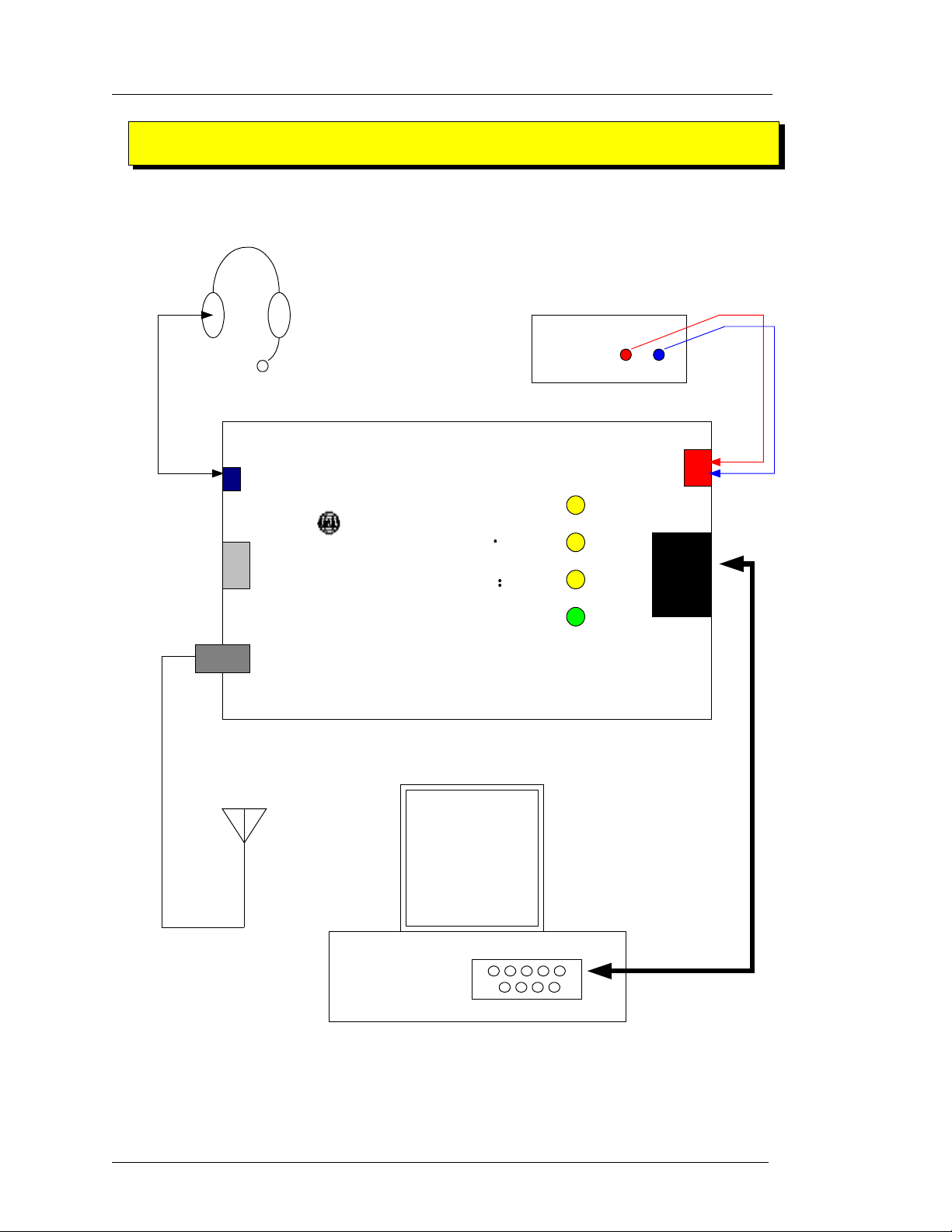
1.INSTALLATION METHOD
HeadSet
Power
Supply
(6~12V)
EAR/MIC
IDLEBUSYSMS PWR
UART2
Connector
AnyDATA
ANT
i PORT
+ -
Input
UART1
6~12V
ANT
8 Pin to 9 Pin
Cable
COM1
1) Supply the voltage of 6~12V to 2pin Connector of the EMII -1900.
2) Connect the UART1 to PC COM1 port with the RS-232C cable.
3)
Install the operating program.
EMII-1900 V1.0 AnyDATA.NET Proprietary Use Subject to Restrictions
Page 16
Interface Description EMII-1900 Service Manual Application Information
2. OPERATION METHOD
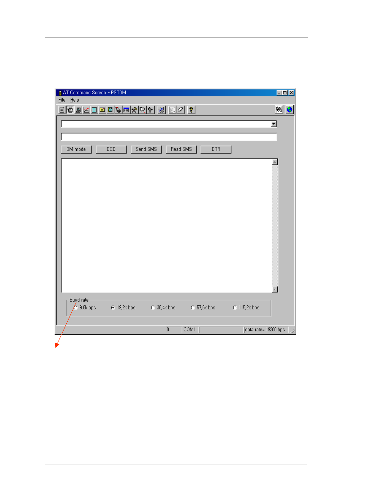
1) Run PSTDM program at Windows95 or Windows98
2) Set Buad rate to the modem… s.
3) Click [DM mode]
EMII-1900 V1.0 AnyDATA.NET Proprietary Use Subject to Restrictions
Page 17
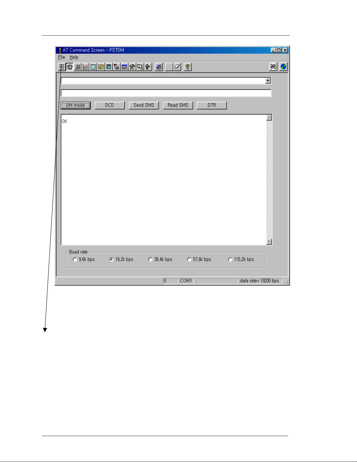
4) If OK is displayed in the message box, modem is now ready for
Interface Description EMII-1900 Service Manual Application Information
communication with PC.
5) Click MENU BAR icon.
EMII-1900 V1.0 AnyDATA.NET Proprietary Use Subject to Restrictions
Page 18
Interface Description EMII-1900 Service Manual Application Information
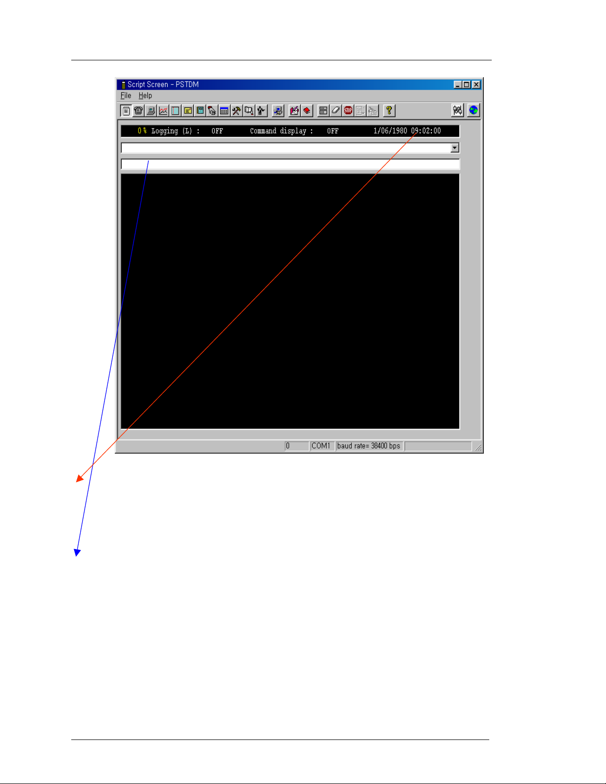
SCRIPTINPUT WINDOW
6) As shown in the picture above, service file input plane will be displayed
(See if clock is running. If it isn… t, communication with PC is not activated.
Repeat step 1 through 5, or reset the power of modem and repeat step 1 through 5)
7) Type NAM Programming script like the example shown below,
<NAM Programming script example>
Mode offline-d [ENTER]
nv_write name_nam {0," AnyDATA telecom "} [ENTER]
nv_write name_nam {1," AnyDATA telecom "} [ENTER]
Mode reset [ENTER]
EMII-1900 V1.0 AnyDATA.NET Proprietary Use Subject to Restrictions
Page 19

Interface Description EMII-1900 Service Manual Application Information
CHAPTER 3. Circuit Description
1. Overview
RFT3100 receives modulated digital signals from the MSM of the digital circuit and then, changes them into analog signals by
the digital/analog converter (DAC, D/A Converter) in order to create baseband signals. Created baseband signals are changed
into IF signals by RFT3100 and then, fed into the Mixer after going through AGC. IF signals that have been fed are mixed with
the signals of VCO and changed into the RF signals and then, they are amplified at the Power AMP. Finally, they are sent out
to the cell site via the antenna after going through the isolator and duplexer.
2. RF Transmit / Receive Part
2.1 CDMA Transmit End
8 bit I and Q transmit signals are inputted into 2 DACs (DIGITAL-TO-ANALOG CONVERTER) from
the output terminal I_DATA, I_DATA\, Q_DATA, Q_DATA\ of MSM through the input terminals
I_DATA, I_DATA\, Q_DATA, Q_DATA\ of RFT3100. Transmit signal input speed is two times of
TXCLK+, TXCLK- which are two transmit/receive reference frequency.
Among transmit signals being inputted, signals are inputted into I signal DAC when the transmit clock is
in the rise edge, whereas signals are inputted into Q Signal DAC during the drop edge. I and Q transmit
signals are compensated and outputted at MSM in order to compensate the 1/2 clock time difference
generated between reference clocks. In the signals coming out from the output terminal of DAC, there are
spurious frequency ingredients resulting from DAC output transition edge and parasite ingredients,
transmit clock frequencies and harmonics which are unwanted signals. Accordingly, spurious ingredients
are removed by passing the signals through LPF of passband 6.30KHz. Unlike the receive end, the
transmit end LPF requires no OFFSET adjustment. Analog baseband signals that have passed the CDMA
LPF are mixed with I and Q signals of frequency 130.38 MHz (260.76 MHz created in the RFT3100
internal VCO are divided by half into frequency 130.38MHz having the phase difference of 90 degrees) in
two mixers. The mixed signals are added again and converted into IF frequency 130.38 MHz ⥮630 KHz
(CDMA Spread Power Density Modulated Signals) and then, outputted.
2.2. Tx IF/Baseband Processors, RFT3100 (U102)
The RFT3100 includes digital-to-analog converters(DAC) for converting digital baseband to analog
baseband, low-pass filters, a mixer for up-converting to IF and an 85 dB dynamic range Tx AGC
amplifier. The RFT3100 has an IF mixer for upconverting analog baseband to IF, a programmable PLL
for generating Tx IF frequency, single sideband upconversion from IF to RF, two cellular and two PCS
driver amplifiers. The RFT3100 will operate over the follow Tx frequency ranges :
Cellular band 824MHz ~ 925MHz
PCS band 1750MHz ~1910MHz
EMII-1900 V1.0 AnyDATA.NET Proprietary Use Subject to Restrictions
Page 20

Interface Description EMII-1900 Service Manual Application Information
2.3. Transmit End Bandpass Filter (F102, F103)
Transmit signals that have been converted from IF signals into RF signals after passing through the
RFT3100(U102) are inputted into the Power Amp (U103) after passing once again through RF BPF
(F101) in order to filter out noise signals amplified during the amplification of RF signals after going
through RFT3100(U102). This is carried out in order to create power level inputted to the Power AMP via
RF BPF (F101). IL of a RF BPF is 2dB as a maximum, whereas the ripple in the passing band is
2dB(maximum). The degree of the suppression of transmit signals on receive band is at least 20dB or
greater. The maximum power that can be inputted is about 25dBm.
2.4. Power Amplifier (U102)
The power amplifier U102 that can be used in the CDMA and FM mode has linear amplification
capability, whereas in the FM mode, it has a high efficiency. For higher efficiency, it is made up of one
MMIC (Monolithic Microwave Integrated Circuit) for which RF input terminal and internal interface
circuit are integrated onto one IC after going through the AlGaAs/GaAs HBT (heterojunction bipolar
transistor) process. The module of power amplifier is made up of an output end interface circuit including
this MMIC. The maximum power that can be inputted through the input terminal is +17dBm and
conversion gain is about 28dB. RF transmit signals that have been amplified through the power amplifier
are sent to the duplexer and then, sent out to the cell site through the antenna in order to prevent any
damages on circuits, that may be generated by output signals reflected from the duplexer and re-inputted
to the power amplifier output end.
2.5. Description of Frequency Synthesizer Circuit
2.5.1 Voltage Control Temperature Compensation Crystal Oscillator(TXC201, VCTCXO)
The temperature range that can be compensated by TCX201 which is the reference frequency generator of
mobile terminal is -30 ~ +80 degrees. TCX201 receives frequency tuning signals called TRK_LO_ADJ
from MSM as 0.5V~2.5V DC via R and C filters in order to generate the reference frequency of
19.68MHz and input it into the frequency synthesizer of UHF band. Frequency stability depending on
temperature is ⥮ 2.0 ppm.
EMII-1900 V1.0 AnyDATA.NET Proprietary Use Subject to Restrictions
Page 21

Interface Description EMII-1900 Service Manual Application Information
2.5.2 UHF Band Frequency Synthesizer (U202)
Reference frequency that can be inputted to U202 is 3MHz~40MHz. It is the dual mode
frequency synthesizer (PLL) that can synthesize the frequencies of RF band 50MHz~1200MHz and IF
band 20MHz~300MHz. U202 that receives the reference frequency of 19.68MHz from TCX201 creates
30kHz comparison frequency with the use of internal program and then, changes the frequency of
1750MHz band inputted from U204 which is the voltage adjustment crystal oscillator into the comparison
frequency of 30kHz at the prescaler in U202. Then, two signal differences are calculated from the internal
phase comparator. The calculated difference is inputted to DC for adjusting the frequency of U174
through U172 No.2 PIN and external loop filter in order to generate UHF signals. In addition, outputs of
other PIN17 are inputted into BBA after going through the VRACTOR diode and tank circuit so that the
outputs of BBA internal receive end VCO are adjusted to 170.76MHz.
2.5.3 Voltage Control Crystal Oscillator (U204)
U204 that generates the LO frequency (1750MHz) of mobile terminal receives the output voltage of PLL
U202 and then, generates the frequency of 1720MHz at 0.7V and the frequency of 1780MHz at 2.7V. The
control voltage sensitivity is 23MHz/v and the output level is 1dBm(maximum). Since LO frequency
signal is very important for the sensitivity of mobile terminal, it must has good spurious characteristics.
U204 is -70dBc(maximum).
EMII-1900 V1.0 AnyDATA.NET Proprietary Use Subject to Restrictions
Page 22

Interface Description EMII-1900 Service Manual Application Information
3. Digital/Voice Processing Part
3.1 Overview
The digital/voice processing part processes the user's commands and processes all the digital and voice
signal processing in order to operate in the phone. The digital/voice processing part is made up of a
receptacle part, voice processing part, mobile station modem part, memory part, and power supply part.
3.2 Configuration
3.2.1 Voice Processing Part
The voice processing part is made up of an Integrated codec with microphone and earphone amplifiers,
two microphone inputs and one Auxiliary audio input, internal vocoder supporting 13kbps EVRC and
digital audio interface via USB. The anplifing voice signals out of MSM send to the earpiece or speaker
and signals coming out from MIC transfer to the audio processor
3.2.2 MSM (Mobile Station Modem) Part
MSM5105 is the core elements of CDMA terminal and carries out the functions of CPU, encoder,
interleaver, deinterleaver, Viterbi decoder, Mod/Demod, and vocoder.
3.2.3 Memory Part
The memory part is made up of a stacked MCP(Multi-Chip Package) Flash memory and SRAM cmos.
3.2.4 Power Supply Part
The power supply part is made up of circuits for generating various types of power, used for the
digital/voice processing part.
+4.0V from external DC(6~12V) is fed into six regulators(U601, U602, U603, U606, U607, U609). The
five regulators produces +3.0V for the Rx parts, Tx parts, Memory and MSM. The one regular produces
+2.7V ,VDD_A, VDD_C for the MSM.
EMII-1900 V1.0 AnyDATA.NET Proprietary Use Subject to Restrictions
Page 23
Interface Description EMII-1900 Service Manual Application Information
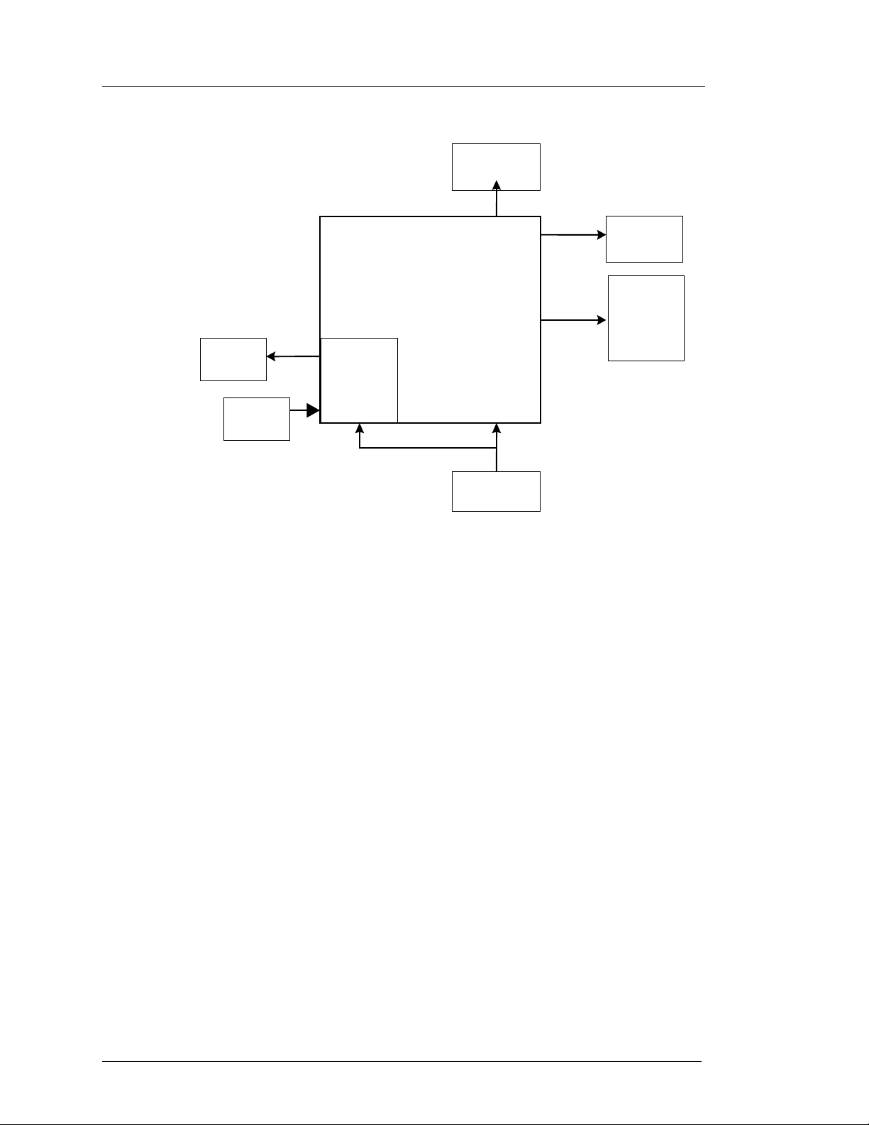
3.3 Circuit Description
MSM5105
Earpiece
AUDIO
Processor
Receptacle
Ringer
MCP(16M+
4M)
Mic
Power Supply
[Figure 3-1] Block Diagram of Digital/Voice Processing Part
3.3.1 MSM Part
MSM5105, which is U401, is the core element of CDMA system terminal that includes ARM7TDMI
microprocessor core. It is made up of a CPU, encoder, interleaver, deinterleaver, Viterbi decoder,
MOD/DEM, and vocoder. MSM5105, when operated in the CDMA mode, utilizes CHIPX8 (9.8304MHz)
as the reference clock that is received from IFR3000, and uses TCXO (19.68MHz) that is received from
TCX201. CPU controls the terminal operation. Digital voice data that have been inputted are
voice-encoded and variable-rated. Then, they are convolutionally encoded so that error detection and
correction are possible. Coded symbols are interleaved in order to cope with multi-path fading. Each data
channel is scrambled by the long code PN sequence of the user in order to ensure the confidentiality of
calls.
Moreover, binary quadrature codes are used based on Walsh functions in order to discern each channel.
Data created thus are 4-phase modulated by one pair of Pilot PN code and they are used to create I and Q
data.
When received, I and Q data are demodulated into symbols by the demodulator and then, de-interleaved
in reverse to the case of transmission. Then, the errors of data received from Viterbi decoder are detected
and corrected. They are voice decoded at the vocoder in order to output digital voice data.
EMII-1900 V1.0 AnyDATA.NET Proprietary Use Subject to Restrictions
Page 24

Interface Description EMII-1900 Service Manual Application Information
3.3.2 Memory Part
Memory part, MCP consists of 16M Flash memory and 4M static RAM.
In the MCP, there are programs used for terminal operation. The programs can be changed through down
loading after the assembling of terminals and data generated during the terminal operation are stored
temporarily and non-volatile data such as unique numbers (ESN) of terminals are stored.
3.3.3 Power Supply Part
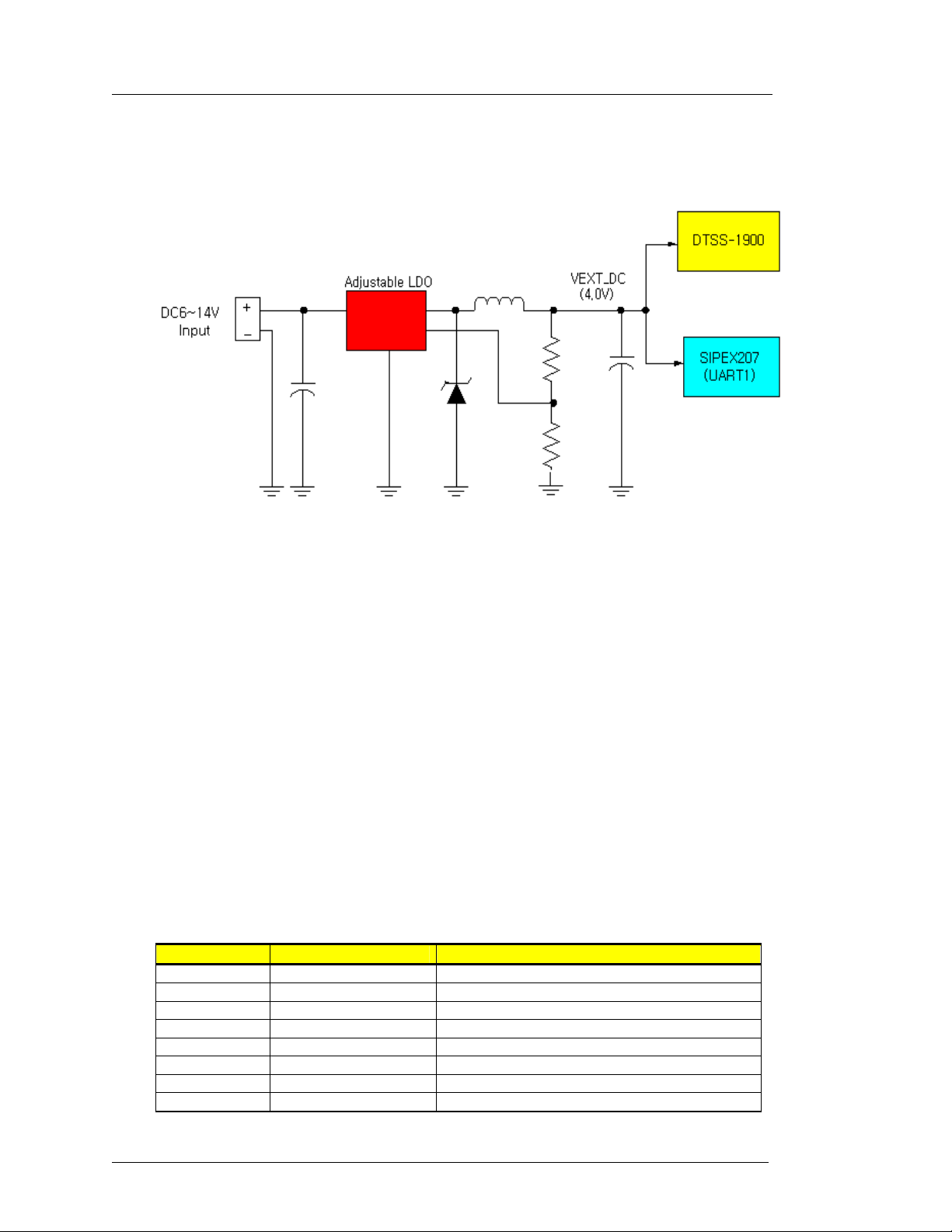
When the input voltage (4.0V) in the DTSS-1900 is fed to the five regulators generated +3.0V and the one
regular generated +2.7V. The generated voltages are used for MSM5105, RFT3100, IFR3000 and other
LOGIC parts. PWR ASIC is operated by the control signal SLEEP/ from MSM5105 and POWER_EN
signal.
3.3.4 Logic Part
The Logic part consists of internal CPU of MSM, MCP. The MSM5105 receives TCXO (=19.68Mz)
from VC-TCXO and CHIPX8 clock signals from the IFR3000, and then controls the module during the
CDMA and the FM mode. The major components are as follows:
CPU : ARM7TDMI core
MEMORY : MCP (MB84VD21182A-85-PBS : U505)
CPU
ARM7TDMI CMOS type 16-bit microprocessor is used and CPU controls all the circuitry. For the CPU
clock, 32.768KHz is used.
MCP(16M +4M)
MCP is used to store the terminal…s program. Using the down-loading program, the program can be
changed even after the terminal is fully assembled.
SRAM is used to store the internal flag information, call processing data, and timer data.
EMII-1900 V1.0 AnyDATA.NET Proprietary Use Subject to Restrictions
Page 25
Interface Description EMII-1900 Service Manual Application Information
4. Level Translator Part
4.1 EMII-1900 supply power to Modem(4.0V).
[Fig 4-1] The Block Diagram of Source (in brief)
4.2 UART Interface
The Universal Asynchronous Receiver Transmitter (UART) communicates with serial data that
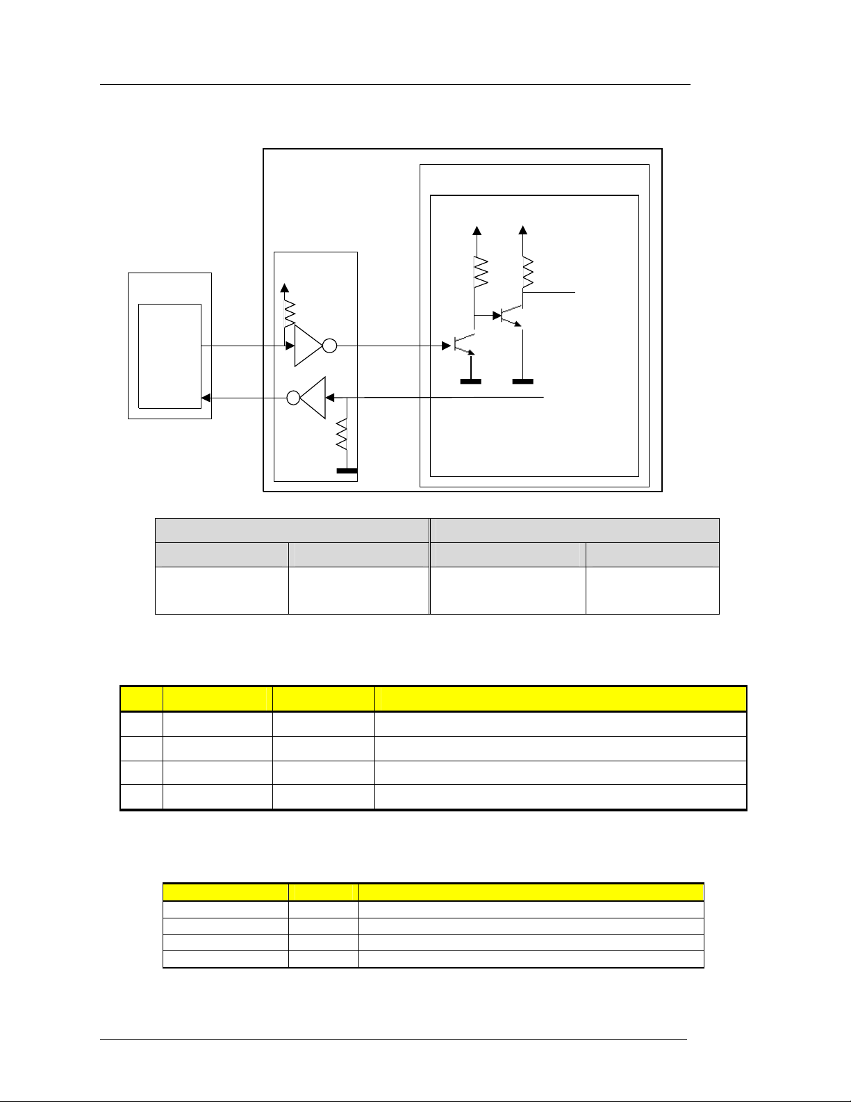
conforms the RS-232 Interface protocol. The modem provides 3.0V CMOS level outputs and 3.0V
CMOS switching input level. And all inputs have 5.0V tolerance but 3.0V or 3.3V CMOS logic
compatible signals are highly recommended.
All the control signals of the RS-232 signals are active low, but data signals of RXD, and TXD are
active high.
The UART has a 64byte transmit (TX) FIFO and a 64byte receive (RX) FIFO. The UART Features
hardware handshaking, programmable data sizes, programmable stop bits, and odd, even, no parity.
The UART operates at a 115.2kbps maximum bit rate.
4.2.1 UART Inter Pinouts
NAME DESCRIPTION CHARACTERISTIC
DP_DCD/ Data Carrier Detect Network connected from the modem
DP_RI/ Ring Indicator Output to host indicating coming call
DP_RTS/ Request to Send Ready for receive from host
DP_TXD Transmit Data Output data from the modem
DP_DTR/ Data Terminal Ready Host ready signal
DP_RXD Receive Data Input data to the modem
DP_CTS/ Clear to Send Modem output signal
GND Signal Ground Signal ground
EMII-1900 V1.0 AnyDATA.NET Proprietary Use Subject to Restrictions
Page 26
Interface Description EMII-1900 Service Manual Application Information
4.2.2 Signal level of RXD/TXD
PC
RS232
TX
RX
EMII-1900
SIPEX207
+4V
V
01 03
02 04
+3V +3V
DTS-800
MSM_output
MSM_input
Vout= 2.8V
RS232 PHONE
TX01 RX02 TX04 RX03
V
V
MAX
MIN
= 7.68V
= -7.68V
V
V
MAX
= -6.64V
MIN
= 6.50V
V
MAX
V
MIN
= 3.00V
= 0V
V
MAX
V
MIN
[Figure 4-2] Signal Level of RXD, TXD
4.3 LED State Indication
Name Enable Description
1 D1(IDLE) Low Stable State
2 D2(BUSY) Low State that Data transmit and receive between DTE and DCE
3 D3(SMS) Low Shot Message Service
4 D4(PWR) Low Power ON/OFF
4.4 The function of Real Audio Test( including Voice Test)
NAME TYPE DESCRIPSION
MIC+ I Microphone audio input
MIC- IS Ear/microphone set detect
EAR O Ear audio output
GND_A Audio ground
= 3.9V
= 0V
EMII-1900 V1.0 AnyDATA.NET Proprietary Use Subject to Restrictions
Page 27

Interface Description EMII-1900 Service Manual Application Information
CHAPTER 4. FCC Notice
This equipment has been tested and found to comply with the limits for a Class B digital device, pursuant to part 15
of the FCC Rules. These limits are designed to provide reasonable protection against harmful interference in a
residential installation. This equipment generates, uses and can radiate radio frequency energy and, if not installed
and used in accordance with the instructions, may cause harmful interference to radio communications. However,
there is no guarantee that interference will not occur in a particular installation. If this equipment does cause harmful
interference to radio or television reception, which can be determined by turning the equipment off and on, the user is
encouraged to try to correct the interference by one or more of the following measures:
Reorient or relocate the receiving antenna.
n
Increase the separation between the equipment and receiver.
n
Connect the equipment into an outlet on a circuit different from that to which the receiver is connected.
n
Consult the dealer or an experienced radio/TV technician for help.
n
EMII-1900 V1.0 AnyDATA.NET Proprietary Use Subject to Restrictions
Page 28

Interface Description EMII-1900 Service Manual Application Information
APPENDIX
1. Assembly and Disassembly Diagram
2. Block & Circuit Diagram
3. Part List
4. Component Layout
EMII-1900 V1.0 AnyDATA.NET Proprietary Use Subject to Restrictions
Page 29
Interface Description EMII-1900 Service Manual Application Information
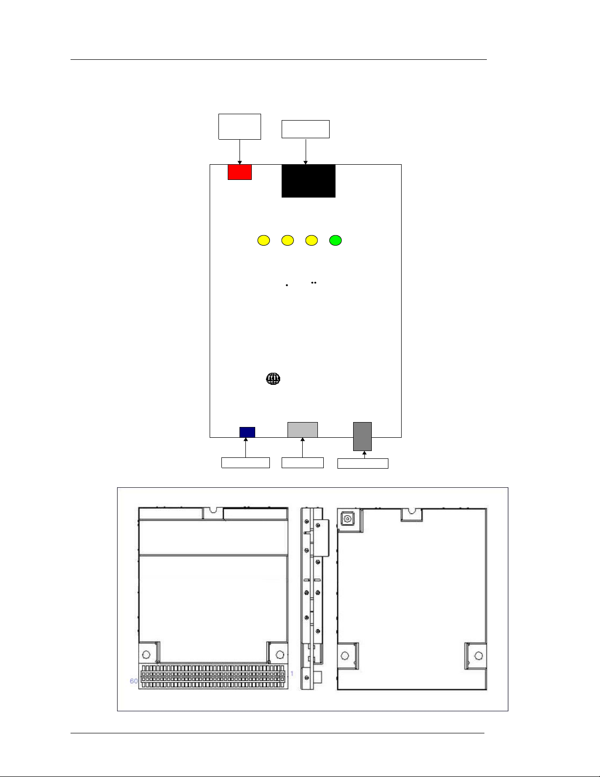
1. Assembly and Disassembly Diagram
DC6~12V
INPUT
RS232C
IDLE BUSY SMS PWR
i PORT
AnyDATA
EAR-MIC DEBUG
CDMA ANT
EMII-1900 V1.0 AnyDATA.NET Proprietary Use Subject to Restrictions
Page 30
Connector
Interface Description EMII-1900 Service Manual Application Information
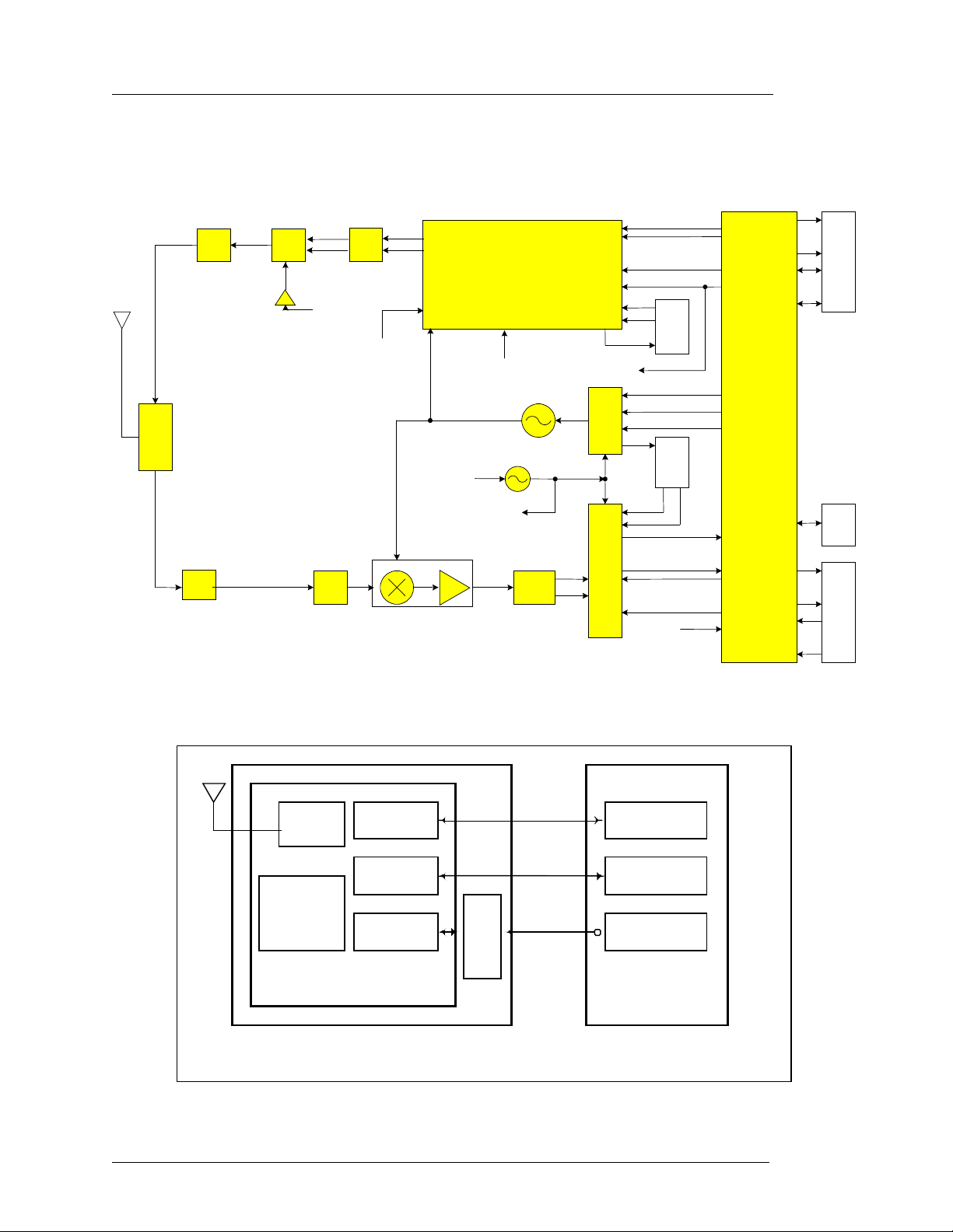
2. Block & Circuit Diagram
2.1. MODEM Block Diagram
DUPLEXER
PAM
SW437R
AB_SEL
RF Tx
SAW
TX_AGC_ADJ
TX Local
TRK_LO_ADJ
RFT3100
19.68MHz
19.68MHz
TCXO
VCO
TX_AGC_ADJ
PLL
Tx IF Tank
UHF_EN
PLL_DATA
PLL_CLK
MSM5105
Rx IF Tank
MCP
EAR &
MIC
LNA
RF Rx
SAW
2.2. EMII-1900 Block Diagram
ANT
RF Unit
MSM Inter.
CODEC
MSM5105
DTSS-1900
LDO(4V)
Down Mix
UART1
LDO(12V)
Rx IF SAW
IFR
3000
32.768KHz
RS-232
EARJACK
External PWR
(6~14V)
60 Pin
EMII-1900
Application Device
EMII-1900 V1.0 AnyDATA.NET Proprietary Use Subject to Restrictions
Page 31
Q102, Q302, Q303, Q304,
Interface Description EMII-1900 Service Manual Application Information
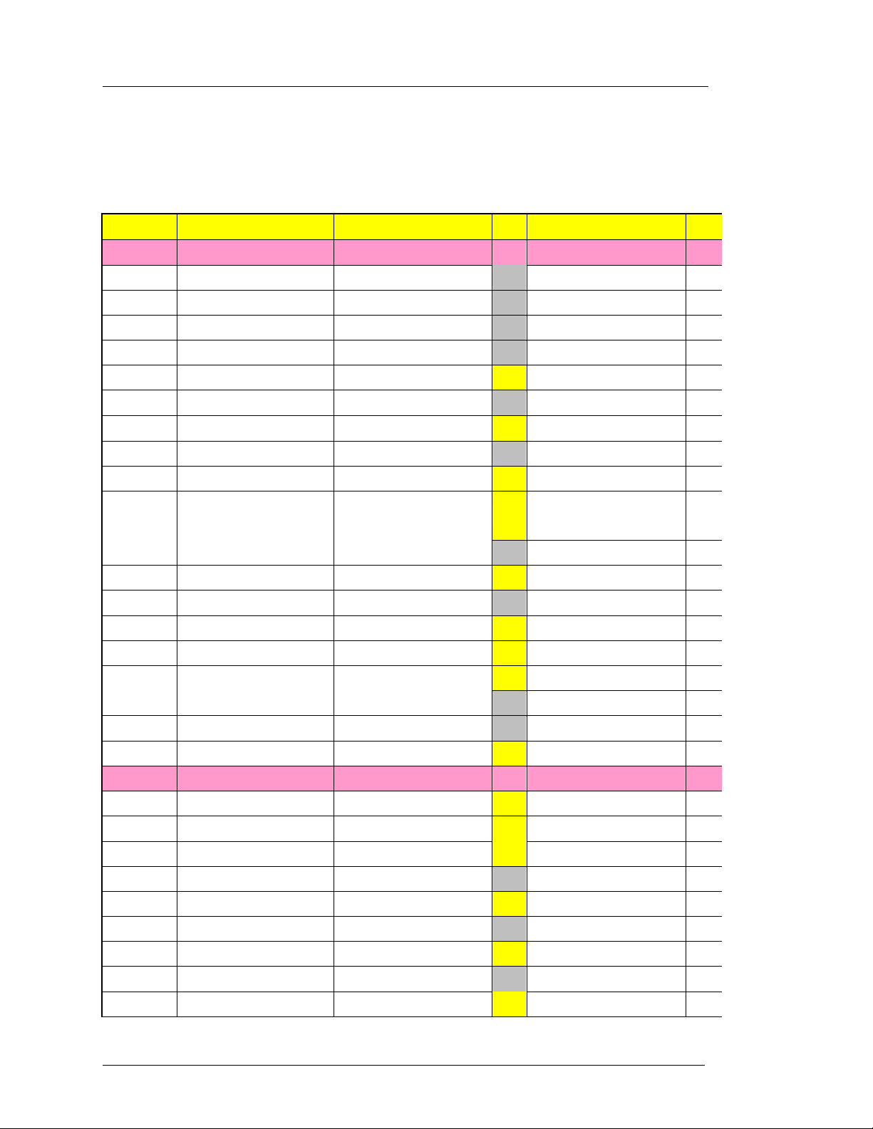
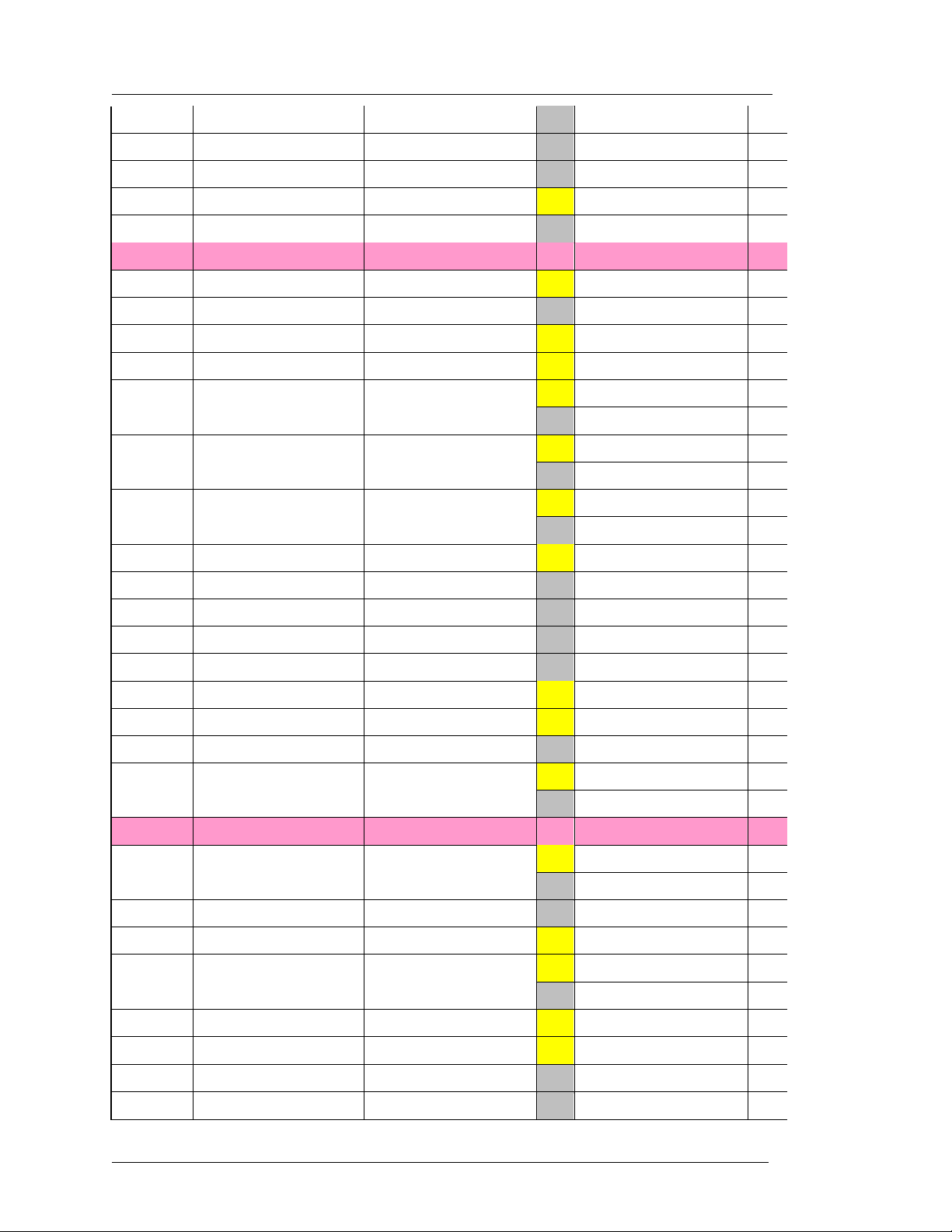
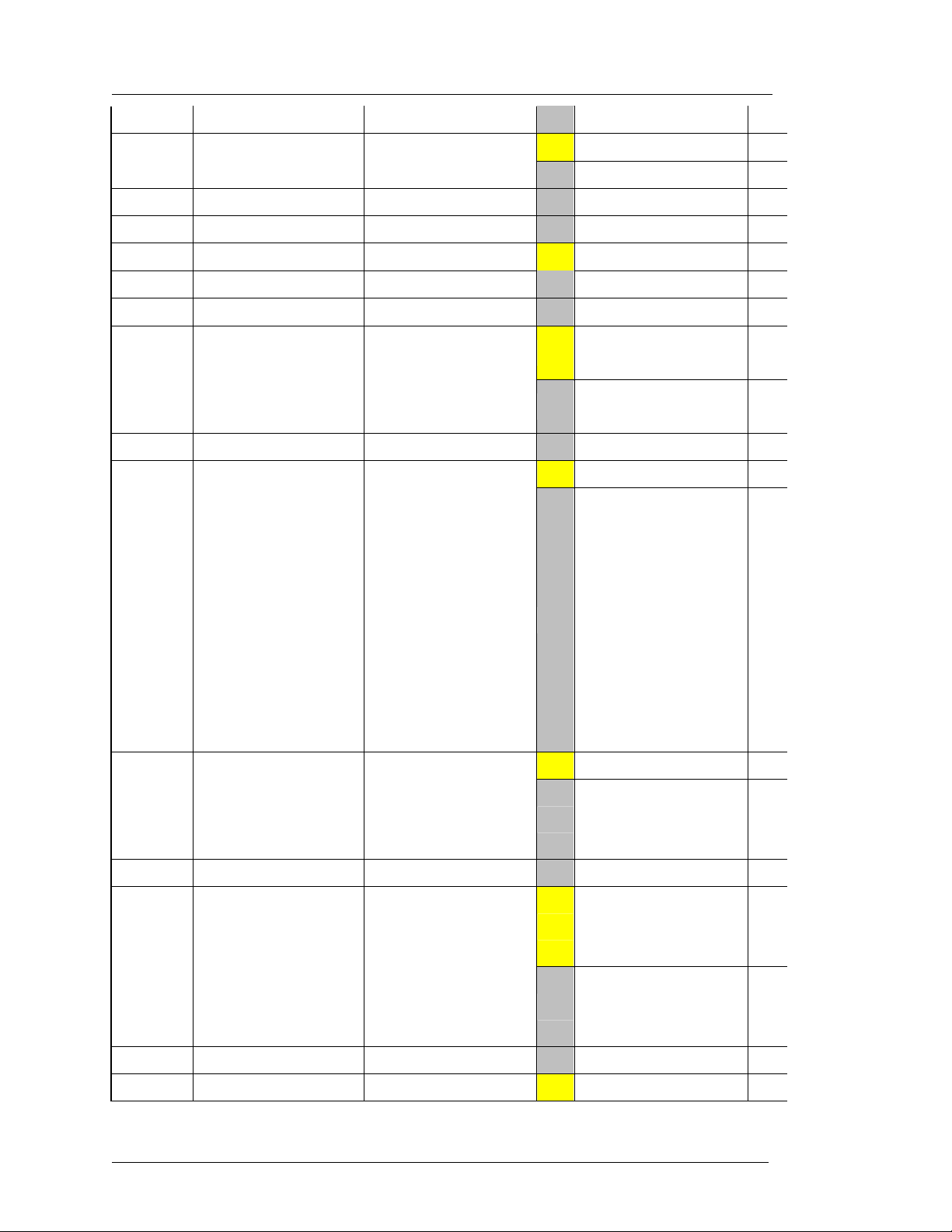
3. Part List
3-1 DTSS-1900 Partlist
NO COMPONENT NAME DESCRIPTION Lay.
LOGIC
1 MSM5105-A208FBGA-TR MSM5105 (208P) BOT U401 1
2 IFR3000-48BCCF-TR IFR3000 (48P) BOT U201 1
3 RFT31003-32BCCP-TR RFT3100 (32P) BOT U102 1
4 MB84VD21182A-85-PBS MCP(16M+4M) BOT U505 1
6 MIC5245-3.0VBM5 LDO (3.0V) TOP U601, U602, U603, U607, U609 5
7 MIC5245-2.7VBM5 LDO (2.7V) BOT U606, 1
8 TC7SHU04FU INVERTER TOP U205 1
9 FDC634P P CH-MOSFET(SSOT-6) BOT U104 1
10 S-80827ALNP-EDT-T2 RESET IC TOP U608 1
TOP
11 DTC124EE-TL DIGITAL TR
BOT Q104, 1
12 UMC4N-TR DIGITAL TR TOP Q306 1
13 UMH2N-TN DIGITAL TR BOT U504 1
14 UPS5819 SCHOTTKY DIODE TOP ZD601 1
DESIGN NUMBER Q'ty
Q305, Q307
6
15 B06B-4101-606 60PIN CONNECTOR TOP CON301 1
16 1SV281 VARACTOR DIODE
17 NT732ATD683K THERMISTOR BOT TH201 1
18 F0805B3R00FW FUSE (1608 Size) TOP FUSE1 1
RF
1 RI23110P PAM TOP U103 1
2 DFX1880J1960F DUPLEXER(US-PCS) TOP DUP101 1
3 B4934 RX IF SAW FILTER(5X5) TOP FL103 1
4 B4135 RX RF SAW FILTER(3X3) BOT FL102 1
5 LJ49A TX RF SAW FILTER(3X3) TOP FL101 1
6 VC_3R0A80_1750A VCO BOT U204 1
7 CMY212 DOWN MIXER TOP U101 1
8 LMX2354SLBX PLL BOT U202 1
9 KT16-DCV30L-19.68M VC-TCXO TOP TCX201 1
TOP VD201, VD202 2
BOT VD101, VD102 2
EMII-1900 V1.0 AnyDATA.NET Proprietary Use Subject to Restrictions
Page 32
Interface Description EMII-1900 Service Manual Application Information
10 SSP-T6 X-TAL(32.768K-7.0PF) BOT X401 1
11 BFP620 LNA BOT Q101 1
12 BFP420 BUFFER AMP BOT Q201 1
13 SW437 SW-437 TOP SW102 1
14 MCA-ST-00T MOBLE SWITHCH BOT SW101 1
INDUCTOR
1 0603CS-22NXG-BC CHIP COIL(2%) TOP L203 1
2 0603CS-27NXG-BC CHIP COIL(2%) BOT L113 1
3 0603CS-39NXG-BC CHIP COIL(2%) TOP L106 1
4 0603CS-56NXG-BC CHIP COIL(2%) TOP L105 1
5 CI-B1005-27NSJT IND/2.7N(+-0.3nH)
6 CI-B1005-33NSJT IND/3.3N(+-0.3nH)
8 CI-B1005-47NSJT IND/4.7N(+-0.3nH)
9 CI-B1005-56NSJT IND/5.6N (+-5%) TOP L116 2
10 CI-B1005-101NSJT IND/100N (+-5%) BOT L115 2
11 CI-B1608-150NJJT IND/15N (+-5%) BOT L101 1
12 CI-B1608-4R7NJJT IND/4.7N (+-5%) BOT L103 1
13 CI-B1608-330NJJT IND/33N (+-5%) BOT L104 1
14 CI-B1608-560NJJT IND/56N (+-5%) TOP L114 1
15 CI-B1608-680NJJT IND/68N (+-5%) TOP L121 1
16 CI-B1608-270NJJT IND/27N (+-5%) BOT L117, L118 2
17 BLM1608A601SPT FERITE BEAD
CAPACITOR
TOP L100 1
BOT L111, L112 2
TOP L120 1
BOT L110 1
TOP L119 1
BOT L201 1
TOP BL102, BL605, BL607 3
BOT BL202, BL606 2
1 GRM36COG0R5C50PT 0.5pF-1005 Cap
2 GRM36C0G1R0C50PT 1pF-1005 Cap BOT C173 1
2 GRM36C0G1R5C50PT 1.5pF-1005 Cap TOP C113 1
3 GRM36C0G2R0C50PT 2pF-1005 Cao
5 GRM36COG040D50PT 4pF-1005 Cap TOP C133 4
6 GRM36COG0800D50PT 8pF-1005 Cap TOP C129 1
7 GRM36COG100080J50PT 10pF-1005 Cap BOT C107, C112, C147, C410 4
8 GRM36COG150J50PT 15pF-1005 Cap BOT C158, C402, C403 3
TOP C169, C186 1
BOT C102 1
TOP C135, C145, C212 1
BOT C249 1
EMII-1900 V1.0 AnyDATA.NET Proprietary Use Subject to Restrictions
Page 33
C114, C122, C132, C417, C418,
C139, C142, C185, C280,
C131, C301, C302, C303, C304,
C305, C307, C308, C312, C313,
C314, C315, C316, C317, C318,
C319, C320, C321, C322, C323,
C324, C325, C326, C327, C328,
C329, C330, C331, C332, C333,
C334, C335, C336, C337, C338,
C339, C340, C341, C342, C343,
344, C345, C346, C347, C348,
C136, C137, C138, C141, C143,
C144, C166, C191, C219,
C110, C115, C128, C209, C258,
C453, C455, C603, C611, C618,
C205, C206, C215, C216, C220,
C221, C240, C250, C283, C290,
Interface Description EMII-1900 Service Manual Application Information
9 GRM36C0G180J50PT 18pF-1005 Cap BOT C130 1
10 GRM36COG220J50PT 22pF-1005 Cap
TOP C211, C213 2
BOT 1
11 GRM36COG240J50PT 24pF-1005 Cap BOT C164, C165 2
12 GRM36COG270J50PT 27pF-1005 Cap BOT C246 1
13 GRM36C0G390J50PT 39PF-1005 Cap TOP C123, C126 2
14 GRM36C0G470J50PT 47pF-1005 Cap BOT C152, C230, C231, C232,
15 GRM36C0G820J50PT 82pF-1005 Cap BOT C146, C151, 2
TOP
C501
16 GRM36COG101J50PT 100pF-1005 Cap
BOT
C285, C288
17 GRM36COG221J50PT 220pF-1005 Cap BOT C155, C156 2
TOP C127, C306, C309, C310, C311 5
6
5
19 GRM36COG471J50PT 470pF-1005 Cap
20 GRM36X7R102K50PT 1nF-1005 Cap
21 GRM36COG472J50PT 4.7nF-1005 Cap BOT C111, 1
22 GRM36COG103J50PT 10nF-1005 Cap
BOT
C
C349, C350
TOP C118, C120, C121, C451 4
BOT
C243, C284, C289, C470
TOP
C620, C622, C630, C641
BOT
C450, C460, C614
47
13
14
13
23 GRM36COG123J50PT 12nF-1005 Cap BOT C425, C427 2
24 GRM36Y5V223Z25PT 22nF-1005 Cap TOP C421 1
EMII-1900 V1.0 AnyDATA.NET Proprietary Use Subject to Restrictions
Page 34
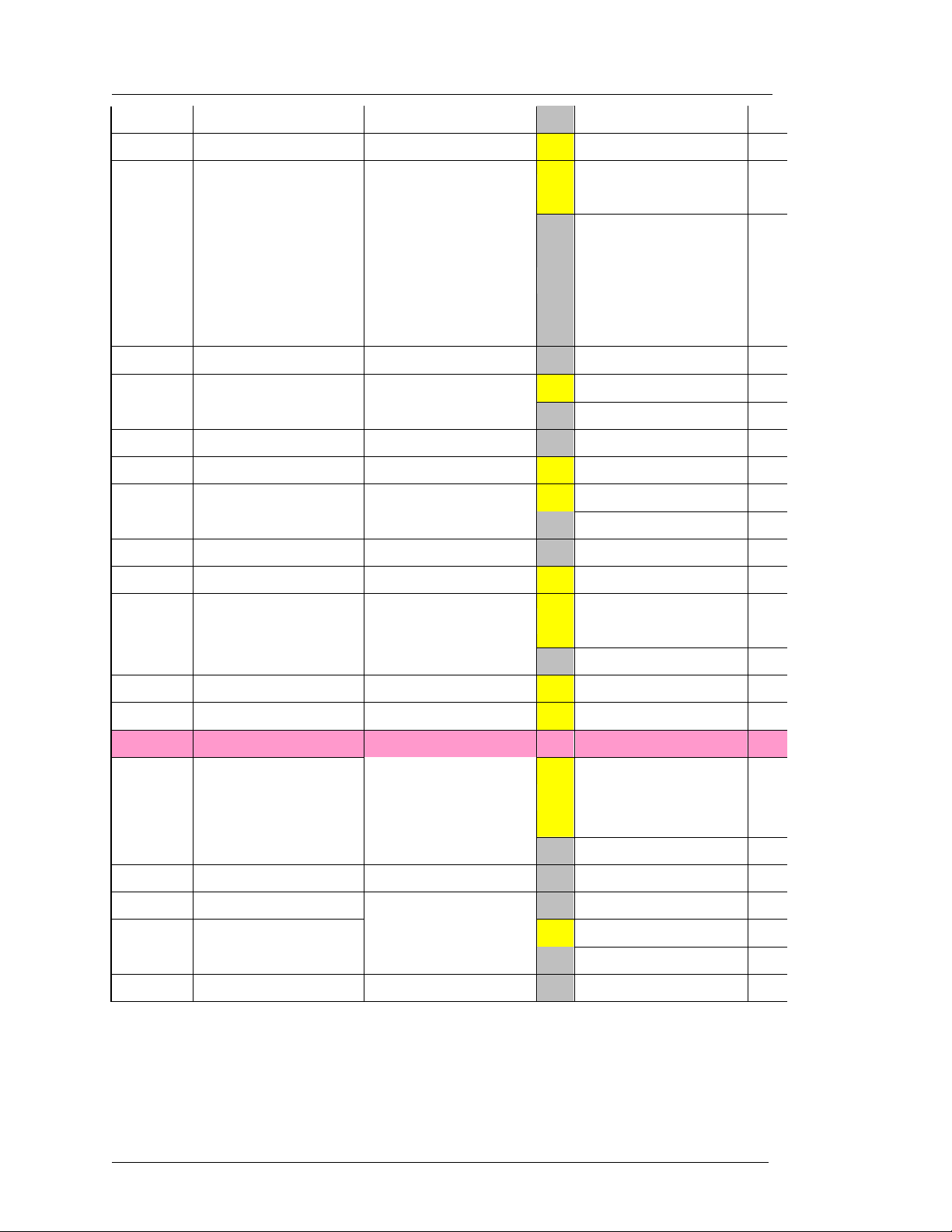
C170, C259, C270, C435, C452,
GRM36Y5V104Z25PT
C159, C160, C218, C222, C223,
8, C229, C235,
C260, C265, C286, C287, C291,
C423, C424, C426, C428, C701,
C124, C140, C604, C608, C612,
R143, R100, R156, R221,
R250, R611, R702, VA601,
Interface Description EMII-1900 Service Manual Application Information
BOT C420 1
25 GRM36Y5V683Z25PT 68nF-1005 Cap TOP C150 1
TOP
C454, C514, C623
26
27 GRM36COG105J50PT 1uF-1005 Cap BOT C101, C108, C109, 3
28 GRM39COG102J50PT 1nF-1608 Cap
29 GRM39Y5V103Z25PT 10nF-1608 Cap BOT C281 1
30 GRM39Y5V104Z25PT 100nF-1608 Cap TOP C207 1
31 GRM39Y5V224Z25PT 220nF-1608 Cap
32 GRM39Y5V684Z25PT 680nF-1608 Cap BOT C149 1
33 TA-6R3TCMS100M-PR Tan Cap (10uF/6.3V/P) TOP C269, C422, C625 3
34 TA-6R3TCMS4R7M-PR Tan Cap (4.7uF/6.3V/P)
100nF-1005 Cap
C226, C22
BOT
C702
TOP C253 1
BOT C148 1
TOP C214 1
BOT C282 1
TOP
C619, C621
23
8
7
BOT C616 1
35 TA-010TCR330K-A Tan Cap (33uF/6.3V/A) TOP C419 1
36 TA-010TCR101K-A Tan Cap(100uF/6.3V/A) TOP C125, C626 2
RESISTOR
1 MCR01MZSJX000 0W 5%-1005 Resistor
2 MCR01MZSJX100 10W 5%-1608 Resistor BOT L102 1
2 MCR01MZSJX100 10W 5%-1005 Resistor BOT R103, R244 2
3 MCR01MZSJX101 100W 5%-1005 Resistor
4 MCR01MZSJX331 330W 5%-1005 Resistor BOT R231, R240, R402 3
TOP
C134
BOT R140, R180, R206, R290, 5
TOP R130, R280 2
BOT R105, R243, R246 5
6
EMII-1900 V1.0 AnyDATA.NET Proprietary Use Subject to Restrictions
Page 35
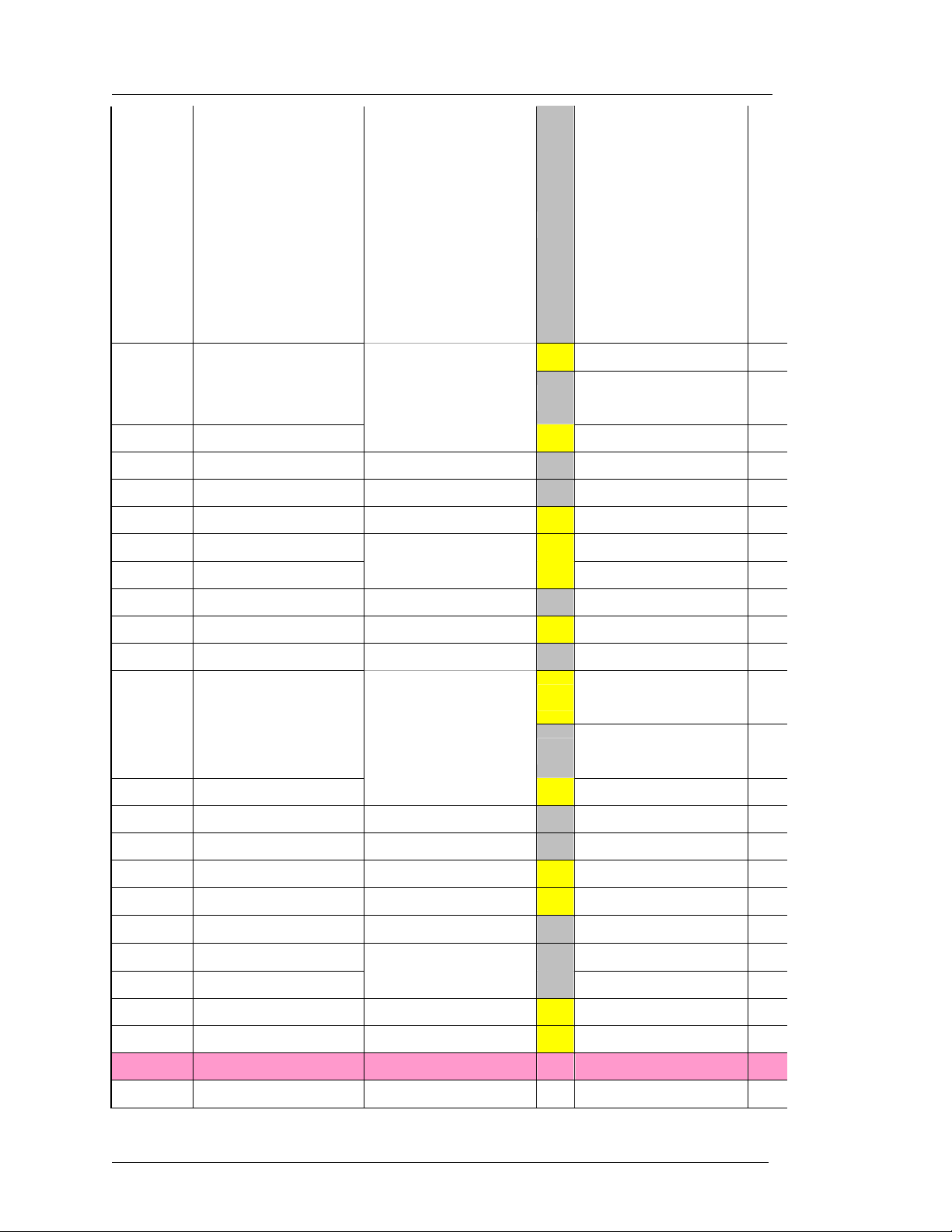
R301, R302, R303, R308, R309,
R317, R318, R319, R320, R321,
, R325, R326,
R327, R328, R329, R340, R341,
R342, R343, R344, R345, R346,
R347, R348, R349, R350, R351,
R352, R353, R354, R355, R356,
R357, R358, R359, R360, R361,
45
R104, R220, R223, R224, R241,
R111, R305, R307, R311, R312,
R102, R114, R116, R207, R208,
Interface Description EMII-1900 Service Manual Application Information
R322, R323, R324
5 MCR01MZSJX471 470W 5%-1005 Resistor BOT
R362, R363, R364, R365, R366
TOP R210, R455, R610 3
6 MCR01MZSJX102 1KW 5%-1005 Resistor
BOT
R410
7 MCR01MZSJX152 1.5KW 5%-1005 Resistor TOP R421 1
8 MCR01MZSJX182 1.8KW 5%-1005 Resistor BOT R115 1
9 MCR01MZSTX202 2KW 5%-1005 Resistor BOT R203 1
6
10 MCR01MZSTX222 2.2KW 5%-1005 Resistor TOP R200, R420 2
11 MCR01MZSJX332 3.3KW 5%-1005 Resistor TOP R202 1
12 MCR01MZSJX472 4.7KW 5%-1005 Resistor TOP R470 1
13 MCR01MZSJX512 5.1KW 5%-1005 Resistor BOT R201 1
14 MCR01MZSJX682 6.8KW 5%-1005 Resistor TOP R204, R205 2
15 MCR01MZSJX822 8.2KW 5%-1005 Resistor BOT R209 1
TOP
R314, R316, R475, R701
16 MCR01MZSJX103 10KW 5%-1005 Resistor
BOT
R424, R425, R501, R502
17 MCR01MZSJX223 22KW 5%-1005 Resistor TOP R310, R315, R313, R330 4
18 MCR01MZSJX273 27KW 5%-1005 Resistor BOT R101 1
19 MCR01MZSJX363 36KW 5%-1005 Resistor BOT R211 1
20 MCR01MZSJX104 100KW 5%-1005 Resistor TOP R189, R253, R260 3
21 MCR01MZSJX154 150KW 5%-1005 Resistor TOP R263 1
22 MCR01MZSJX184 180KW 5%-1005 Resistor BOT R422, R423 2
23 MCR01MZSJX504 500KW 5%-1005 Resistor BOT R427 1
9
9
24 MCR01MZSFX1212 12.1KW 1%-1005 Resistor BOT R119 1
25 MCR01MZSFX1003 100KW 1%-1005 Resistor TOP R222 1
26 MCR01MZSFX1004 1MW 1%-1005 Resistor TOP R117, R118 2
타
1 DTSS-1800 V0.3 PCB Main PCB 1
EMII-1900 V1.0 AnyDATA.NET Proprietary Use Subject to Restrictions
Page 36
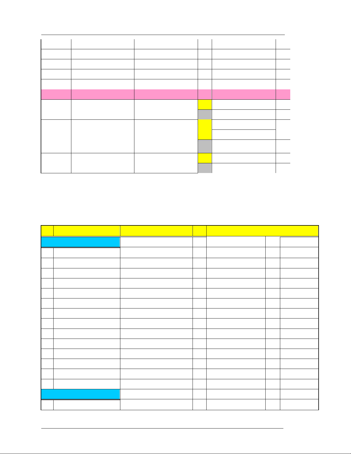
8
Interface Description EMII-1900 Service Manual Application Information
2 DTSS-1800 TOP COVER TOP COVER 1
3 DTSS-1800 TOP FRAME TOP FRAME 1
4 DTSS-1800 BOT COVER BOT COVER
5 DTSS-1800 BOT FRAME BOT FRAME 1
6 DTSS-1800 LABEL LABEL 1
DNI
1 RESISTOR
2 CAPACITOR
3
타
1
TOP R150, R107, R142, R254, R370 4
BOT R106, R155 2
C168
TOP
BOT C187, C224, C352 4
TOP VA301, L130 1
BOT
3-2. EM Main Board Partlist
1
28. Jan. 2002
No
LOGIC
Commponent Name
Description
1 SMA R/A(F)+ MCA Cable SMA(F) + MCA
2 PH127-60SMD-16H-2.0 60pin connetor
3 TC7SHU04F inverter
4 UMT2907A PNP TR
5 SP207-EA Tranceiver IC
6 MIC4576BU LDO (TO-263)
7 MBRS360T3 Schottky Diode
657PL8 8pin Modular Housing
9 BL-2141N LED(Green)
10 BL-3141N LED(Yellow)
11 HSJ1621-019011 EARJACK
12 53047-0310 1.25mm male 3pin
13 5268 2.5mm male 3pin°
14 5268 2.5mm male 2pin°
RESISTOR
Lay
TOP
BOT
TOP
TOP
TOP
TOP
TOP
TOP
TOP
TOP
TOP
TOP
TOP
TOP
DESIGN NO Vendor
1
CDMA 1 LINK Tec.
CN1 1 SKY Elec.
U19 3 TOSHIBA
U14,16,17 1 ROHM
U2 1 SIPEX
U3 1 MICREL
ZD1 1 MOTOROLA
J2 1 ARIN
D4 1 BRT
D1,D2,D3 3 BRT
U15 1 HOSIDEN
CN10 1 MOLEX
CN2 1 MOLEX
J1 1 MOLEX
15 MCR03MZSJX000 RESISTOR(1608) 0R
EMII-1900 V1.0 AnyDATA.NET Proprietary Use Subject to Restrictions
R30,R31,R44,R45, 6 ROHM
TOP
Page 37
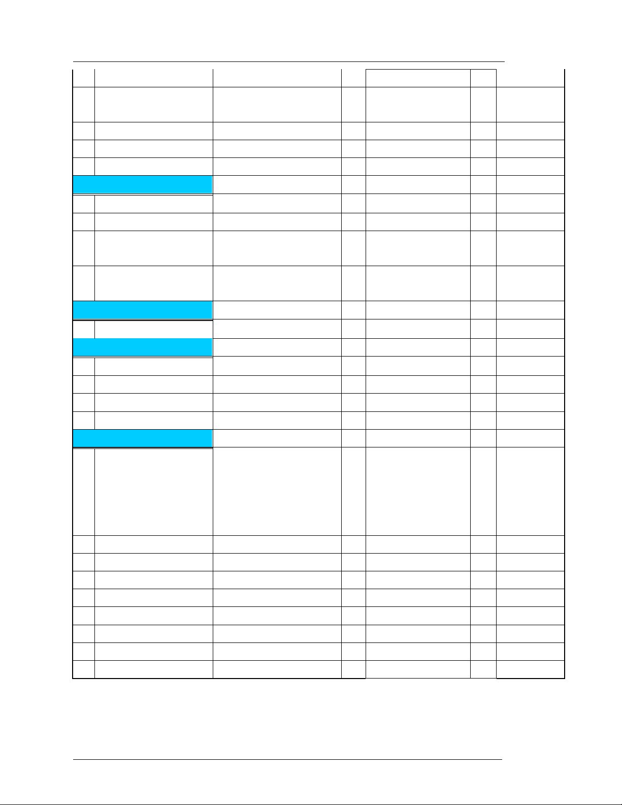
23
Interface Description EMII-1900 Service Manual Application Information
R46,R47
16 MCR03MZSJX101 RESISTOR(1608) 100R
17 MCR03MZSJX332 RESISTOR(1608) 3.3K
18 MCR03MZSJX472 RESISTOR(1608) 4.7K
19 MCR03MZSJX103 RESISTOR(1608) 10K
CAPACITOR
20 GR39COG471J50PT 470pF -1608 -capacitor
21 TA-035TCMR10M-AR TANTAL 0.1uF/35V
470uF/16V(10x10.5)
22
Elec. Cap (chip type)
"MVK" 85ɐC
1000uF/6.3V(10x10.5)
Elec. Cap (chip type)
"RGV"85ɐC
INDUCTOR
24 PL52C-33-1000 COIL INDUCTOR (33uH)
The Others
25 EM(II)_PCB _V0.1 EM(II)_PCB_MAIN_ V0.1
26 EM-BODY-00 BODY
R7,R8,R9,R34,R35,
TOP
7
R36,R37
R1,R2,R3 3 ROHM
TOP
R6 3 ROHM
TOP
R5 3 ROHM
TOP
C9 1 MURATA
TOP
C5,C6,C7,C8 3 TOWA
TOP
C1 1 SAMYANG
TOP
C2 1 RUBYCON
TOP
L2 1 COOPER
TOP
UNIC Elec.
TOSUNG
ROHM
27 EM-FRONT-00 FRONT
28 EM-REAR-00 REAR
DNI
29 DNI RESISTOR
30 DNI CAPACITOR
31 DNI DA114
32 DNI INDUCTOR
33 DNI MIC5205-3.0V
34 DNI TC74HC07AF(SOP-14)
35 DNI TC74HC4052AFT(SOP-16)
36 DNI 53047-0810(8PIN)
37 DNI 5268(3PIN)
TOSUNG
TOSUNG
R4,R13,R14,R15,
R16, R17,R18,R19,
R20,R21,R22,R23,
TOP
20
R24,R25,R26,R27,
R40,R41,R42,R43
C3,C4 2
TOP
D5 1
TOP
L1 1
TOP
U4 1
TOP
U6 1
TOP
U5 1
TOP
U7 1
TOP
CN3, CN4 2
TOP
EMII-1900 V1.0 AnyDATA.NET Proprietary Use Subject to Restrictions
Page 38

Interface Description EMII-1900 Service Manual Application Information
4. Component Layout
EMII-1900 V1.0 AnyDATA.NET Proprietary Use Subject to Restrictions
 Loading...