

Page 1

CDMA DATA TERMINAL
DTEV-Dual Reference Manual
Application Information
AnyDATA.NET
International Contact
AnyDATA Corp.
18902 Bardeen Ave
Irvine, CA 92612-1522, U.S.A.
e-mail : [email protected]
November, 21, 2005
DTEV-Dual
AnyTime AnyPlace Any Wireless Data Solutions™
Korea Contact
AnyDATA.NET
Hanvit Bank Bldg. 6th Fl., 1-12
Byulyang-dong Kwachon,
Kyunggi-do, Korea
e-mail : [email protected]
Page 2

AnyDATA.NET Inc. AnyTime AnyPlace Any Wireless Data Solution
TM
Notice
All data and information contained in or disclosed by this document are confidential and proprietary
information of AnyDATA.NET Inc., and all rights therein are expressly reserved. By accepting this
material, the recipient agrees that this material and the information contained therein are held in
confidence and in trust and will not be used, copied, reproduced, or distributed in whole or in part, nor its
contents revealed in any manner to others without the express written permission of AnyDATA.NET Inc.
AnyDATA.NET Inc. does not assume any liability arising out of the application or use of its products.
AnyDATA.NET Inc. assumes no responsibility for any damage or loss resulting from the misuse of its
products. AnyDATA.NET Inc. assumes no responsibility for any loss or claims by third parties, which
may arise through the use of its products. AnyDATA.NET Inc. assumes no responsibility for any damage
or loss caused by the deletion or loss of data as a result of malfunctions or repairs.
The information contained in this document is subject to change without notice. Information contained
herein is for reference only and does not constitute a commitment on the part of AnyDATA.NET Inc.
Although the information in this document has been carefully reviewed and it’s believed to be reliable,
AnyDATA.NET Inc. assumes no responsibility or liability for any errors or inaccuracies that may appear
in this document nor are they in anyway responsible for any loss or damage resulting from the use (or
misuse) of this document.
It is advised for the customers to contact our engineers for more information with respect to Keypad, audio
interface, RF interface and input power supply before they start an actual design.
OEM integrators and installers are instructed that the phrase 'This device contains transmitter FCC ID:
P4M-DTEVDUAL must be placed on the outside of the host.
Warning: Exposure to Radio Frequency Radiation
!
The radiated output power of this device is far below the FCC radio frequency exposure limits.
Nevertheless, the device should be used in such a manner that the potential for human contact
during normal operation is minimized. In order to avoid the possibility of exceeding the FCC
radio frequency exposure limits, human proximity to the antenna should not be less than 20cm
during normal operation and the gain of the antenna must not exceed 1dBi
All Rights Reserved.
AD-2001-06-28 Ver 1.1
-2-
Page 3

AnyDATA.NET Inc. AnyTime AnyPlace Any Wireless Data Solution
Contents
1 Introduction
1.1 Purpose
1.1.1 Features
1.1.2 Applications
1.2 Organization
1.3 Revision History
1.4 Reference
1.5 Acronym List
2 Overview
2.1 Application Description
TM
2.2 Technical Specifications
2.2.1 General Specification
2.2.2 Receive Specification
2.2.3 Transmit Specification
2.2.4 gpsOne Receiver Specification
2.2.5 Standards
2.3 Interface Diagram
3 PIN Description
3.1 I/O Description Parameters
3.2 PIN Names and Pin-outs
3.2.1 100-PIN Connector
3.2.2 100-PIN Connector Pin-out (Top view)
4 Interface Descriptions
4.1 Overview
4.2 Powering Up the Module
4.2.1 External Supply
All Rights Reserved.
AD-2001-06-28 Ver 1.1
-3-
Page 4

AnyDATA.NET Inc. AnyTime AnyPlace Any Wireless Data Solution
4.2.2 Keypad Power On and Supply Input to BATT_INT
4.3 Power Down Registration Protocol for CDMA device
4.3.1 Using AT command ( When Vcc is applied to VEXT_DC
4.3.2 Using POWER_ON ( Only when Vcc is applied to VBATT_INT )
4.4 Stereo Wideband CODEC Interface
4.4.1 Microphone and Earphone Interface
4.4.2 Stereo Headphone Interface
4.4.3 Digital PCM Interface
4.4.4 Stereo DAC Interface
4.5 UART Interface
TM
4.5.1 UART1 Interface
4.5.2 UART2 R-UIM Interface
4.5.3 UART3 Debug Port Interface
4.5.4 USB Interface
4.6 General Purpose Interface
4.7 User Interface
4.7.1 Key Pad
4.7.2 MultiMediaCard Controller
4.7.3 Vibration Motor Driver
4.7.4 LED Interface
4.8 External Bus Interface II (or LCD interface )
4.9 RF Interface
4.9.1 Antenna for Primary RF Chain
4.9.2 Antenna for Secondary RF Chain
All Rights Reserved.
AD-2001-06-28 Ver 1.1
-4-
Page 5

AnyDATA.NET Inc. AnyTime AnyPlace Any Wireless Data Solution
5 Electrical Specifications
5.1 DC Electrical Specifications
5.1.1 Absolute Maximum Ratings
5.1.2 Recommended Operating Conditions
5.1.3 Power Consumption
5.1.4 Serial Interface Electrical Specifications
5.1.5 Multi-Purpose Pin Specifications
5.1.5.1 Multi-Purpose Pin Configured
5.1.5.2 Multi-Purpose Pin Configured as a Bidirectional I/O
5.1.5.3 Multi-Purpose Pin Configured as an Analog
6 Mechanical Dimensions
6.1 DTEV-1000 Outline
TM
6.2 100-Pin Connector Mechanical Dimension
6.3 RF Connector
6.3.1 Cable Assembly, Sunridge Corp Part
6.3.1.1 Bulkhead SMA Type cable : MCB2G-RH-59-LLL-SMAJB101
6.3.1.2 PCB mountable right angle SMA cable : MCB2G-RH-59-LLL-SMAJX103
6.3.1.3 Contact Info.
6.3.2 Murata Part
7 Application Schematic
8 Module Picture
All Rights Reserved.
AD-2001-06-28 Ver 1.1
-5-
Page 6

AnyDATA.NET Inc. AnyTime AnyPlace Any Wireless Data Solution
Figures
Figure 2-1 Interface Block Diagram ………………………………………………………....17
Figure 3-1 100-PIN Connector Pinouts ...................................................................................22
Figure 4-7.1 Keypad Matrix ....................................................................................................32
Figure 4-7.2 MMC Bus Circuitry Diagram .............................................................................34
Figure 6-1 DTEV-Dual Outline …............................................................................................. 41
Figure 6-2 100-pin Connector ….................................................................................................42
Figure 6-3.1.1 Bulkhead SMA Type cable …..............................................................................43
Figure 6-3.1.2 PCB mountable right angle SMA cable…….…………………………….......43
Figure 7 Application Schematic................................................................................................. 45
Figure 8 Module Picture..............................................................................................................46
TM
All Rights Reserved.
AD-2001-06-28 Ver 1.1
-6-
Page 7

AnyDATA.NET Inc. AnyTime AnyPlace Any Wireless Data Solution
Tabl es
Table 1-1 Revision History............................................................................................................9
Table 1-2 Acronym List...............................................................................................................10
Table 2-1 General Specifications..................................................................................................13
Table 2-2 Receiver specifications…………………………………………................................14
Table 2-3 Transmitter Specifications...........................................................................................15
Table 2-4 gpsOne Receiver Specifications……………………………………………………..15
Table 3-1 I/O Description Parameters.........................................................................................18
Table 3-2 100-PIN Connector Pinouts……………………………………………………….....18
Table 4-1 Eternal Supply Pinouts ................................................................................................24
Table 4-2 Battery Supply Pinouts ...............................................................................................24
Table 4-4.1 Analog Audio Pinouts ...............................................................................................26
Table 4-4.1.1 Speaker Driver Performance Specifications……………………………………...27
Table 4-4.2 Stereo Headphone Interface……………………………………..……………….......28
Table 4-4.3 Digital CODEC Pinouts ...........………………………….……………………….....28
TM
Table 4-4.4 Stereo DAC Pinouts.......…………………………………………………………......29
Table 4-5.1 UART1 Interface Pinouts........……………………………..…………………….....29
Table 4-5.2 UART2 Interface Pinouts ......……………………………….…………………........30
Table 4-5.3 UART3 Interface Pinouts ........……………………………………………………...30
Table 4-5.4 USB Interface Pinouts..............………………………………………………….......31
Table 4-6 General Purpose Interface Pinouts ..... ……………………………………………........31
Table 4-7.1.1 Keysense GPIO Pinouts......... …………………………………….…………….......32
Table 4-7.1.2 Keypad GPIO Pinouts............. ………………………………………………….......33
Table 4-7.2 MultiMediacatd Controller Pinouts .... ………………………….……………….....33
Table 4-7.3.1 Vibration Motor Driver Pinouts ...... ………………………………………….......34
Table 4-7.3.2 Vibration motor driver performance specifications .. ……………..……………..34
Table 4-7.4 LED Pinouts ....................... …………………………………………………….....35
Table 4-8 LCD Interface Pinouts ... .........………………………………………………….......36
Table 4-9 Required Antenna Type ........…………………………………………………….......37
Table 5-1 Absolute Maximum Ratings ............ ………………………………………………....38
Table 5-1.2 Recommended Operating Conditions ... …………………………………………...38
Table 5-1.3 Power Consumption ...... …………………………………………………...............38
Table 5-1.4 Serial Interface Electrical Specifications ....... ……………………………………...39
Table 5-1.5.1 Multi-Purpose Pin Configured .............. …………………………………………...39
Table 5-1.5.2 Multi-Purpose Pin Configured as a Bidirectional I/O ..... ……………………….....39
Table 5-1.5.3 Multi-Purpose Pin Configured as an analog ...... …………………………............39
All Rights Reserved.
AD-2001-06-28 Ver 1.1
-7-
Page 8

AnyDATA.NET Inc. AnyTime AnyPlace Any Wireless Data Solution
TM
1. Introduction
1.1 Purpose
This manual provides hardware interface and programming information for the DTEV-Dual
CDMA Wireless Data Module.
1.1.1 Features
1. Support major air interfaces including CDMA2000® 1X, CDMA2000 1xEV-DO Rev. 0,
cdmaOne™ IS-95A/B
2. Support Release A of the CDMA2000 1X standard, for voice and multimedia data
applications, with offering data transmission up to 153 kbps data in forward and reverse links
simultaneously.
3. Support IS-856 1xEV-DO, high-speed peak data rates of 2.4 Mbps on forward link and 153
Kbps on reverse link.
4. Customized AT Command thru RS232
5. Universal serial bus (USB) for faster data transfers between wireless communicators and other
data devices
6. Three universal asynchronous receiver transmitter (UART) serial ports
7. R-UIM/USIM controller (via second UART), SIM/R-UIM interface supports global roaming
with multiple handsets, simplifying international business travel
8. Multimedia Card (MMC) support to enable the adFdition of high-capacity removable memory
for storage of data, plus the transfer of data to and from PCs and wireless devices
9. Parallel LCD interface
10. General-purpose I/O pins
11. Mobile IP and Static IP
12. Secure Sockets Layer (SSL) software gives consumers the confidence of secure transactions
and private data.
13. BREW® Binary Runtime Environment for Wireless platform, making it easier for users to
find, select, purchase and download
14. Supports Antenna Diversity
1.1.2 Applications
1. 2-way Short Message Service ( SMS ) Reception and Transmission
2. Advanced wireless multimedia support for audio e-mail, still image email, video e-mail,...
3. gpsOne® technology support for the mobile location applications and services, including
points of local weather and traffic information, personal navigation,.., and Emergency
mandates such as the United States FCC E911 mandate.
All Rights Reserved.
AD-2001-06-28 Ver 1.1
-8-
Page 9

AnyDATA.NET Inc. AnyTime AnyPlace Any Wireless Data Solution
1.2 Organization
This manual will discuss the interface and operation of the module and is divided into the following
subsections:
– Introduces users to the DTEV-Dual CDMA Wireless Data Module’s basic features and general
specifications.
– Lists each DTEV-Dual pin and its function within the device. The pinout for the module is
listed in numeric sequence.
– Specifies the recommended operating conditions, DC voltage characteristics, I/O timing, and
power estimations for the module. Timing diagrams are also included.
– Details each subsystem or block within the module and shows how the subsystem or block
interfaces with external peripherals.
– Provides package dimensions for the module.
TM
1.3 Revision History
The revision history for this document is shown in Table 1-1.
Table 1-1 Revision History
Version Date Description
V1_X1 Dec. 2004 Initial Release. Internal Use Only
V1_X2 Sep. 2005 2
nd
Revision
1.4 References
1. QUALCOMM Incorporated. MSM6500 Mobile Station Modem: Component Supply
Specification. 80-V5775-4 Rev. E, December 20, 2004.
2. QUALCOMM Incorporated. MSM6500 Mobile Station Modem: Device Specification
(Preliminary Information). 80-V5775-1 Rev. F, January 28, 2005.
3. QUALCOMM Incorporated. SURF6500 User Manual
. 80-V6503-4, July 19, 2004.
All Rights Reserved.
AD-2001-06-28 Ver 1.1
-9-
Page 10

AnyDATA.NET Inc. AnyTime AnyPlace Any Wireless Data Solution
1.5 Acronym List
Table 1-2 Acronym List
Term Definition
CDMA Code-Division Multiple Access
CODEC Coder-Decoder
GPIO General-purpose Input/Output
JTAG Joint Test Action Group (ANSI/ICEEE Std. 1149.1-1990)
LCD Liquid Crystal Display
LDO Voltage Regulator
LED Light Emitting Diode
PCB Printed Circuit Board
PCM Pulse Coded Modulation
PCS Personal Communications Service
RF Radio Frequency
Rx Receive
TCXO Temperature-Controlled Crystal Oscillator
Tx Transmit
UART Universal Asynchronous Receiver Transmitter
TM
All Rights Reserved.
AD-2001-06-28 Ver 1.1
-10-
Page 11

AnyDATA.NET Inc. AnyTime AnyPlace Any Wireless Data Solution
TM
2. Overview
2.1 Application Descriptions
The CDMA Wireless Data Module is a complex consumer communications instrument that relies
heavily on both digital signal and embedded processor technologies. The Wireless Data Modules
manufactured by AnyDATA.NET support Code-Division Multiple Access (CDMA). This operates in both
the cellular and PCS spectrum band.
In a continuing effort to simplify the design and to reduce the size and production cost of the
Wireless Data Module, AnyDATA.NET has successfully developed the DTEV-series. The DTEV-Dual is
AnyDATA.NET’s latest compact Wireless Data Module operating in the Cellular and PCS spectrum band.
DTEV-Dual contains not only a complete digital modulation and demodulation system for CDMA
standards as specified in IS-95 A/B, IS-2000 , IS-856 but also GPSOne position location solution which
offers wireless callers their location wherever and whenever they need it.
GPSOne is QUALCOMM CDMA Technologies’ position location solution. It offers the availability
of position location determination in hostile environments (such as indoors) where conventional
GPS receivers do not work well.
GPSOne uses a hybrid approach that utilizes signals from the GPS satellite constellation and from
CDMA cell sites to determine location. Using the hybrid approach, GPSOne enhances location
services availability, accelerates the location determination process, and provides improved accuracy.
The hybrid mode approach for position location uses signals from CDMA cell stations and GPS
satellites to compute the user’s location. This approach basically takes advantage of an accurate
knowledge of GPS system timing on a CDMA mobile station. The knowledge of system timing
allows the GPSOne solution to use both the CDMA signal measurements and GPS signal
measurements collectively to compute the user’s location. It also allows for a central entity, named
Position Determination Entity (PDE), to send estimated signal phases to the mobile. This knowledge
reduces the time to search the satellite pseudo ranges on the mobile, thus improving the time taken to
determine the user’s position.
The subsystem in DTEV-Dual includes a CDMA processor MSM6500™ chipset’s multimedia
support for MP3 player and integrated stereo HiFi audio DAC, 64-polyphony MIDI sound synthesizer and
PC-quality wavetable , MMC Mobile™ , USB-On-The-Go transceiver, Stereo Wireband Codec for digital
music clips.
All Rights Reserved.
AD-2001-06-28 Ver 1.1
-11-
Page 12

AnyDATA.NET Inc. AnyTime AnyPlace Any Wireless Data Solution
TM
DTEV-Dual supports CDMA2000 1X, Release A standard, offering data rate of up to 153 kbps on
both the forward and reverse links, along with simultaneous voice and data services, and IS-856 1xEV-DO
for high speed data rate of 2.4Mbps on forward link and 153Kbps on reverse link.
The fast system in DTEV-Dual includes 256Mbytes NAND Flash Memory and 256Mbytes
synchronous high data rate Dynamic RAM.
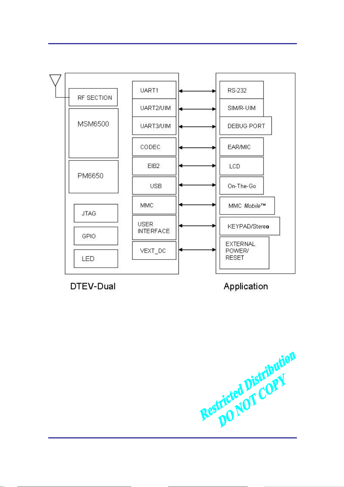
DTEV-Dual provides an external interface that includes the standard RS-232, Digital Audio, parallel
LCD Display, Keypad, Multimedia Card, R-UIM/USIM, USB-OTG, GPIO.
DTEV-Dual has the capability to power down unused circuits in order to dynamically minimize
power consumption.
All Rights Reserved.
AD-2001-06-28 Ver 1.1
-12-
Page 13

AnyDATA.NET Inc. AnyTime AnyPlace Any Wireless Data Solution
2.2 Technical Specifications
2.2.1 General Specifications
Table 2-1 General Specifications
Parameters Descriptions
External Access Code-Division-Multiple-Access (CDMA)
CDMA Protocol IS-95 A/B, IS-126, IS-637A, IS-707A, IS-2000,IS-856
Data Rate
CDMA2000 1X
1xEV-DO
System Memory 256Mbytes SDRAM and 256 Mbytes NAND Flash
Transmit/Receive Frequency Interval 45MHz for Cellular and 80MHz for PCS
Vocoder EVRC, 13kQCELP
RF technology Zero Intermediate Frequency
Number of Channel 832 for Cellular and 42 for PCS
Operating Voltage DC +3.3V ~ +4.5V BATT_INT (Pin88 and 90)
Current Consumption 1. VCC applied to VEXT_DC (Pin87 and Pin89)
Operating Temperature -30ºC ~ +60ºC
Frequency Stability ±300Hz for Cellular and ±150Hz for PCS
Antenna GSC Connector, 50ohm
Size 42mm(W) X 67mm(L) X 3.0mm(H) with case
Weight About 20g (0.7oz)
External Interface RS-232 UART, R-UIM, Parallel LCD, Keypad, MP3, MIDI, MMC
User Interface Software BREW support
Additional Function gpsOne position location solution
153 Kbps on both the forward and reverse links
Forward link: 2.4 Mbps
Reverse link: 153 Kbps
DC +4.0V to +5.25V VEXT_DC (Pin87 and Pin89)
Receive mode: 110mA
Sleep mode : less than 10mA
Busy mode: 900mA (Max)
2. VCC applied to BATT_INT (Pin88 and Pin90)
Receive mode : 110mA
Sleep mode : less than 1mA
Busy mode: 900mA (Max)
Mobile™ , USB-On-The-Go, Stereo Wireband Codec, GPIO
TM
All Rights Reserved.
AD-2001-06-28 Ver 1.1
-13-
Page 14

AnyDATA.NET Inc. AnyTime AnyPlace Any Wireless Data Solution
2.2.2 Receiver Specifications
Table 2-2 Receiver Specifications
Parameters Descriptions
Frequency Range
Cellular
Sensitivity
1xRTT
EVDO
Input Dynamic Range
1xRTT
EVDO
Single Tone Desensitization
The FER in each test shall not
exceed 1.0% with 95% confidence
Intermodulation Spurious
Response Attenuation
(Two interfering CW tones)
The FER in each test shall not
exceed 1.0% with 95% confidence
Spurious Wave Suppression Below –80dBc
869.04 ~ 893.97 MHz
1931.25 ~ 1988.75MHz
PCS
Below –104.0 dBm/1.23MHz
Below –105.5 dBm/1.23MHz
-25 dBm/1.23MHz ~ -104.0dBm/1.23MHz
-25 dBm/1.23MHz ~ -105.5dBm/1.23MHz
1xRTT
Band Classes 0 (-30dBm @900KHz and -30dBm @-900KHz):
Below –101.0 dBm/1.23MHz
Band Classes 1 (-30dBm @1250KHz and -30dBm @-1250KHz):
Below –101.0 dBm/1.23MHz
EVDO
Band Classes 0 (-30dBm @900KHz and -30dBm @-900KHz):
Below –102.4 dBm/1.23MHz
Band Classes 1 (-30dBm @1250KHz and -30dBm @-1250KHz):
Below –102.4 dBm/1.23MHz
1xRTT
Band Classes 0
Two tone (-43 dBm @900KHz and 1700KHz):
Below –101.0dBm/1.23MHz
Two tone (-32 dBm @900KHz and 1700KHz):
Below –90.0dBm/1.23MHz
Two tone (-21 dBm @900KHz and 1700KHz):
Below –79.0dBm/1.23MHZ
Band Classes 1
Two tone (-43 dBm @1250KHz and 2050KHz):
Below –101.0dBm/1.23MHz
Two tone (-32 dBm @1250KHz and 2050KHz):
Below –90.0dBm/1.23MHz
Two tone (-21 dBm @1250KHz and 2050KHz):
Below –79.0dBm/1.23MHZ
EVDO
Band Classes 0
Two tone (-43 dBm @900KHz and 1700KHz):
Below –102.4dBm/1.23MHz
Two tone (-32 dBm @900KHz and 1700KHz):
Below –91.4dBm/1.23MHz
Two tone (-21 dBm @900KHz and 1700KHz):
Below –80.4dBm/1.23MHZ
Band Classes 1
Two tone (-43 dBm @1250KHz and 2050KHz):
Below –102.4dBm/1.23MHz
Two tone (-32 dBm @1250KHz and 2050KHz):
Below –91.4dBm/1.23MHz
Two tone (-21 dBm @1250KHz and 2050KHz):
Below –80.4dBm/1.23MHZ
TM
All Rights Reserved.
AD-2001-06-28 Ver 1.1
-14-
Page 15

AnyDATA.NET Inc. AnyTime AnyPlace Any Wireless Data Solution
2.2.3 Transmitter Specifications
Table 2-3 Transmitter Specifications
Parameters Descriptions
Frequency Range
Cellular
Nominal Max Power 0.32 W (24.7dBm)
Peak Power in Operation Mode 400mW (26dBm)
Minimum Controlled Output Power Below –50dBm
Max Power Spurious
Cellular
2.2.4 gpsOne Receiver Specifications
Table 2-4 gpsOne Receiver Specifications
Parameters Descriptions
Frequency Range
C/A Code 1.023 MHz Chip Rate
Bandwidth 2.046 MHz
Modulation BPSK
Receiver Sensitivity
Without SA message
With SA message
Interference
824.04 ~ 848.97 MHz
1851.25 ~ 1908.75MHz
PCS
900KHz: Below –42dBc/30KHz
1.98MHz: Below –54dBc/30KHz
1.25MHz: Below –42dBc/30KHz
PCS
1.98MHz: Below –50dBc/30KHz
L1, 1575.42 MHz
-149dBm
-152dBm
TM
at Min At minimum C/N0 (17 dB-Hz)
CW interference
1kHz Bandwidth Interference
+
10
kHz Bandwidth Interference
VCO Phase Noise
at 100 Hz offset
at 1 KHz offset
at 10 KHz offset
at 100 KHz offset
at 2 MHz offset
–36dB
–17dB
-7dB
–50 dBc/Hz
–70 dBc/Hz
-90 dBc/Hz
-115 dBc/Hz
-140 dBc/Hz
All Rights Reserved.
AD-2001-06-28 Ver 1.1
-15-
Page 16

AnyDATA.NET Inc. AnyTime AnyPlace Any Wireless Data Solution
2.2.5 Standards
IS-95 A/B, IS-2000, IS-856: Protocol Between MS & BTS
IS-866: 3GPP2 C.S0033-0 Version 2.0: Recommended Minimum Performance Standards for CDMA2000 High
Rate Packet Data Access Terminal
IS-96A: Voice Signal Coding
IS-98A: Base MS Function
IS-98E: Recommended Minimum Performance Standards for cdma2000 Spread Spectrum Mobile Stations
IS-126: Voice Loop-Back
IS-637: Short Message Service
IS-707: Data Service
IS-657: packet data
USB 2.0 Specification and OTG Supplement: Exchanging data between a host and peripheral
TM
MMC System Specification 1.4:
ITU-T G.712: Transmission systems and media, Digital systems and networks
Built-in TCP/IP: AnyDATA proprietary software
MultiMediaCard standard
All Rights Reserved.
AD-2001-06-28 Ver 1.1
-16-
Page 17
AnyDATA.NET Inc. AnyTime AnyPlace Any Wireless Data Solution
2.3 Interface Diagram
TM
Figure 2-1 Interface Block Diagram
All Rights Reserved.
AD-2001-06-28 Ver 1.1
-17-
Page 18
AnyDATA.NET Inc. AnyTime AnyPlace Any Wireless Data Solution
3. PIN Description
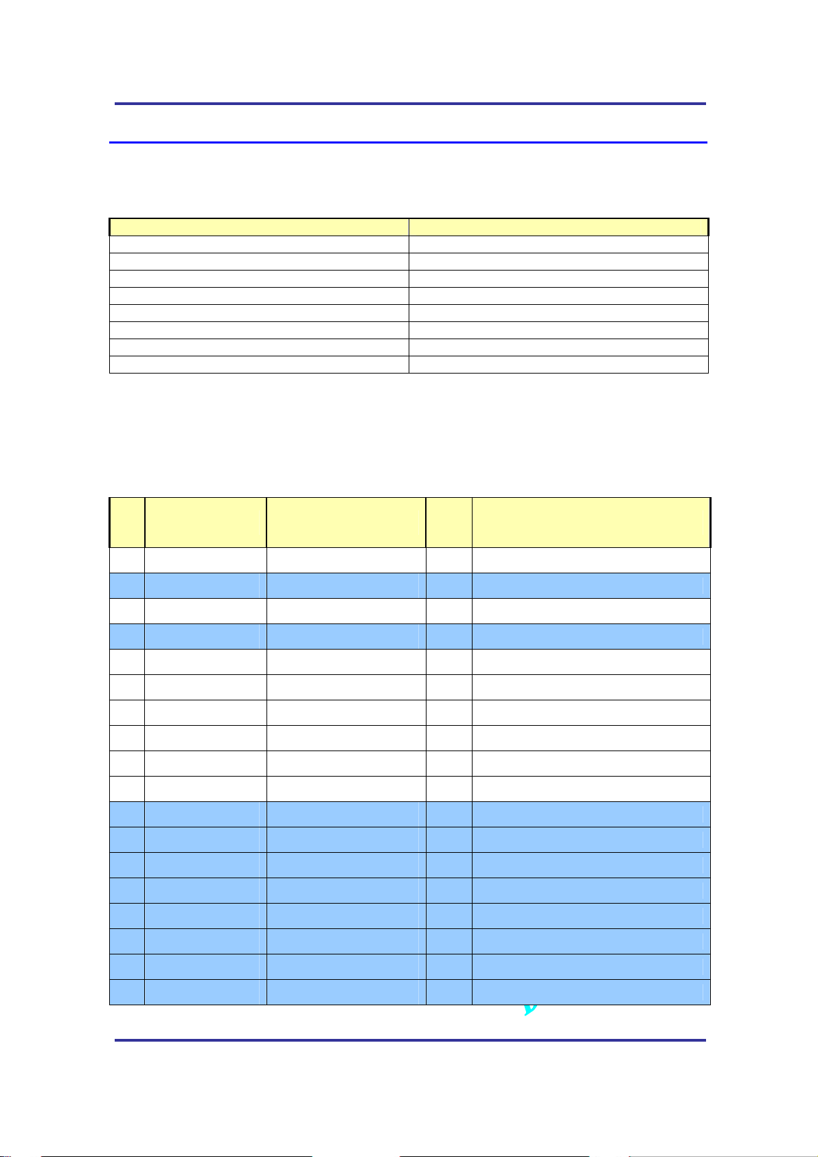
3.1 I/O Description Parameters
Table 3-1 I/O Description Parameters
Symbol Description
I
O Output
B Bi-directional
V Power/Ground
IS Input with Schmitt Trigger
BS Bi-directional Schmitt Trigger
PU Internal Pull-Up
PD Internal Pull-Down
3.2 PIN Names and Pinouts
3.2.1 100-Pin Connector
Table 3-2 100-PIN Connector Pinouts
CMOS Input
TM
Pin
Name Main Function
#
1 D2[15] EBI2_DATA15 B peripheral data bus
2 GND GROUND V
3 D2[14] EBI2_DATA14 B peripheral data bus
4 GND GROUND V
5 D2[12] EBI2_DATA12 B peripheral data bus
6 D2[13] EBI2_DATA13 B peripheral data bus
7 D2[10] EBI2_DATA10 B peripheral data bus
8 D2[11] EBI2_DATA11 B peripheral data bus
9 D2[08] EBI2_DATA08 B peripheral data bus
10 D2[09] EBI2_DATA09 B peripheral data bus
11 GND GROUND V
12 GND GROUND V
13 GPIO_39 UART1_DCD_N O
14 GPIO_64 UART1_RI_N O
Dir-
Description
Pol
Signal Ground
Analog Ground
Signal ground
Signal ground
Data carrier detect ( UART1 )
Ring indicator ( UART1 )
15 GPIO_98 UART1_RFR_N O
16 GPIO_95 UART1_TXD O
17 GPIO_44 UART1_DTR I
18 GPIO_96 UART1_RXD I
Ready for Receive ( UART1 ) same as RTS
Transmit data ( UART1 )
Data terminal ready ( UART1 )
Receive data ( UART1 )
All Rights Reserved.
AD-2001-06-28 Ver 1.1
-18-
Page 19

AnyDATA.NET Inc. AnyTime AnyPlace Any Wireless Data Solution
19 GPIO_97 UART1_CTS_N I
Clear to send ( UART1 )
TM
20 VREG_UIM VREG_RUIM O
21 UIM_P_DATA UIM_P_DATA I
22 UIM_P_RESET UIM_P_RESET O
23 UIM_P_CLK UIM_P_CLK O
24 MMC_DATA MMC_DATA B
25 MMC_CLK MMC_CLK B
26 GPIO_84 UART3_TXD O
27 MMC_CMD MMC_CMD B
28 GPIO_85 UART3_RXD I receive data, (UART3) DEBUG PORT
29 VREG_MMC VREG_AUX1 O
30 POWER_ON POWER_ON I
31 GPIO_24 LCD_LED_CONT O
32 GPIO_13 FLASH_LED_CONT O
33 GPIO_17 GPIO_17 B
34 VREG_MSME VREG_MSME O
+3V power supply to RUIM caed
Data from RUIM card
RUIM card reset
RUIM clock
GPIO_32, MultiMediaCard data
GPIO_31, MMC clock
transmit data, (UART3) DEBUG PORT
GPIO_30, MMC command
Linear regulator output intended to power
MMC circuits
POWER ON used only when to use 3.6V
1cell battery. External pull-up required
General purpose input output, LCD LED
General purpose input output, FLASH LED
General purpose input output
Regulated output of the MSME buck (step-
down) SMPS
35 VREG_AUX2 VREG_AUX2 O
36 GND GROUND V
37 GND GROUND V
38 D2[00] EBI2_DATA00 B
39 D2[01] EBI2_DATA01 B
40 D2[02] EBI2_DATA02 B
41 D2[03] EBI2_DATA03 B
42 D2[04] EBI2_DATA04 B
43 D2[05] EBI2_DATA05 B
44 D2[06] EBI2_DATA06 B
45 D2[07] EBI2_DATA07 B
46 A2[20] A2[20] O
47 A2[01] A2[01] O
48 RESOUT1 RESOUT1_N O
49 LCD2_CS LCD2_CS_N O Peripheral LCD chip select
Low dropout linear regulator output
intended to power WLAN
Signal ground
Signal ground
Data line
Data line
Data line
Data line
Data line
Data line
Data line
Data line
Address line
Address line
Reset Out
50 GPIO23 LED_FULL_CURRENT O
GPIO, Full Current LED
All Rights Reserved.
AD-2001-06-28 Ver 1.1
-19-
Page 20

AnyDATA.NET Inc. AnyTime AnyPlace Any Wireless Data Solution
51 OE2 OE2_N O
LCD Output Enable Signal
TM
52 WE2 WE2_N O
53 GPIO_62 KEYSENSE0_N I
54 GPIO_63 KEYSENSE1_N I
55 GPIO_46 KEYSENSE2_N I
56 GPIO_47 KEYSENSE3_N I
57 GPIO_48 KEYSENSE4_N I
58 GPIO_45 KYPAD_5 I
59 GPIO_53 KYPAD_4 I
60 GPIO_52 KYPAD_3 I
61 GPIO_51 KYPAD_2 I
62 GPIO_50 KYPAD_1 I
63 GPIO_49 KYPAD_0 I
64 GPIO_80 AUX_PCM_CLK B
65 GPIO_81 AUX_PCM_SYNC O
LCD Write Enable Signal
Key sense input
Key sense input
Key sense input
Key sense input
Key sense input
GPIO, Keypad input
GPIO, Keypad input
GPIO, Keypad input
GPIO, Keypad input
GPIO, Keypad input
GPIO, Keypad input
PCM clock for auxiliary CODEC port
or IDLE LED output. Default is LED
PCM data strobe for auxiliary CODEC port
or Traffic LED output. Default is LED
66 GPIO_82 AUX_PCM_DIN I
67 GPIO_21 AMUX_IN1 I External inputs to the analog multiplexer
68 GPIO_83 AUX_PCM_DOUT O PCM data output for auxiliary CODEC port
69 GPIO_05 AMUX_IN2 I External inputs to the analog multiplexer
70 GPIO_37 COVER_DET B
71 VIB_DRV_N VIB_DRV_N O
72 GPIO_42 PS_HOLD O
73 SPK_M SPRK_OUT_M O Speaker driver output (-)
74 KYD_BAKLIGHT KEY_BAKLIGHT O
75 SPK_P SPRK_OUT_P O Speaker driver output (+)
76 GND GROUND V
77 GND GROUND V
78 EAR_DET EAR_DET1 I
79 HPH_R HPH_R O Stereo headphone output, Right
80 EAR10_P EAR10_P O Earphone 1 amplifier output (+)
PCM data input for auxiliary CODEC port
or SMS LED output. Default is LED
General purpose input output
VIBRATOR_DRV output
POWER LED Enable
KYD_BAKLIGHT output
Signal ground
Signal ground
GPIO, EAR Jack Detect
81 EAR10_M EAR10_M O Earphone 1 amplifier output (-)
82 MIC1_P MIC1_P I
External Mic (+) input
All Rights Reserved.
AD-2001-06-28 Ver 1.1
-20-
Page 21

AnyDATA.NET Inc. AnyTime AnyPlace Any Wireless Data Solution
83 MIC2_P MIC2_P I
Ear Jack Mic (+) input
TM
84 GND GROUND V
85 GND GROUND V
86 VPH_PWR VPH_PWR O
87 VBATT_DC VEXT_DC I
88 VBATT_INT VBATT_INT I
89 VEXT_DC VEXT_DC I
90 VBATT_INT VBATT_INT I
91 GPIO_29 USB_VBUS I
92 USB_OE_TP_N USB_CON_D_M B USB differential data minus (-)
93 USB_SEO_VM USB_CON_ID I Not in use
94 USB_DAT_VP USB_CON_D_P B USB differential dada minus (+)
95 MIC1_M MIC1_M I
96 VPH_PWR VPH_PWR O
Signal Ground
Signal ground
+3.3V ~ +4.2V power supply to peripheral
device
External DC input
Battery input
External DC input
Battery input
+5Vdc input or output depending upon the
type of peripheral device connected.
Default is input
External Mic (-) input
+3.3V ~ +4.2V power supply to peripheral
device
97 HPH_L HPH_L O Stereo headphone output, Left
98 N.C GPIO_35 B
99 GND GROUND V
100 GND GROUND V
General purpose input output
Signal ground
Signal ground
All Rights Reserved.
AD-2001-06-28 Ver 1.1
-21-
Page 22
AnyDATA.NET Inc. AnyTime AnyPlace Any Wireless Data Solution
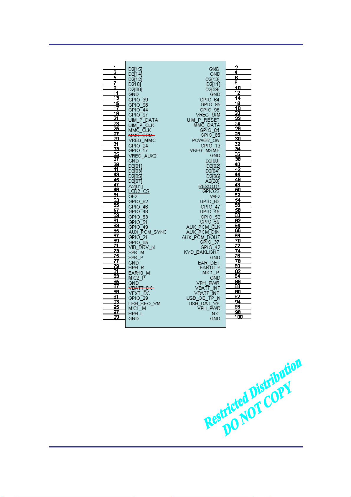
3.2.2 100-Pin Connector Pin-out (Top view)
MMC_CMD
TM
VEXT_DC
Figure 3-1 100-PIN Connector Pinouts
Notes:
* Pin16 and Pin18 can be used as a debugging port if USB is used as primary data. We strongly
recommend that the user have a 3-pin connector or 3 test points on their board, so that one can easily
monitor and diagnose their module.
LEAVE UNUSED PINS OPEN AT ALL TIMES
All Rights Reserved.
AD-2001-06-28 Ver 1.1
-22-
Page 23

AnyDATA.NET Inc. AnyTime AnyPlace Any Wireless Data Solution
TM
4. Interface Descriptions
4.1 Overview
This chapter covers information required to convert the DTEV-Dual into a subscriber unit application.
In addition, some of the internal blocks of the device are described. Understanding these internal blocks is
necessary for one to completely grasp the functions of the various interfaces.
This chapter discusses the interface to the major blocks of the DTEV-Dual as shown in the following
figure. These blocks include:
Power Up
Power Down Registration Protocol for CDMA device
Stereo Wideband CODEC Interface
UART Interface
General Purpose Interface
User Interface
External Bus Interface II
USB Interface
LED Interface
RF Interface
All Rights Reserved.
AD-2001-06-28 Ver 1.1
-23-
Page 24
AnyDATA.NET Inc. AnyTime AnyPlace Any Wireless Data Solution
TM
4.2 Powering Up the Module
There are two ways to power up the module and customers may choose one of the two ways to power
up DTEV-Dual module.
4.2.1 External Supply
If the customers don’t need to save current in sleep mode, which is around 10mA, supplying voltage to
VEXT_DC (Pin 87 and Pin89) is recommended. When the input voltage from +4V to +5.25V is supplied,
DTEV-Dual will automatically start its power-on process and finish it within 2 seconds. In this case, using
a regulator with an enable pin is highly recommended so that the customer can reset the module using the
enable pin if software lock-up symptoms are found.
If a customer needs to use charging circuit built in the module, apply +5.0V DC to VEXT_DC(Pin87
and Pin89) and connect a +3.6V 1-cell lithium-ion battery to BATT_INT(Pin88 and 90).
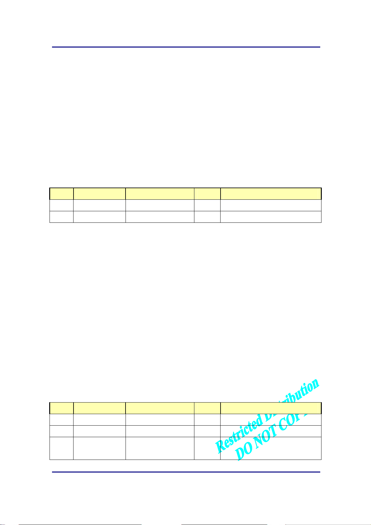
Table 4-1 Eternal Supply Pinouts
Pin # Pin Name Main Function Type Description
87 VEXT_DC VEXT_DC I External DC input
89 VEXT_DC VEXT_DC I
External DC input
4.2.2 Keypad Power On and Supply Input to BATT_INT
If the customers need to get their device to operate in a very low sleep current mode, supplying
voltage to BATT_INT (Pin 88 and 90) is recommended.
When the input voltage from +3.3V to +4.5V is supplied to BATT_INT (Pin88 and 90) and
POWER_ON goes to Low from High, power on sequence is initialed. For a successful power on sequence,
POWER_ON(Pin30) must stay Low for more than 500msec and less than 2sec).
To power off the module, have POWER_ON(Pin 30) stay low for more than 2sec and less than
4sec and then the voltage in BATT_INT may or may not be removed.
If Vcc is supplied thru a regulator or a DC/DC converter to BATT_INT(Pin88 and 90), using
one with an enable pin is highly recommended so that the customer can shut off the power to the module
using the enable pin if software lock-up symptoms are found. If the modem is locked up, low assertion of
POWER_ON (Pin 30) won’t power on or off the module. If Vcc is supplied directly from a battery, having
a FET between the output of a battery and VBATT_INT(Pin88 and Pin90) is recommended that the
customer can shut off the power to DTEV-Dual using the FET switch.
Table 4-2 Battery Supply Pinouts
Pin # Pin Name Main Function Type Description
88 VBATT_INT VBATT_INT I Battery plus (+) input
90 VBATT_INT VBATT_INT I
30 POWER_ON POWER_ON I
Battery plus (+) input
POWER ON used only when to use
+3.6V 1-cell battery. External pull-up
to
+3V to +4.5V thru 100kohm resistor.
All Rights Reserved.
AD-2001-06-28 Ver 1.1
-24-
Page 25
AnyDATA.NET Inc. AnyTime AnyPlace Any Wireless Data Solution
TM
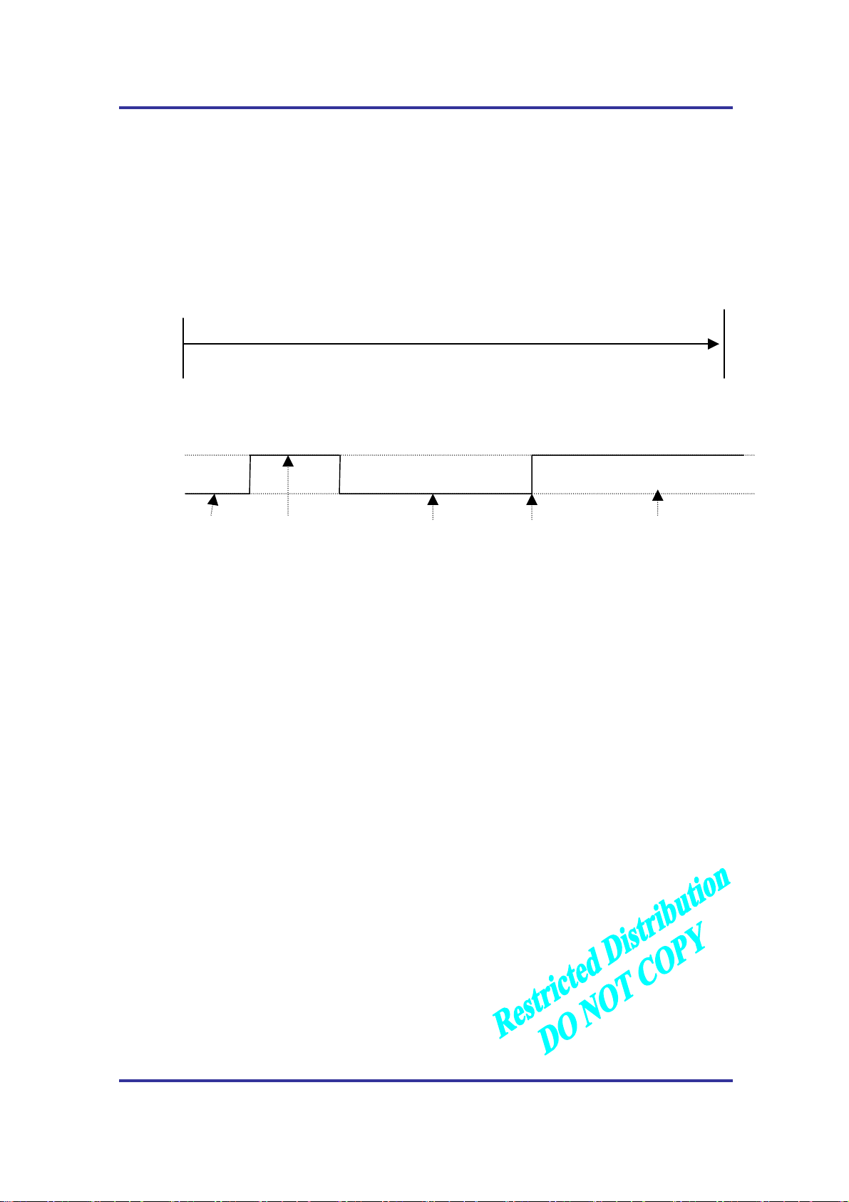
4.3 Power Down Registration Protocol for CDMA device
Before DTEV-Dual is powered off, it has to send power down registration message to the
CDMA base station to help the base station to maximize its capacity. Depending on air interface
environment, it may take up to 12 seconds according to CDMA technical standard.
4.3.1 Using AT command (When Vcc is applied to VEXT_DC)
Device connected to DTEV-Dual
4.3.2 Using POWER_ON (Pin 30) (Only when Vcc is applied to BATT_INT)
HIGH
LOW
Before powering off DTEV-Dual, send “AT+POWEROFF” to DTEV-Dual.
After waiting for 12 seconds, the host device may shut down the power to DTEV-Dual
Booting stage. In normal operation
Powering the module off. 2 sec
T1
T1+12sec. Shut off the Vcc to
DTEV-Dual
DTEV-Dual
Status of POWER_ON (Pin 30)
All Rights Reserved.
AD-2001-06-28 Ver 1.1
-25-
Page 26
AnyDATA.NET Inc. AnyTime AnyPlace Any Wireless Data Solution
TM
4.4 Stereo Wideband CODEC Interface
With the integrated microphone and earpiece amplifier including CODEC, the DTEV-Dual
module interfaces directly, either differential or single-ended, to the microphone and earpiece.
The audio features in the module are
- Two microphone inputs
- Two earphone outputs and one auxiliary audio output.
4.4.1 Microphone and earphone Interface
The module contains analog audio interface circuitry. The contained audio interface supports all of the
required conversation and amplification stages for the audio front end.
The audio interface includes the amplification stages for both the microphone and earphone.
The module supports audio outputs with its variable gain audio as volume control can be used for
audio alerts or speaker phone. The speaker driver has programmable gain, turn-on time, and muting, and
operates as a differential device delivering a volume-controlled 500mW to an external 8-Ohm speaker.
The EAR10 and MIC1P are typically used for the handset ear-piece/mic.
The EAR_JACK+ and MIC2P are typically used for the ear-jack.
Table 4-4.1 Analog Audio Pinouts
Pin # Pin Name Main Function Type Description
73 SPK_M SPRK_OUT_M O Loud speaker output (-)
75 SPK_P SPRK_OUT_P O Loud speaker output (+)
80 EAR10_P EAR10_P O Ear-piece output (+)
81 EAR10_M EAR10_M O Ear-piece output (-)
82 MIC1_P MIC1_P I Mic. (+) input
95 MIC1_M MIC1_M I Mic. (-) input
78 EAR_DET EAR_DET1 I EAR/MIC Set Detect*
* EAR_DET checks to see if a headset has been connected to the ear-jack. When there is no headset
connected to the ear-jack, the audio path thru an ear-jack is disconnected and ear-piece/mic. is connected.
Setting EAR_DET to HIGH disconnects ear-jack and connects ear-piece/mic.
All Rights Reserved.
AD-2001-06-28 Ver 1.1
-26-
Page 27

AnyDATA.NET Inc. AnyTime AnyPlace Any Wireless Data Solution
TM
Table 4-4.1.1Speaker Driver Performance Specifications
Parameter Comments Min Ty p Max Unit Notes
Input frequency range 0.20 20 kHz
Input resistance Differential 60 72 86 k
Input drive level V
Output power (P
Power efficiency at P
) THD < 0.5% 500 mW 2
rated
50 %
rated
RMS
Programmable amplifier gain -16 +12 dB 3
Amplifier gain error -1 +1 dB
Amplifier gain flatness 20 Hz to 20 kHz -0.5 +0.5 dB
Output referred noise
G = -16 dB
G = -12 dB
G = -8 dB
G = -4 dB
G = 0 dB
G = +4 dB
G = +8 dB
G = +12 dB
Output bandwidth at P
V
= 0V,
in
20 Hz – 20 kHz,
8 ohm Load
16
16
17
18
23
30
44
66
8 load, 12dB gain 20 kHz 5
rated
V
RMS
V
RMS
V
RMS
V
RMS
V
RMS
V
RMS
V
RMS
V
RMS
4
Output offdet voltage -40 +40 mV 6
THD + noise 5 %
Power supply rejection ratio
F = 20 Hz to 100 Hz
F = 100 Hz to 5 kHz
F = 5 kHz to 15 kHz
F = 15 kHz to 20 kHz
Turn-on time delay
Short delay
Long delay
Pop and click levels During power, gain, mute
= 0V,
V
in
V
= 3.6V + 100 mV
DD
RMS
55
65
55
50
10
12.5
100
dB
dB
dB
dB
ms
125
ms
7
11 mVPK 8
transitions
Mute suppression V
= 2 V
in
80 dB
RMS
Quiescent current 6.2 mA 6
All Rights Reserved.
AD-2001-06-28 Ver 1.1
-27-
Page 28
AnyDATA.NET Inc. AnyTime AnyPlace Any Wireless Data Solution
4.4.2 Stereo Headphone Interface
Table 4-4.2 Stereo Headphone Interface
Pin # Pin Name Main Function Type Description
83 MIC2_P MIC2_P I Ear-Mic Jack input *
TM
78
EAR_DET EAR_DET1
I EAR/MIC Set Detect **
79 HPH_R HPH_R O Stereo headphone output, Right
97 HPH_L HPH_L O Stereo headphone output, Left
Note:
* MIC2, along with being a microphone input, checks to see if the user has pressed the headset key, which
allows the user to connect to or disconnect from a call. This pin is internally pulled high and is therefore
normally in the high state. To activate this input and connect to or disconnect from a call, the user must set
the MIC2 pin to a low state for 100ms to 200ms.
** EAR_DET checks to see if a headset has been connected to the ear-jack. When there is no headset
connected to the ear-jack, the audio path thru an ear jack is disconnected. When a headset is connected to
the ear-jack, audio path is opened. To simulate a headset connected to the ear-jack, the user must apply
LOW signal to the EAR_DET pin for as long as the user wants the audio path thru ear-jack to be kept
open
4.4.3 Digital PCM Interface
The Digital PCM CODEC interface is used for the car-kit audio system. This interface is
optional. External CODEC interface signals are listed below:
Table 4-4.3 Digital CODEC Pinouts
Pin # Pin Name Main Function Type Description
64 GPIO_80 AUX_PCM_CLK B
65 GPIO_81 AUX_PCM_SYNC O
66 GPIO_82 AUX_PCM_DIN I
68 GPIO_83 AUX_PCM_DOUT O
PCM clock for auxiliary CODEC port
PCM data strobe for auxiliary CODEC port
PCM data input for auxiliary CODEC port
PCM data output for auxiliary CODEC port
This feature is not implemented but can be added, please contact [email protected]
for technical support.
4.4.4 Stereo DAC Interface
DTEV-Dual supports DAC interface to an external stereo DAC for playing stereo sound or
music (MP3 and MIDI, for example). This interface consists of four signals: serial bit clock (SDAC_CLK),
left/right select (SDAC_L_R_N), serial data (SDAC_DOUT), and master clock (SDAC_MCLK).
All Rights Reserved.
AD-2001-06-28 Ver 1.1
-28-
Page 29
AnyDATA.NET Inc. AnyTime AnyPlace Any Wireless Data Solution
Table 4-4.4 Stereo DAC Pinouts
Pin # Pin Name Main Function Type Description
TM
64 GPIO_80 AUX_PCM_CLK O
65 GPIO_81 AUX_PCM_SYNC O
66 GPIO_82 AUX_PCM_DIN O
68 GPIO_83 AUX_PCM_DOUT O
SDAC_SCK
SDAC_L_R_N
SDAC_MCLK
SDAC_DOUT
This feature is not implemented but can be added, please contact [email protected] for technical support
4.5 UART Interface
The Universal Asynchronous Receiver Transmitter (UART) communicates with serial data that
conforms to the RS-232 Interface protocol. The module has 3 UARTs which provides 2.85 V CMOS level
outputs and 2.85V CMOS input levels. All the control signals of the RS-232 are active low, however the
data signals, RXD and TXD, are active high.
UART1 which has 512 bytes for Tx and Rx FIFO, supports high speed data communication up to
230.4kbps, program download and diagnostic monitor function.
UART2 and 3 which 64 bytes for T/Rx FIFO, support low speed data communication up to 115.2kbps,
program download and diagnostic monitor function.
The UART features hardware handshaking, programmable data sizes, programmable stop bits, and odd,
even, no parity.
4.5.1 UART1 interface
Table 4-5.1 UART1 Interface Pinouts
Pin # Pin Name Main Function Type Description
13 GPIO_39 UART1_DCD_N O
Data carrier detect control input
( UART1 )
14 GPIO_64 UART1_RI_N O Ring indicator control input ( UART1 )
15 GPIO_98 UART1_RFR_N O Ready for Receive ( UART1 )
16 GPIO_95 UART1_TXD O Transmit data output ( UART1 )
17 GPIO_44 UART1_DTR I
Data terminal ready control output
( UART1 )
18 GPIO_96 UART1_RXD I Receive data input ( UART1 )
19 GPIO_97 UART1_CTS_N I Clear to send control input ( UART1 )
Leave unused Pins open.
This feature is not implemented but can be added, please contact [email protected] for technical support.
All Rights Reserved.
AD-2001-06-28 Ver 1.1
-29-
Page 30
AnyDATA.NET Inc. AnyTime AnyPlace Any Wireless Data Solution
TM
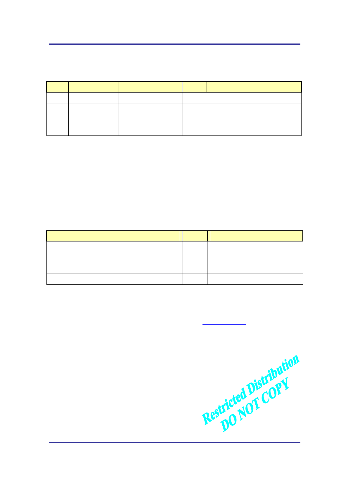
4.5.2 UART2 R-UIM interface
The UART2 supports R-UIM interface.
Table 4-5.2 UART2 Interface Pinouts
Pin # Pin Name Main Function Type Description
20 VREG_UIM VREG_UIM O +3.0V power supply to RUIM card
21 UIM_P_DATA UIM_P_DATA I Data from RUIM card
22 UIM_P_RESET UIM_P_RESET O RUIM card reset
23 UIM_P_CLK UIM_P_CLK O RUIM clock
Leave unused Pins open.
If a customer wants to use R-UIM card, UART2 can’t be used as UART.
This feature is not implemented but can be added, please contact [email protected] for technical support.
4.5.3 UART3 Debug Port Interface
The UART3 is used to monitor and diagnose the status of the DTEV-Dual. It is strongly recommended
for the user to have the following UART3 pins connected to an extra connector or to test points, in order to
easily troubleshoot any problems with the module.
Table 4-5.3 UART3 Interface Pinouts
Pin # Pin Name Main Function Type Description
26 GPIO_84 UART3_TXD O Transmit data output, DEBUG PORT
28 GPIO_85 UART3_RXD I
16 GPIO_95 UART1_TXD O
18 GPIO_96 UART1_RXD I
Receive data input , DEBUG PORT
Transmit data output, DEBUG PORT
Receive data input , DEBUG PORT
If USB is used for primary data, use Pin16 and Pin18 for debugging.
If UART1 is used for primary data and USB is not used, use Pin26 and 28 for debugging.
Leave unused Pins open.
This feature is not implemented but can be added, please contact [email protected]
for technical support.
4.5.4 USB Interface
The module
contains Universal Serial Bus (USB) interface to provide an efficient interconnect
between the mobile phone and a personal computer (PC).It can act as a USB peripheral device, supporting
low speed 1.5 Mbps and full speed 12Mbps connections. In host mode, the module supplies VBUS with
+5Vdc at up to 25mA.
This module is USB V1.1 comparable.
All Rights Reserved.
AD-2001-06-28 Ver 1.1
-30-
Page 31

AnyDATA.NET Inc. AnyTime AnyPlace Any Wireless Data Solution
Table 4-5.4 USB Interface Pinouts
Pin # Pin Name Main Function Type Description
+5Vdc input or output depending upon
91 GPIO_29 USB_VBUS I
92 USB_OE_TP_N USB_CON_D_M B
the type of peripheral device connected.
Default in input.
Differential Data minus (-)
TM
93 USB_SE0_VM USB_CON_ID I
94 USB_DAT_VP USB_CON_D_P B
USB host feature is not implemented, please contact [email protected] for technical support.
Not in use
Differential Data plus (+)
4.6 General Purpose Interface
The general purpose interface is user-definable bi-directional pin. It can be configured as an
interrupt source. In addition, the GPIO pin can be used as output control pin from the module. The user
can define this pin properly as following.
Table 4-6 General Purpose Interface Pinouts
Pin # Pin Name Main Function Type Description
Programmable pull.
33 GPIO_17 GPIO_17 B
98 NC GPIO_35 B
This pin can be programmed to No Pull,
Pull Up, or Pull Down.
Programmable pull.
This pin can be programmed to No Pull,
Pull Up, or Pull Down.
All Rights Reserved.
AD-2001-06-28 Ver 1.1
-31-
Page 32
AnyDATA.NET Inc. AnyTime AnyPlace Any Wireless Data Solution
TM
4.7 User Interface
4.7.1 Keypad
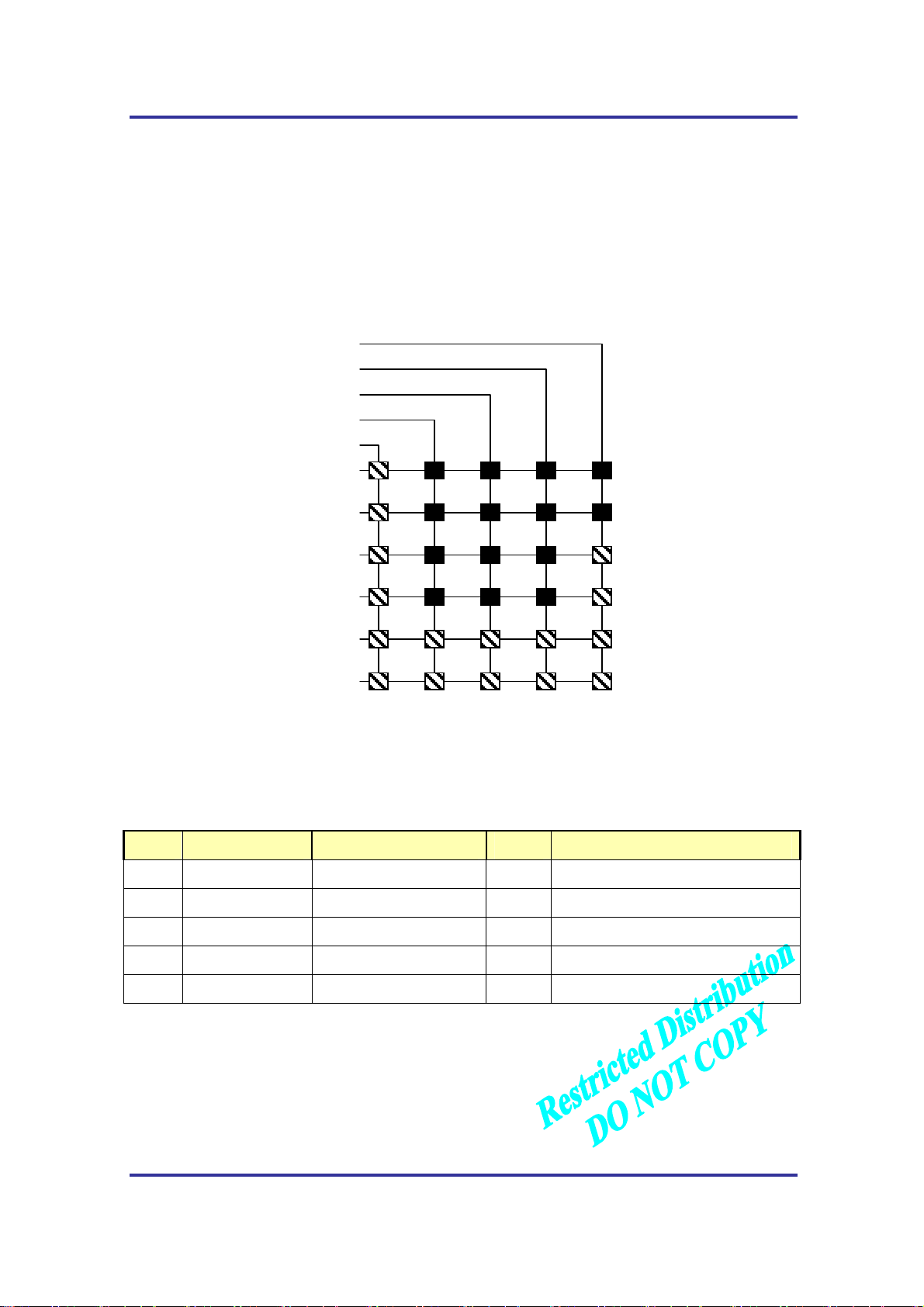
The keypad interface consists of a 5 X 6 matrix pattern. The 5-KEYSENSE/[4:0] pins are used to
connect a matrix keypad to the module. The KEYSENSE/ pins are active low.
The 6-KEYPAD pins are necessary to construct the other side of the matrix. These KEYPAD pins
must be active high in order for the keypad matrix to work properly. The general keypad matrix is shown
below:
KEYSENSE0
KEYSENSE1
KEYSENSE2
KEYSENSE3
KEYPAD00
KEYPAD01
KEYPAD02
KEYPAD03
KEYPAD04
KEYPAD05
# 0 * SEND
9 8 7 END
6 5 4
3 2 1
Reserve
Figure 4-7.1 Keypad Matrix
d
Table 4-7.1.1 Keysense GPIO Pinouts
Pin # Pin Name Main Function Type Description
53 GPIO_62 KEYSENSE0_N
I
Key sense input
54 GPIO_63 KEYSENSE1_N I Key sense input
55 GPIO_46 KEYSENSE2_N I Key sense input
56 GPIO_47 KEYSENSE3_N I
57 GPIO_48 KEYSENSE4_N I
Key sense input
Key sense input
All Rights Reserved.
AD-2001-06-28 Ver 1.1
-32-
Page 33

AnyDATA.NET Inc. AnyTime AnyPlace Any Wireless Data Solution
Table 4-7.1.2 Keypad GPIO Pinouts
Pin # Pin Name Main Function Type Description
TM
58 GPIO_45 KYPAD_5
I
GPIO, Keypad input
59 GPIO_53 KYPAD_4 I GPIO, Keypad input
60 GPIO_52 KYPAD_3 I GPIO, Keypad input
61 GPIO_51 KYPAD_2 I GPIO, Keypad input
62 GPIO_50 KYPAD_1 I GPIO, Keypad input
63 GPIO_49 KYPAD_0 I GPIO, Keypad input
DTMF
When key is pressed, CDMA Module generates standard DTMF tone and sends it to the local
audio path (speaker). If the Mobile station is in traffic state, the CDMA Module sends DTMF Message to
the Base Station and to the local audio path (speaker) at the same time. The network will deliver the
analog DTMF tone or DTMF Message to its final destination.
This feature is not implemented but can be added, please contact [email protected]
for technical support. .
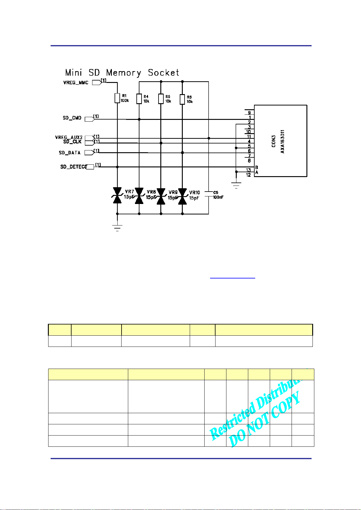
4.7.2 MultiMediaCard controller
DTEV-Dual contains a MultiMediaCard (MMC) controller that provides a link between the
ARM bus master and the MultiMediaCard bus for storing digital music, games, address books and photos.
The SD card supports a 1-bit SD bi-directional bus mode. SD bus pins are CLK, CMD and DAT in 1-bit
mode and CLK, CMD, and DAT[0:3] in 4-bit mode. The MultiMediaCard also supports the 1-bit bi-
directional MMC bus mode that has CLK, CMD, and DAT bus pins. The CMD and DAT pins are bi-
directional on the SD 1-bit, SD 4-bit, and MMC 1-bit. DTEV-Dual can’t support SD 4-bit mode. MMC
version 3.31 is supported for the ROM class and R/W MMCs. SD Memory Card Physical Layer
Specification Version 1.01 is supported in SD bus mode.
Table 4-7.2 MultiMediacatd Controller Pinouts
Pin # Pin Name Main Function Type Description
24 MMC_DATA MMC_DATA B GPIO_32, MultiMediaCard data
25 MMC_CLK MMC_CLK O GPIO_31, MMC clock
27 MMC_CMD MMC_CMD B GPIO_30, MMC command
29 VREG_MMC VREG_MMC O +2.85V
35 VREG_AUX2 VREG_AUX2 O +2.85V
68 GPIO_INT22 SD_DETECT I SD/MMC detect. Low detection
All Rights Reserved.
AD-2001-06-28 Ver 1.1
-33-
Page 34
AnyDATA.NET Inc. AnyTime AnyPlace Any Wireless Data Solution
TM
Figure 4-7.2 MMC Bus Circuitry Diagram
This feature is not implemented but can be added, please contact [email protected]
for technical support.
4.7.3 Vibration Motor Driver
DTEV-Dual supports silent incoming-call alarms with its vibration motor driver.
Table 4-7.3.1 Vibration Motor Driver Pinouts
Pin # Pin Name Main Function Type Description
71 VIB_DRV_N VIB_DRV_N O VIBRATOR_DRV output
Table 4-7.3.2 Vibration motor driver performance specifications
Parameter Comments Min Ty p Max Unit Notes
Output voltage (Vm) error
Gain error
V
≥ 3.2V; Im=0 to 175mA;
DD
Vm setting = 1.2 to 3.1V
-6
+6
%
1
Offset error
Short circuit current VIB_DRV_N (pin25) = V
-60
225 500 mA
DD
+60
mV
Driver bias current Im= 175mA 78 2
Driver leakage current 100 nA
All Rights Reserved.
AD-2001-06-28 Ver 1.1
-34-
Page 35

AnyDATA.NET Inc. AnyTime AnyPlace Any Wireless Data Solution
TM
Notes:
1. The vibration motor driver circuit is a low-side driver. The motor is connected directly to VDD and the
voltage across the motor is : Vm = VDD – V
where V
out
is the PM6650 voltage at pin25 (VIB_DRV_N).
out
2. Driver bias current is the change in IDD when the motor driver is turned on less the motor current.
This feature is not implemented but can be added, please contact [email protected] for technical support.
4.7.4 LED Interface
Table 4-7.4 LED Pinouts
PIN NUMBER
64
65
66
72
Above pins can not drive LED directly. Must use driver ICs to drive LEDs
USE REMARK
Idle LED
Traffic LED
SMS LED
Power On LED
High Enable, High indicates
“The device is in CDMA service area”
High Enable, High indicates
“The device is in CDMA Traffic state”
High Enable High indicates
“The device has received SMS message
High Enable High indicates
“The device is turned on”
All Rights Reserved.
AD-2001-06-28 Ver 1.1
-35-
Page 36

AnyDATA.NET Inc. AnyTime AnyPlace Any Wireless Data Solution
TM
4.8 External Bus Interface II ( or LCD Interface )
The External bus interface II supports the parallel LCD interfaces. The port mapped or memory
mapped (16-bit interface and 8-bit devices) parallel LCD device could be connected to chip select
LCD2_CS_N in EBI2. The maximum address space per chip select is 2 Megabyte. Direct access to the
LCD driver is not applicable.
Table 4-8 LCD Interface Pinouts
Pin # Pin Name Main Function Type Description
1 D2[15] EBI2_DATA15 B Data line
3 D2[14] EBI2_DATA14 B Data line
5 D2[12] EBI2_DATA12 B Data line
6 D2[13] EBI2_DATA13 B Data line
7 D2[10] EBI2_DATA10 B Data line
8 D2[11] EBI2_DATA11 B Data line
9 D2[08] EBI2_DATA08 B Data line
10 D2[09] EBI2_DATA09 B Data line
38 D2[00] EBI2_DATA00 B Data line
39 D2[01] EBI2_DATA01 B Data line
40 D2[02] EBI2_DATA02 B Data line
41 D2[03] EBI2_DATA03 B Data line
42 D2[04] EBI2_DATA04 B Data line
43 D2[05] EBI2_DATA05 B Data line
44 D2[06] EBI2_DATA06 B Data line
45 D2[07] EBI2_DATA07 B Data line
46 A2[20] A2[20] O Address line
47 A2[01] A2[01] O Address line
49 LCD2_CS LCD2_CS_N O
Peripheral LCD Chip Select
48 RESOUT1 RESOUT1_N O Reset Out
51 OE2 OE2_N O Output Enable Signal
52 WE2 WE2_N O Write Enable Signal
This feature is not implemented but can be added, please contact [email protected] for technical support.
All Rights Reserved.
AD-2001-06-28 Ver 1.1
-36-
Page 37
AnyDATA.NET Inc. AnyTime AnyPlace Any Wireless Data Solution
4.9 Antenna Interface
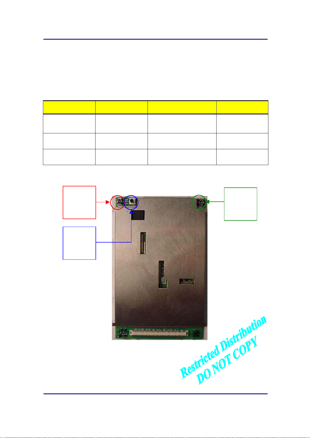
DTEV-Dual supports antenna diversity for CDMA signal reception, MS-Assisted GPS, MS-Based
GPS, simultaneous GPS, standalone GPS using secondary RF chain.
Table 4-9 Required Antenna Type
INTENDED
OPERATION
- CDMA with Diversity
- GPS
- CDMA with Diversity
- No GPS support
PRIMARY ANTENNA
800/1900MHz Dual Band
800/1900MHz Dual Band
SECONDARY ANTENNA REMARK
800/1900/1575MHz Tri Band
800/1900MHz Dual Band
CDMA Diversity and
GPS support
Optimized for CDMA
Signal Reception
TM
- CDMA without Diversity
- GPS
Primary
Antenna
Connector
RF Test
Switch
Connector
800/1900MHz Dual Band
1575.42MHz Single Band
Optimized for GPS
Signal Reception
Secondary
Antenna
Connector
All Rights Reserved.
AD-2001-06-28 Ver 1.1
-37-
Page 38
AnyDATA.NET Inc. AnyTime AnyPlace Any Wireless Data Solution
TM
5. Electrical Specifications
5.1 DC Electrical Specifications
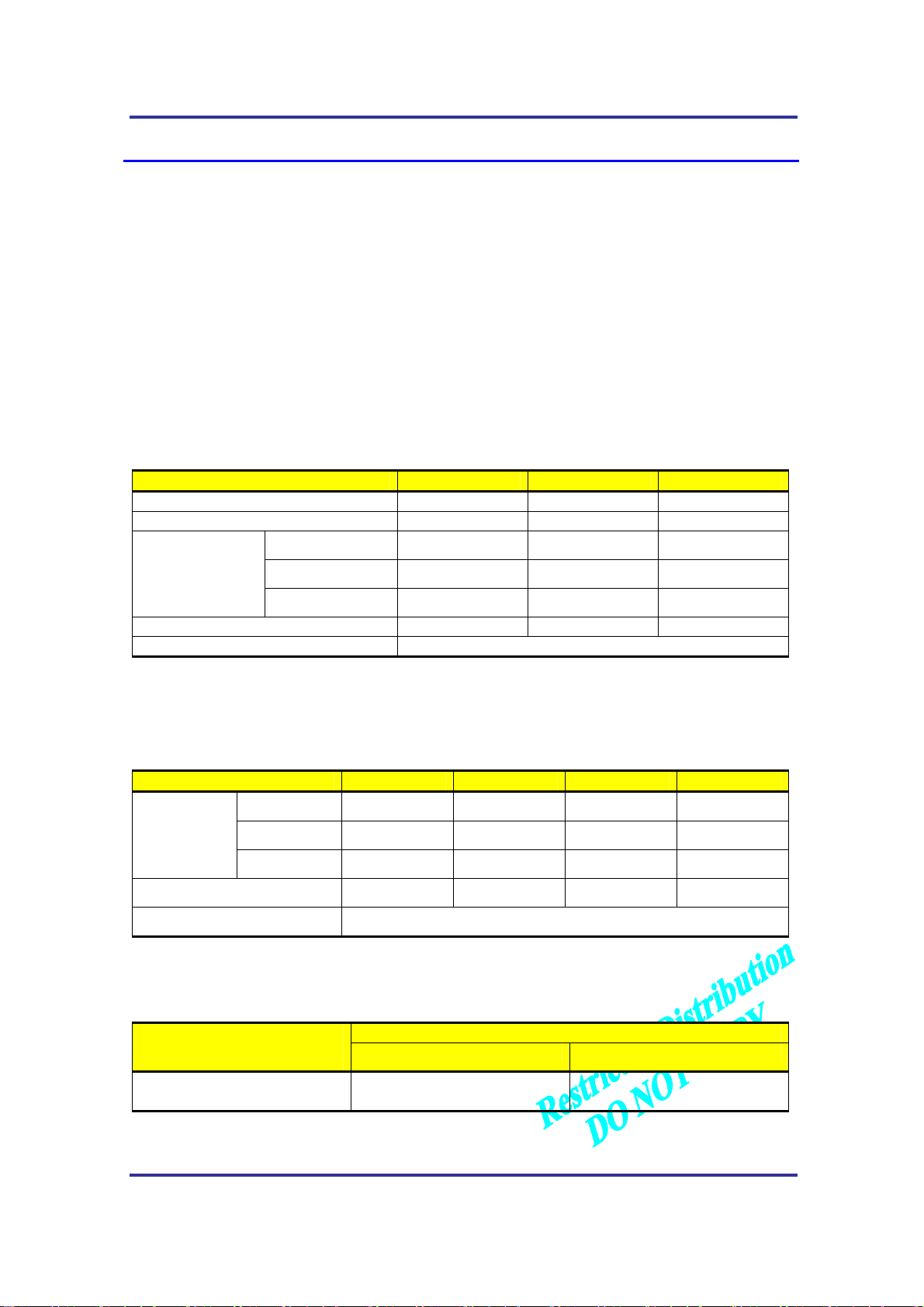
5.1.1 Absolute Maximum Ratings
Operating the module under conditions that exceed those listed in the Absolute Maximum Ratings
table may result in damage to the module.
Absolute Maximum Ratings should be considered as limiting values. The module may not function
properly and should not be operated if any one of the parameters is not within its specified operating range.
Table 5-1 Absolute Maximum Ratings
PARAMETER MIN MAX
Storage Temperature
Voltage apply to any Input or output pin
VEXT_DC
-50 +85 ºC
-0.5 +3.5 V
-0.5 +5.5 V
UNITS
Supply Voltage
Initializing Current
Drop
VBATT_INT -0.5 +4.5 V
USB_VBUS -0.5 +5.25 V
250 mA
No damages after 60-Inch drop over concrete floor
5.1.2 Recommended Operating Conditions
Table 5-1.2 Recommended Operating Conditions
PARAMETER MIN TYP MAX
VEXT_DC +4.0 +5.0 +5.25 V
Supply Voltage
Operating Temperature -30 +60 ºC
Operating Humidity
VBATT_INT +3.3 +4.0 +4.5 V
USB_VBUS +4.4 +5.0 +5.25 V
95% (50°C) Relative Humidity
UNITS
5.1.3 Power Consumption
Table 5-1.3 Power Consumption
CONVERSATION
(Busy)
900mA (MAX)
Rx Sleep
110mA
STANDBY
VEXT_DC : 10mA
BATT_INT : 1mA
All Rights Reserved.
AD-2001-06-28 Ver 1.1
-38-
Page 39
AnyDATA.NET Inc. AnyTime AnyPlace Any Wireless Data Solution
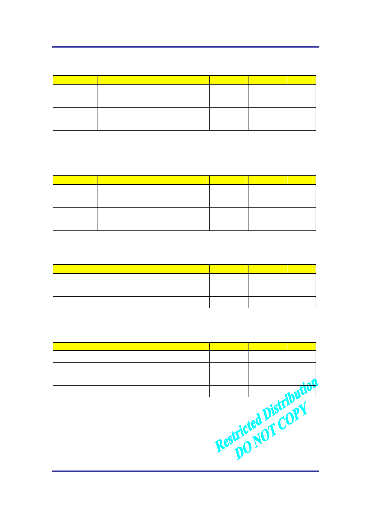
5.1.4 Serial Interface Electrical Specifications
Table 5-1.4 Serial Interface Electrical Specifications
PARAMETER DESCRIPTION MIN MAX
VIH
High-level input voltage, CMOS/Schmitt 1.7 3.3 Volts
UNITS
TM
VIL
VOH
VOL
Low-level input voltage, CMOS/Schmitt –0.3 0.94 Volts
High-level output voltage, CMOS 2.25
Low-level output voltage, CMOS 0
2.85
0.45 Volts
Volts
5.1.5 Multi-Purpose Pin Specifications
5.1.5.1 Multi-Purpose Pin Configured
Table 5-1.5.1 Multi-Purpose Pin Configured
PARAMETER DESCRIPTION MIN MAX
VIH
VIL
VOH
VOL
High-level input voltage 1.7 3.0 Volts
Low-level input voltage –0.3 0.94 Volts
High-level output voltage 2.25
Low-level output voltage 0
2.85 Volts
0.45 Volts
UNITS
5.1.5.2 Multi-Purpose Pin Configured as a Bidirectional I/O
Table 5-1.5.2 Multi-Purpose Pin Configured as a Bidirectional I/O
PARAMETER MIN MAX
Nominal pull-up resistance 1 30 K Ohm
UNITS
Resistor tolerance –20 20 %
Propagation delay 20 NA ns
5.1.5.3 Multi-Purpose Pin Configured as an analog
Table 5-1.5.3 Multi-Purpose Pin Configured as an analog
PARAMETER MIN MAX
Input current NA 100 nA
Input capacitance NA 5 pF
Output voltage error NA 0.7 %
Load capacitance 25 NA pF
UNITS
All Rights Reserved.
AD-2001-06-28 Ver 1.1
-39-
Page 40
AnyDATA.NET Inc. AnyTime AnyPlace Any Wireless Data Solution
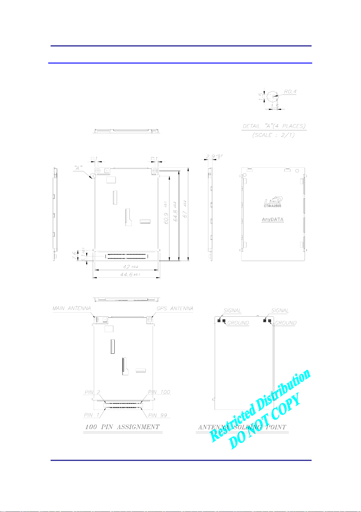
6. Mechanical Dimensions
6.1 DTEV-Dual Outline
TM
All Rights Reserved.
AD-2001-06-28 Ver 1.1
-40-
Page 41
AnyDATA.NET Inc. AnyTime AnyPlace Any Wireless Data Solution
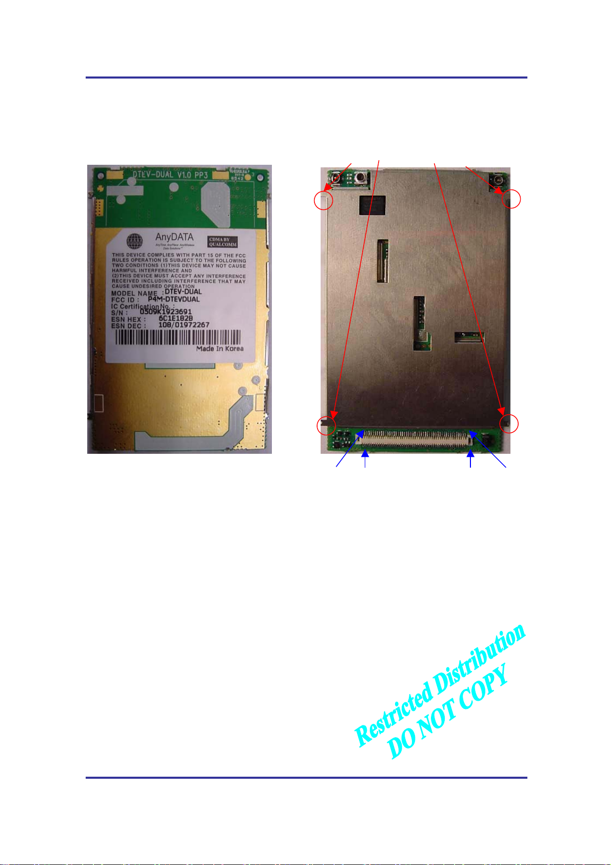
4 solder points in red circles MUST be soldered to PCB
GND in the host device
TM
PIN 2 PIN 1
PIN 99 PIN 100
Figure 6-1 DTEV-Dual Outline
All Rights Reserved.
AD-2001-06-28 Ver 1.1
-41-
Page 42
AnyDATA.NET Inc. AnyTime AnyPlace Any Wireless Data Solution
TM
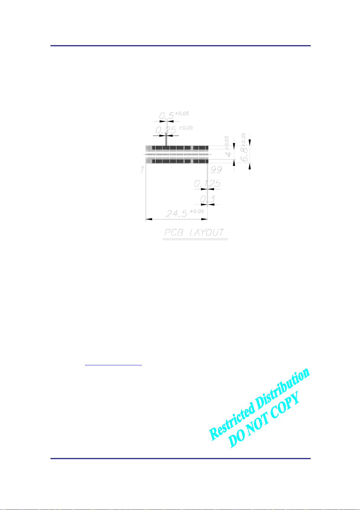
6.2 100-Pin Connector Mechanical Dimension
Figure 6-2 100-pin Connector
Counter-Part (the 100-pins socket connector (not in DTEV-Dual)):
Part Name: Socket pin connector (0.5mm pitch, straight, dual row)
Part Number: AXK5F00545J
Manufacture : NAIS
Note: For more information on the 100-pins socket connector,
Please visit http://www.nais-e.com/
P5 SERIES P5KF”
, click connector, and “NARROW PITCH(0.5mm) CONNECTORS
All Rights Reserved.
AD-2001-06-28 Ver 1.1
-42-
Page 43
AnyDATA.NET Inc. AnyTime AnyPlace Any Wireless Data Solution
.
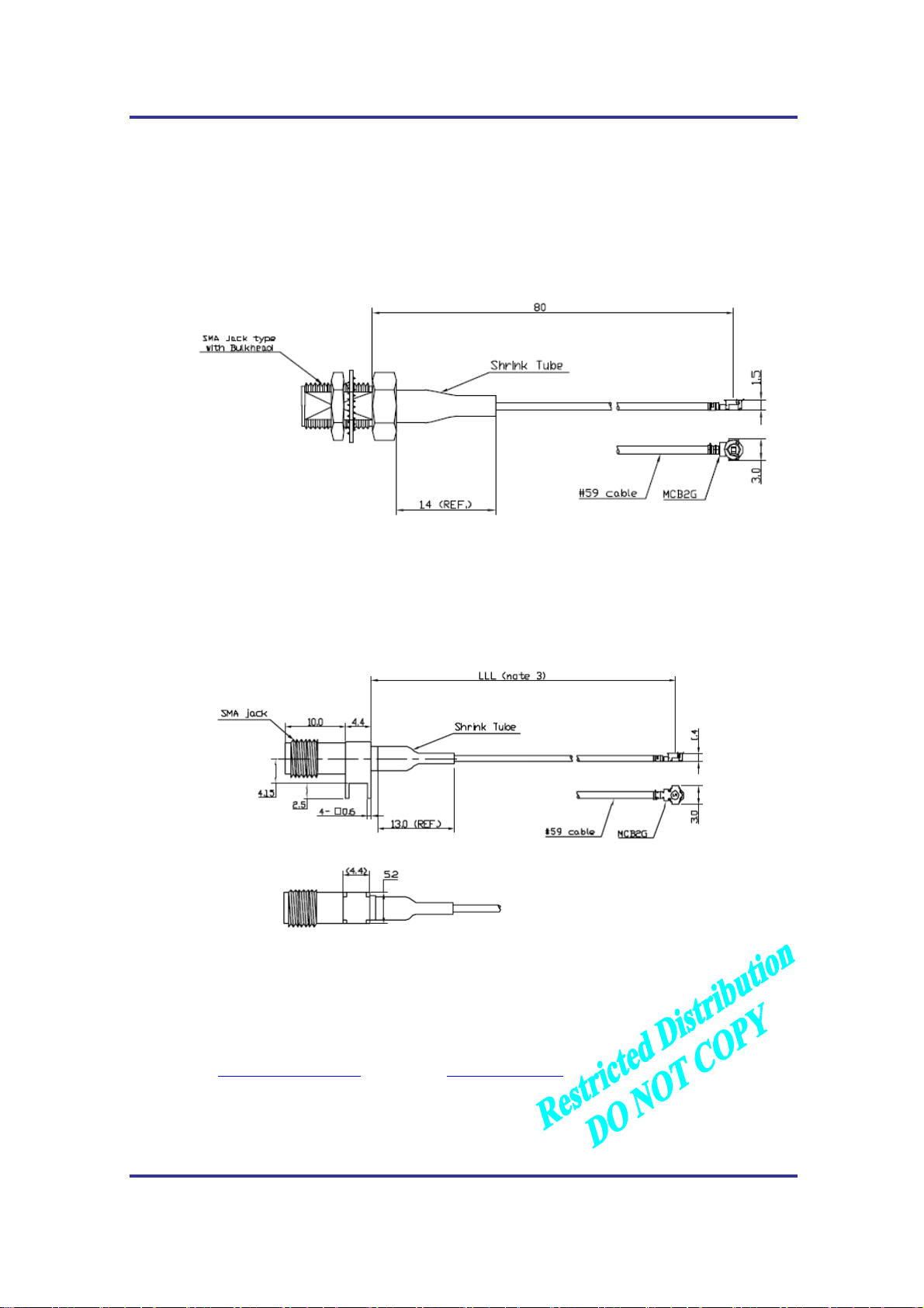
6.3 RF Connector
6.3.1 Cable Assembly, Sunridge Corp. Part
6.3.1.1 Bulkhead SMA Type cable : MCB2G-RH-59-LLL-SMAJB101
(Example, MCB2-RH-59-080-SMAJB101, 80mm-long RF cable)
Figure 6-3.1.1 Bulkhead SMA Type cable
TM
6.3.1.2 PCB mountable right angle SMA cable : MCB2G-RH-59-LLL-SMAJX103
(Example, MCB2G-RH-59-100-SMAJX103, 100mm-long RF cable)
Figure 6-3.1.2 PCB mountable right angle SMA cable
6.3.1.3 Contact Info.
Chris Su Tony Su
Tel: 626-535-1780 (CA, U.S.A.)
Fax : 626-535-1788 (CA, U.S.A.)
All Rights Reserved.
AD-2001-06-28 Ver 1.1
-43-
Page 44
AnyDATA.NET Inc. AnyTime AnyPlace Any Wireless Data Solution
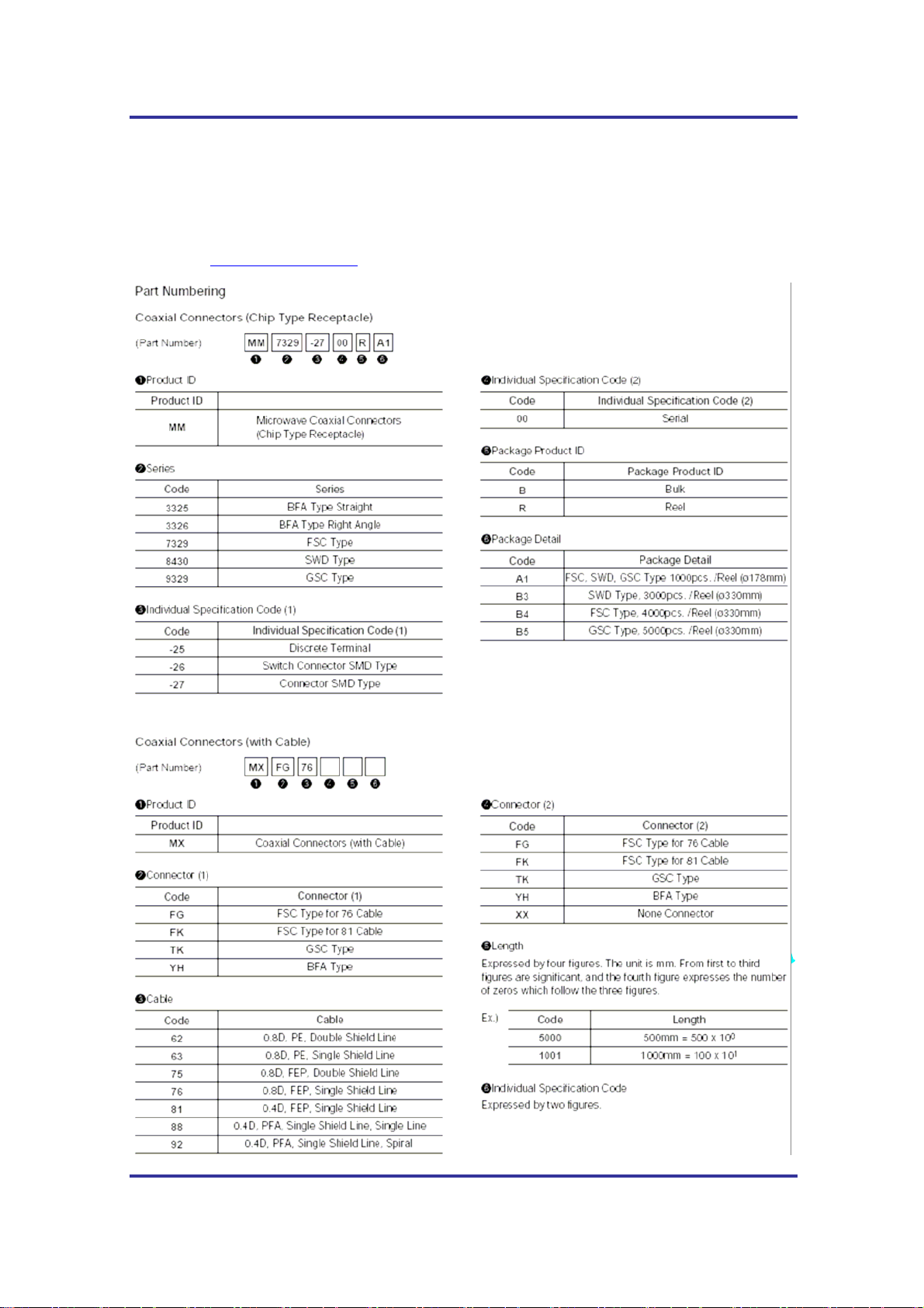
6.3.2 Murata Part
Our part number : MM9329-2700.
Counter part number : MXTK92( )( )( )
TM
Please, visit http://www.murata.com
and search for MXTK92 in product search engine
All Rights Reserved.
AD-2001-06-28 Ver 1.1
-44-
Page 45

AnyDATA.NET Inc. AnyTime AnyPlace Any Wireless Data Solution
7. Application Schematic
TM
Figure 7 Application Schematic
All Rights Reserved.
AD-2001-06-28 Ver 1.1
-45-
Page 46

AnyDATA.NET Inc. AnyTime AnyPlace Any Wireless Data Solution
8. Module Picture
TM
Figure 8 Module Picture
All Rights Reserved.
AD-2001-06-28 Ver 1.1
-46-
 Loading...