

Page 1

CDMA DATA TERMINAL
DT2000-Dual Reference Manual
Application Information
AnyDATA.NET
International Contact
United Computer &
Telecommunication Inc.
18902 Bardeen Ave
Irvine, CA 92612-1522, U.S.A.
October 2, 2002
01-DT2000-Dual-1 X3
AnyTime AnyPlace Any Wireless Data Solutions™
Korea Contact
AnyDATA.NET
Hanvit Bank Bldg. 6th Fl., 1-12
Byulyang-dong Kwachon,
Kyunggi-do, Korea
e-mail : [email protected]
e-mail : [email protected]
Page 2

AnyDATA.NET Inc. AnyTime AnyPlace Any Wireless Data Solution
TM
Notice
All data and information contained in or disclosed by this document are confidential and proprietary
information of AnyDATA.NET Inc., and all rights therein are expressly reserved. By accepting this
material, the recipient agrees that this material and the information contained therein are held in
confidence and in trust and will not be used, copied, reproduced, or distributed in whole or in part, nor its
contents revealed in any manner to others without the express written permission of AnyDATA.NET Inc.
AnyDATA.NET Inc. does not assume any liability arising out of the application or use of its products.
AnyDATA.NET Inc. assumes no responsibility for any damage or loss resulting from the misuse of its
products. AnyDATA.NET Inc. assumes no responsibility for any loss or claims by third parties, which
may arise through the use of its products. AnyDATA.NET Inc. assumes no responsibility for any damage
or loss caused by the deletion or loss of data as a result of malfunctions or repairs.
The information contained in this document is subject to change without notice. Information contained
herein is for reference only and does not constitute a commitment on the part of AnyDATA.NET Inc.
Although the information in this document has been carefully reviewed and it’s believed to be reliable,
AnyDATA.NET Inc. assumes no responsibility or liability for any errors or inaccuracies that may appear
in this document nor are they in anyway responsible for any loss or damage resulting from the use (or
misuse) of this document.
Warning: Exposure to Radio Frequency Radiation
!
The radiated output power of this device is far below the FCC radio frequency exposure limits.
Nevertheless, the device should be used in such a manner that the potential for human contact
during normal operation is minimized. In order to avoid the possibility of exceeding the FCC
radio frequency exposure limits, human proximity to the antenna should not be less than 20cm
during normal operation and the gain of the antenna must not exceed 1.5dBi.
All Rights Reserved.
AD-2001-06-28 Ver 1.1
-2-
Page 3

AnyDATA.NET Inc. AnyTime AnyPlace Any Wireless Data Solution
Contents
1 Introduction
1.1 Purpose
1.2 Organization
1.3 Revision History
1.4 Reference
1.5 Acronym List
2 Overview
2.1 Application Description
2.2 Technical Specifications
TM
2.2.1 General Specification
2.2.2 Receive Specification
2.2.3 Transmit Specification
2.2.4 Standards
2.3 Interface Diagram
2.4 General Features
3 PIN Description
3.1 I/O Description Parameters
3.2 PIN Names and Pinouts
3.2.1 60-PIN Connector
3.3 60-Pin Connector Pinout (Top view)
4 Interface Descriptions
4.1 Overview
4.2 CODEC Interface
4.3 UART Interface
All Rights Reserved.
AD-2001-06-28 Ver 1.1
-3-
Page 4

AnyDATA.NET Inc. AnyTime AnyPlace Any Wireless Data Solution
4.3.1 Primary UART Interface
4.3.2 Secondary UART Interface
4.4 General Purpose Interface
4.5 External Hardware Reset
4.6 LEDs
4.7 User Interface
4.7.1 Key Pad
4.7.2 LCD
4.7.3 Ringer
5 Electrical Specifications
5.1 DC Electrical Specifications
5.1.1 Absolute Maximum Ratings
TM
5.1.2 Recommended Operating Conditions
5.1.3 Power Consumption
5.1.4 Serial Interface Electrical Specifications
5.2 Timing Characteristics
5.2.1 External CODEC Timing
5.2.2 LCD Timing
6 Mechanical Dimension
6.1 DT2000-Dual Outline
6.2 60-Pin Connector
6.3 RF Connector
All Rights Reserved.
AD-2001-06-28 Ver 1.1
-4-
Page 5

AnyDATA.NET Inc. AnyTime AnyPlace Any Wireless Data Solution
Figures
Figure 2-1 Interface Block Diagram ....................................................................................... 11
Figure 2-2 General Features ................................................................................................... 12
Figure 4-1 Interface Block Diagram ....................................................................................... 16
Figure 4-2 Keypad Matrix ...................................................................................................... 21
Figure 4-3 LCD Interface Block Diagram .............................................................................. 22
Figure 4-4 Reference External Ringer Driver Circuit ............................................................. 23
Figure 5-1 External PCM CODEC to Module timing ............................................................ 25
Figure 5-2 Module to External PCM CODEC timing ............................................................ 25
Figure 5-3 LCD Timing .......................................................................................................... 26
Figure 6-1 60-pin Female Connector …………………………………………………………... 29
Figure 6-2 PCB Connector .……………………………………………………………………..30
Figure 6-3 PCB Connector Layout .……………………………………………………………. 30
TM
Figure 6-4 Mechanical Characteristics of Cable Harness Assembly .……………………….…. 31
All Rights Reserved.
AD-2001-06-28 Ver 1.1
-5-
Page 6

AnyDATA.NET Inc. AnyTime AnyPlace Any Wireless Data Solution
Table s
Table 1-1 Revision History ....................................................................................................... 7
Table 3-1 60-PIN Connector Pinouts ..................................................................................... 15
Table 4-1 Analog Audio Pinouts ............................................................................................ 17
Table 4-2 Digital CODEC Pinouts ......................................................................................... 18
Table 4-3 UART Interface Pinouts ......................................................................................... 18
Table 4-4 Secondary UART Interface Pinouts ………………………………………………… 19
Table 4-5 General Purpose Interface Pinouts ......................................................................... 19
Table 4-6 LED Pinouts ………………………………………………………………………… 20
Table 4-7 LCD Interface Signals ............................................................................................ 22
Table 5-1 Absolute Maximum Ratings ................................................................................... 24
Table 5-2 External PCM CODEC Parameters ........................................................................ 26
Table 5-3 LCD Timing Parameters .......................................................................................... 27
TM
All Rights Reserved.
AD-2001-06-28 Ver 1.1
-6-
Page 7
AnyDATA.NET Inc. AnyTime AnyPlace Any Wireless Data Solution
1. Introduction
1.1 Purpose
This Manual provides hardware interface and programming information for the DT2000-Dual
CDMA Wireless Data Module.
1.2 Organization
This Manual will discuss the interface and operation of the module and is divided into the following
subsections:
Section 2 – Introduces users to the DT2000-Dual CDMA Wireless Data Module’s basic features
and general specifications.
Section 3 – Lists each DT2000-Dual pin and its function within the device. The pinout for the
TM
module is listed in numeric sequence.
Section 4 – Specifies the recommended operating conditions, DC voltage characteristics, I/O
timing, and power estimations for the module. Timing diagrams are also included.
Section 5 – Details each subsystem or block within the module and shows how the subsystem
or block interfaces with external peripherals.
Section 6 – Provides package dimensions for the module.
1.3 Revision History
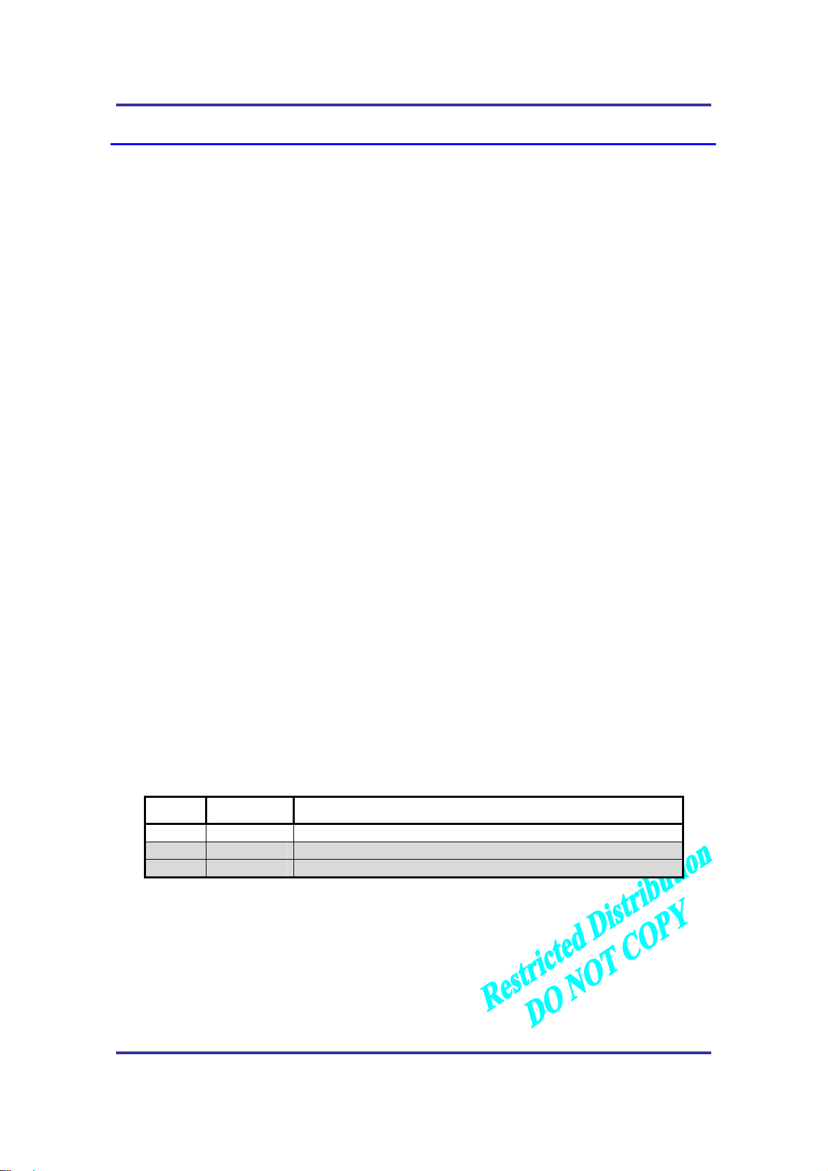
The revision history for this document is shown in Table 1-1.
Table 1-1 Revision History
Version Date Description
V1_X1 April 2001 Initial Release – applicable DTS and DTSS series software
V1_X2 June 2001 Corrected document format
V1_X3 Oct. 2002 Corrected document content
1.4 References
All Rights Reserved.
AD-2001-06-28 Ver 1.1
-7-
Page 8

AnyDATA.NET Inc. AnyTime AnyPlace Any Wireless Data Solution
1. QUALCOMM Incorporated. MSM5100 Mobile Station Modem: Component Supply
Specification. 80-V2180-7-X1, July 13, 2001.
2. QUALCOMM Incorporated. MSM5100 Mobile Station Modem: Device Specification
(Preliminary Information). 93-V2180-1-X3, August 30, 2001.
3. QUALCOMM Incorporated. SURF5100 User Manual. 80-V2535-1-X1, March 28, 2001.
1.5 Acronym List
Term Definition
CDMA Code-Division Multiple Access
CODEC Coder-Decoder
GPIO General-purpose Input/Output
JTAG Joint Test Action Group (ANSI/ICEEE Std. 1149.1-1990)
LCD Liquid Crystal Display
LDO Voltage Regulator
LED Light Emitting Diode
PCB Printed Circuit Board
PCM Pulse Coded Modulation
PCS Personal Communications Service
RF Radio Frequency
Rx Receive
TCXO Temperature-Controlled Crystal Oscillator
Tx Transmit
UART Universal Asynchronous Receiver Transmitter
TM
All Rights Reserved.
AD-2001-06-28 Ver 1.1
-8-
Page 9

AnyDATA.NET Inc. AnyTime AnyPlace Any Wireless Data Solution
TM
2. Overview
2.1 Application Descriptions
The CDMA Wireless Data Module is a complex consumer communications instrument that relies
heavily on both digital signal and embedded processor technologies. The Wireless Data Modules
manufactured by AnyDATA.NET support Code-Division Multiple Access (CDMA). This operates in
both the cellular and PCS spectrum.
In a continuing effort to simplify the design and to reduce the production cost of the Wireless Data
Module, AnyDATA.NET has successfully developed the DT2000 series. The DT2000-Dual is
AnyDATA.NET’s latest compact Wireless Data Module operating in the Cellular and PCS spectrum. The
DT2000-Dual also contains a complete digital modulation and demodulation system for CDMA standards
as specified in IS-95 A/B and IS-2000.
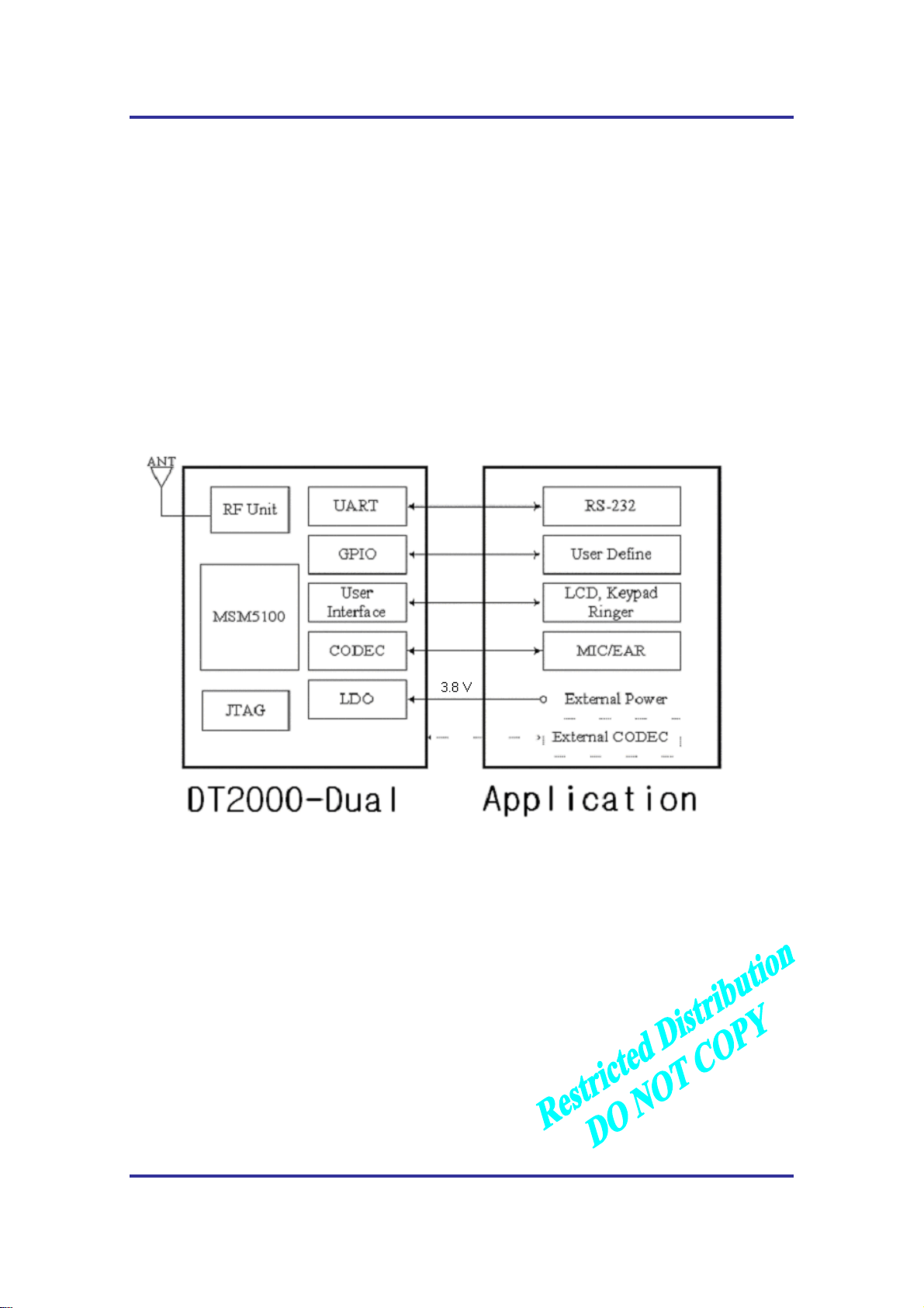
The subsystem in the DT2000-Dual includes a CDMA processor (MSM5100), an integrated
CODEC with an ear piece and microphone amplifiers, and an RS-232 serial interface supporting forward
link data communications at a rate of 230.4kbps.
The DT2000-Dual provides an external interface that includes the standard RS-232, Digital Audio,
External reset control, LCD Display, Keypad, and Ringer extension ports.
The DT2000-Dual has the capability to power down unused circuits in order to dynamically
minimize power consumption.
All Rights Reserved.
AD-2001-06-28 Ver 1.1
-9-
Page 10
AnyDATA.NET Inc. AnyTime AnyPlace Any Wireless Data Solution
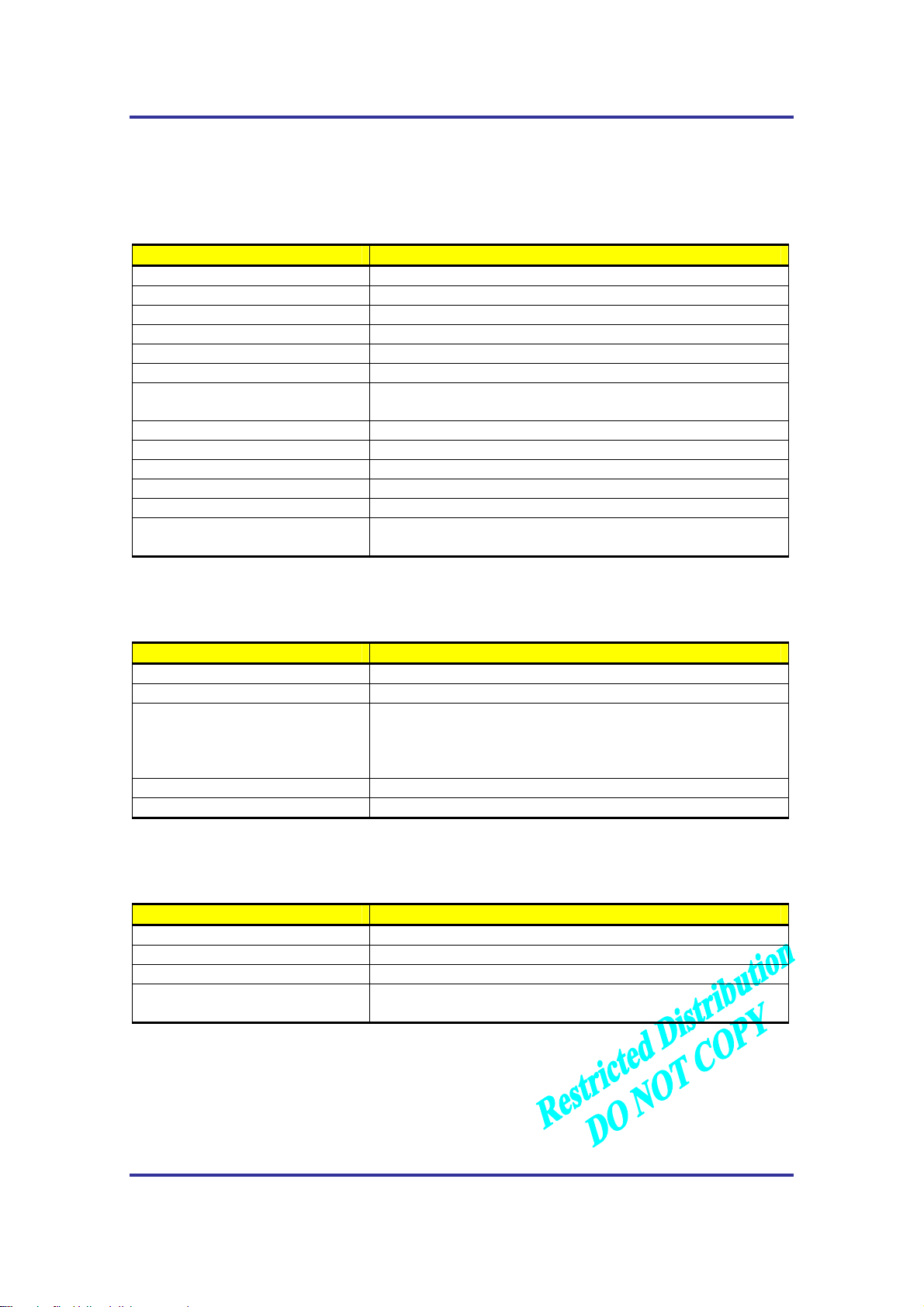
2.2 Technical Specifications
2.2.1 General Specifications
Parameters Descriptions
External Access Code-Division-Multiple-Access (CDMA)
CDMA Protocol IS-95 A/B, IS-98A, IS-126, IS-637A, IS-707A, IS-2000
Data Rate 153.6Kbps max
Transmit/Receive Frequency Interval 45MHz for Cellular and 80MHz for PCS
Number of Channel 832 for Cellular and 42 for PCS
Operating Voltage DC +3.4V ~ +4.2V
Current Consumption Stand by mode: Idle (110mA), Sleep (2mA)
Busy mode: 900mA (Max)
Operating Temperature -30ºC ~ +60ºC
Frequency Stability ±300Hz for Cellular and ±150Hz for PCS
Antenna MCA Connector, 50ohm
Size 39 X 49 X 6.0mm with case
Weight About 20g
External Interface RS-232, Digital/Analog Audio, LCD, Keypad, Ringer
External Reset Control
TM
2.2.2 Receive Specifications
Parameters Descriptions
Frequency Range 869.04 ~ 893.97 MHz for Cellular and 1931.25 ~ 1988.75MHz for PCS
Sensitivity Below –104 dBm
Interference Rejection Single tone (-30dBm @900KHz): Below –101dBm
Two tone (-43 dBm @900KHz and 1700KHz): Below –101dBm
Two tone (-32 dBm @900KHz and 1700KHz): Below –90dBm
Two tone (-21 dBm @900KHz and 1700KHz): Below –79dBm
Spurious Wave Suppression Below –80dBc
Input Dynamic Range -25 dBm ~ -104dBm
2.2.3 Transmit Specifications
Parameters Descriptions
Frequency Range
Nominal Power 0.32 W (24.7dBm)
Minimum Controlled Output Power Below –50dBm
Max Power Spurious 900KHz: Below –42dBc/30KHz
824.04 ~ 848.97 MHz for Cellular and 1851.25 ~ 1908.75MHz for PCS
1.98MHz: Below –54dBc/30KHz
All Rights Reserved.
AD-2001-06-28 Ver 1.1
-10-
Page 11
AnyDATA.NET Inc. AnyTime AnyPlace Any Wireless Data Solution
2.2.4 Standards
IS-95 A/B: Protocol Between MS & BTS
IS-96A: Voice Signal Coding
IS-98A: Base MS Function
IS-126: Voice Loop-Back
IS-637: Short Message Service
IS-707: Data Service
2.3 Interface Diagram
TM
Figure 2-1 Interface Block Diagram
All Rights Reserved.
AD-2001-06-28 Ver 1.1
-11-
Page 12
AnyDATA.NET Inc. AnyTime AnyPlace Any Wireless Data Solution
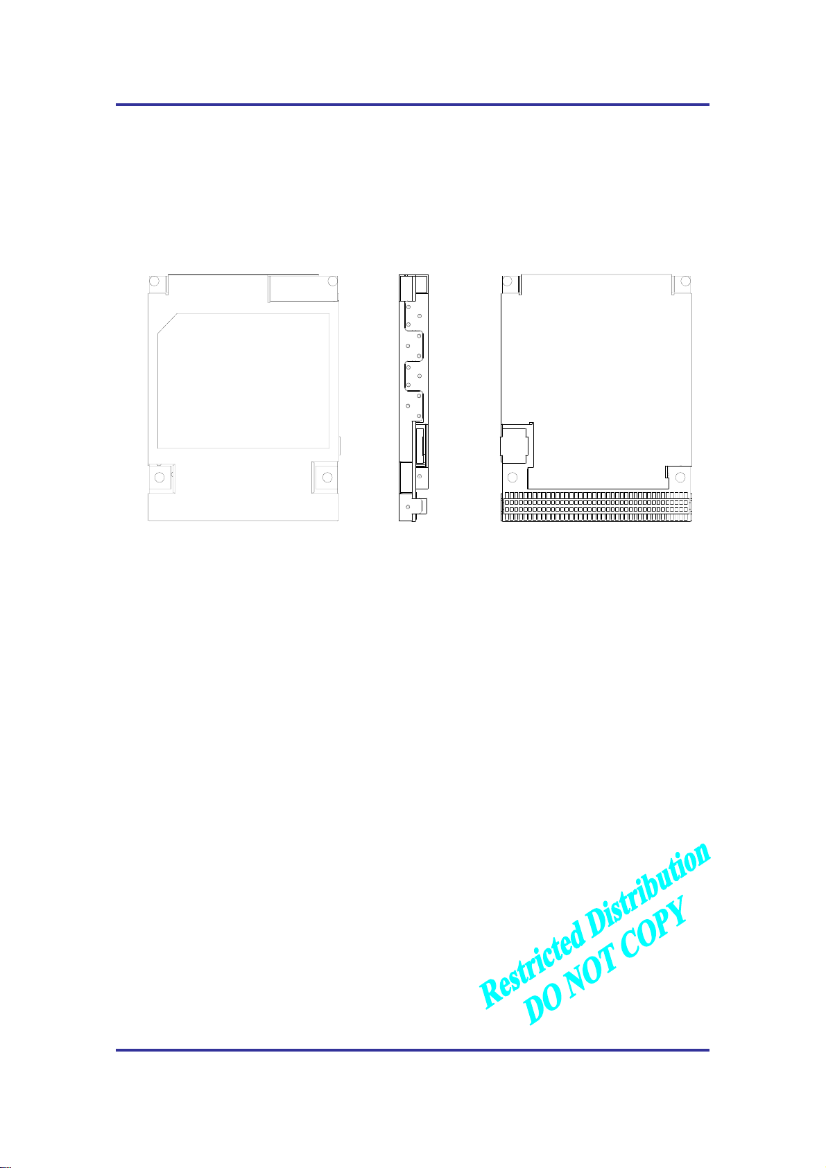
2.4 General Features
TM
Figure 2-2 General Features
All Rights Reserved.
AD-2001-06-28 Ver 1.1
-12-
Page 13

AnyDATA.NET Inc. AnyTime AnyPlace Any Wireless Data Solution
3. PIN Description
3.1 I/O Description Parameters
Symbol Description
I
O Output
B Bi-directional
N Voltage or Current Level
IS Input with Schmitt Trigger
BS Bi-directional Schmitt Trigger
PU Internal Pull-Up
PD Internal Pull-Down
KP Internal Weak Keeper Device (Keepers cannot drive external buses.)
3.2 PIN Names and Pinouts
CMOS Input
TM
3.2.1 60-Pin Connector
PIN NAME TYPE DESCRIPTION
1
2 MSM_DP_RI/ (GPIO_INT25) BS-PD Ring indicator
3 MSM_DP_RFR/ O Ready for receive
4 MSM_DP_TXD O Transmit data
5 MSM_DP_DTR/ (GPIO_INT2) BS-PU Data terminal ready
6 MSM_DP_RXD IS-PD Receive data
7 MSM_DP_CTS/ IS-PD Clear to send
8 GND GND Signal ground
9 AUX_PCM_DIN IS-PD External CODEC PCM data input, RXD *
10 GND GND Signal ground *
11 AUX_PCM_DOUT BS_PU External CODEC PCM data output, TXD *
12 GPIO_INT22 (PRE_DIAL) BS_PU General purpose input output
13 AUX_PCM_CLK BS_PD External CODEC PCM clock
14 AUX_PCM_SYNC BS_PD External CODEC PCM sync.
15 GPIO_INT23 (SMS_LED) BS_PU General purpose input output
16 GPIO_INT03 (IDLE_LED) BS_PU General purpose input output
17 GPIO_INT04 (BUSY_LED) BS_PU General purpose input output
18 EXT_RESET I External Hardware Reset
19 GPIO_INT09 (HOST_RESET) BS_PD General purpose input output
20 GPIO_INT12 BS_PU General purpose input output
21 GPIO_INT13 BS_PD General purpose input output
22 GPIO_INT17 (PS_HOLD) BS_PD General purpose input output
23 RINGER O Ringer output
24 D00 B-KP Data line
25 D01 B-KP Data line
All Rights Reserved.
MSM_DP_DCD/ (GPIO_INT16)
BS-PD Data carrier detect
AD-2001-06-28 Ver 1.1
-13-
Page 14

AnyDATA.NET Inc. AnyTime AnyPlace Any Wireless Data Solution
PIN NAME TYPE DESCRIPTION
26 D02 B-KP Data line
27 D03 B-KP Data line
28 D04 B-KP Data line
29 D05 B-KP Data line
30 D06 B-KP Data line
31 D07 B-KP Data line
32 A01 B Address line
33 RES_OUT/ B Reset output
34 LCD_CS/ (GPIO_INT40) BS-PU LCD chip select
35 RD/ B Read enable output
36 LWR/ BS-PU Write enable output
37 BATT+ I Battery Monitoring **
38 GND GND Signal ground
39 VEXT_DC I External power input
40 VEXT_DC I External power input
41 MIC1P
42 MIC1N
43 EAR1P O Balanced Analog Audio Output (Speaker)
44 EAR1N O Balanced Analog Audio Output (Speaker)
45 GPIO_INT33 (KEYPAD_15) BS_PU General purpose input output
46 GPIO_INT35 (KEYPAD_11) BS_PU General purpose input output
47 GPIO_INT14 (MOTOR) BS_PD General purpose input output
48 GPIO_INT36 (KEYPAD_9) BS_PU General purpose input output
49 GPIO_INT34 (KEYPAD_13) BS_PU General purpose input output
50 KEYSENSE4/ (ON_SW) IS_PU Key sense input
51 KEYSENSE1/ IS_PU Key sense input
52 KEYSENSE2/ IS_PU Key sense input
53 KEYSENSE3/ IS_PU Key sense input
54 KEYSENSE0/ IS_PU Key sense input
55 LCD_E (GPIO_INT41) BS-PD LCD read enable
56 A00 B Address line
57 EAR_DET1 I Ear Kit Detect (small headset)
58 MIC2 (MIC) I Analog Audio Input (MIC) (small headset)
59 GND (GND_A) GND Signal ground (small headset)
60 EAR_JACK+ (EAR)
I
I
O
Notes:
Balanced Analog Audio Input (MIC)
(Speaker)
Balanced Analog Audio Input (MIC)
(Speaker)
Analog Audio Output (Speaker) (small
headset)
TM
* If not used as PCM, it can be used as a secondary UART for debugging. We strongly recommend that
the user has a 3-pin connector or 3 test points on their board, so that one can easily monitor and diagnose
their module.
** If the user wants the module to monitor battery voltage and the user is using a regulator in conjunction
with a battery, whose maximum voltage exceeds 4.3 V, to drive the module, then the user should please
contact our engineers.
When using a battery in which the voltage is between 3.3 V to 4.3 V and regulators aren’t used to drive
the module, leave this pin open.
All Rights Reserved.
AD-2001-06-28 Ver 1.1
-14-
Page 15

AnyDATA.NET Inc. AnyTime AnyPlace Any Wireless Data Solution
3.3 60-PIN Connect Pinouts (Topview)
Table 3-1 60-PIN Connector Pinouts
TM
1 MSM_DP_DCD/
3 MSM_DP_RFR/
5 MSM_DP_DTR/
7 MSM_DP_CTS/
9 AUX_PCM_DIN
11 AUX_PCM_DOUT
13 AUX_PCM_CLK
15 GPIO_INT23
17 GPIO_INT04
19 GPIO_INT09
21 GPIO_INT13
23 RINGER
25 D01
27 D03
29 D05
31 D07
33 RES_OUT/
35 RD/
37 BATT+
39 VEXT_DC
41 MIC1P
43 EAR1P
45 GPIO_INT33
47 GPIO_INT14
49 GPIO_INT34
51 KEYSENSE1/
53 KEYSENSE3/
55 LCD_E
57 EAR_DET1
59 GND
2 MSM_DP_RI/
4 MSM_DP_TXD
6 MSM_DP_RXD
8 GND
10 GND
12 GPIO_INT22
14 AUX_PCM_SYNC
16 GPIO_INT03
18 EXT_RESET
20 GPIO_INT12
22 GPIO_INT17
24 D00
26 D02
28 D04
30 D06
32 A01
34 LCD_CS/
36 LWR/
38 GND
40 VEXT_DC
42 MIC1N
44 EAR1N
46 GPIO_INT35
48 GPIO_INT36
50 KEYSENSE4/
52 KEYSENSE2/
54 KEYSENSE0/
56 A00
58 MIC2
60 EAR_JACK+
All Rights Reserved.
AD-2001-06-28 Ver 1.1
-15-
Page 16
AnyDATA.NET Inc. AnyTime AnyPlace Any Wireless Data Solution
TM
4. Interface Descriptions
4.1 Overview
This chapter covers information required to convert the DT2000-Dual into a subscriber unit
application. In addition, some of the internal blocks of the device are described. Understanding these
internal blocks is necessary for one to completely grasp the functions of the various interfaces.
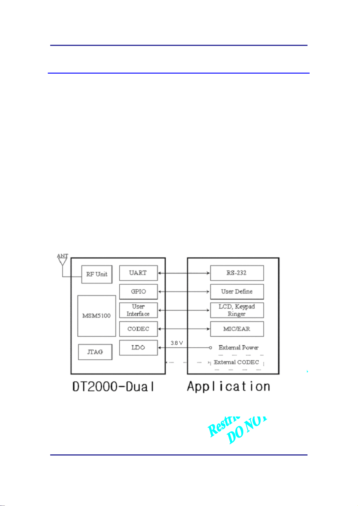
This chapter discusses the interface to the major blocks of the DT2000-Dual as shown in the
following figure. These blocks include:
CODEC Interface
UART Interface
General Purpose Interface
User Interface
JTAG Interface
Figure 4-1 Interface Block Diagram
All Rights Reserved.
AD-2001-06-28 Ver 1.1
-16-
Page 17
AnyDATA.NET Inc. AnyTime AnyPlace Any Wireless Data Solution
TM
4.2 CODEC Interface
The CODEC Interface is configured by internal and external figures. If the internal CODEC
interface is used, additional glue logic is not necessary and the module’s very simple audio interface can
be used. Otherwise if the internal CODEC interface is not used, an external CODEC is necessary to
support the car-kit system. In this case, the module provides a PCM CODEC Interface.
4.2.1 Internal CODEC Interface
The module contains analog audio interface circuitry. The contained audio interface supports all of the
required conversation and amplification stages for the audio front end.
The audio interface includes the amplification stages for both the microphone and earphone. The
interface supports one single-ended microphone input and one single-ended earphone output.
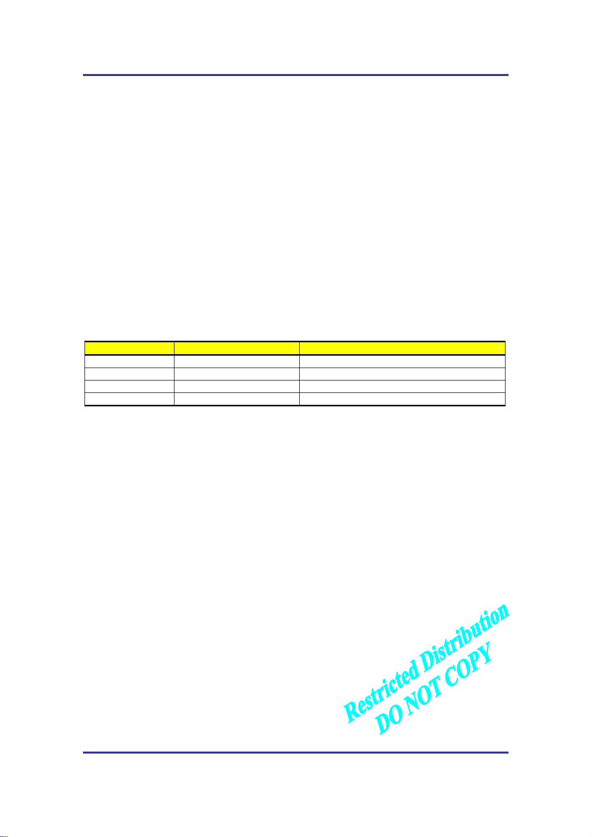
Table 4-1 Analog Audio Pinouts
NAME
MIC2
EAR_DET1 EAR/MIC Set Detect Logic Input (Pin No. 57) **
EAR_JACK+ Earphone Output Analog Output (Pin No. 60)
GND_A Audio Ground Audio Ground (Pin No. 59)
Note:
DESCRIPTION CHARACTERISTIC
MIC Input Analog Input (Pin No. 58) *
* MIC2, along with being a microphone input, checks to see if the user has pressed the headset key,
which allows the user to connect to or disconnect from a call. This pin is internally pulled high and is
therefore normally in the high state. To activate this input and connect to or disconnect from a call, the
user must set the MIC2 pin to a low state for 100ms to 200ms.
** EAR_DET1 checks to see if a headset has been connected to the ear-jack. When there is no headset
connected to the ear-jack, the audio path is disconnected. When a headset is connected to the ear-jack an
audio path is opened. To simulate a headset connected to the ear-jack, the user must apply a low signal to
the EAR_DET1 pin for as long as the user wants the audio path to be kept open.
All Rights Reserved.
AD-2001-06-28 Ver 1.1
-17-
Page 18
AnyDATA.NET Inc. AnyTime AnyPlace Any Wireless Data Solution
4.2.2 Extended CODEC Interface
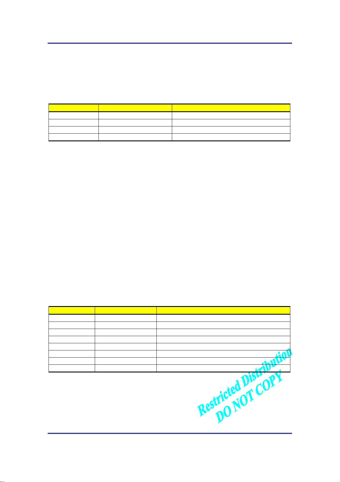
The PCM CODEC interface is used for the car-kit audio system. This interface is optional.
External CODEC interface signals are listed below:
Table 4-2 Digital CODEC Pinouts
NAME DESCRIPTION PINOUTS
AUX_PCM_CLK
AUX_PCM_DIN PCM Data Input Pin No. 9
AUX_PCM_DOUT PCM Data Output Pin No. 11
AUX_PCM_SYNC PCM Sync. Pin No. 14
PCM Clock Pin No. 13
4.3 UART Interface
4.3.1 Primary UART interface
The Universal Asynchronous Receiver Transmitter (UART) communicates with serial data that
TM
conforms to the RS-232 Interface protocol. The module provides 3.0V CMOS level outputs and 3.0V
CMOS switching input levels. In addition, all inputs have a 5.0V tolerance, however 3.0V or 3.3V CMOS
logic compatible signals are highly recommended.
All the control signals of the RS-232 are active low, however the data signals, RXD and TXD, are
active high.
The UART has a 64 byte transmit (TX) FIFO and a 64 byte receive (RX) FIFO. The UART features
hardware handshaking, programmable data sizes, programmable stop bits, and odd, even, no parity. The
UART operates at a maximum bit rate of 115.2kbps.
Table 4-3 UART Interface Pinouts
NAME
DP_DCD/
DP_RI/
DP_RFR/
DP_TXD
DP_DTR/
DP_RXD
DP_CTS/ Clear to Send Clear to send to the host
GND Signal Ground Signal ground
DESCRIPTION CHARACTERISTIC
Data Carrier Detect Network connected from the module
Ring Indicator Output to host indicating coming call
Ready for Receive Ready for receive from host
Transmit Data Output data from the module
Data Terminal Ready Host ready signal
Receive Data Input data to the module
Reference Plane: DT2000 Dual
All Rights Reserved.
AD-2001-06-28 Ver 1.1
-18-
Page 19
AnyDATA.NET Inc. AnyTime AnyPlace Any Wireless Data Solution
TM
4.3.2 Secondary UART interface
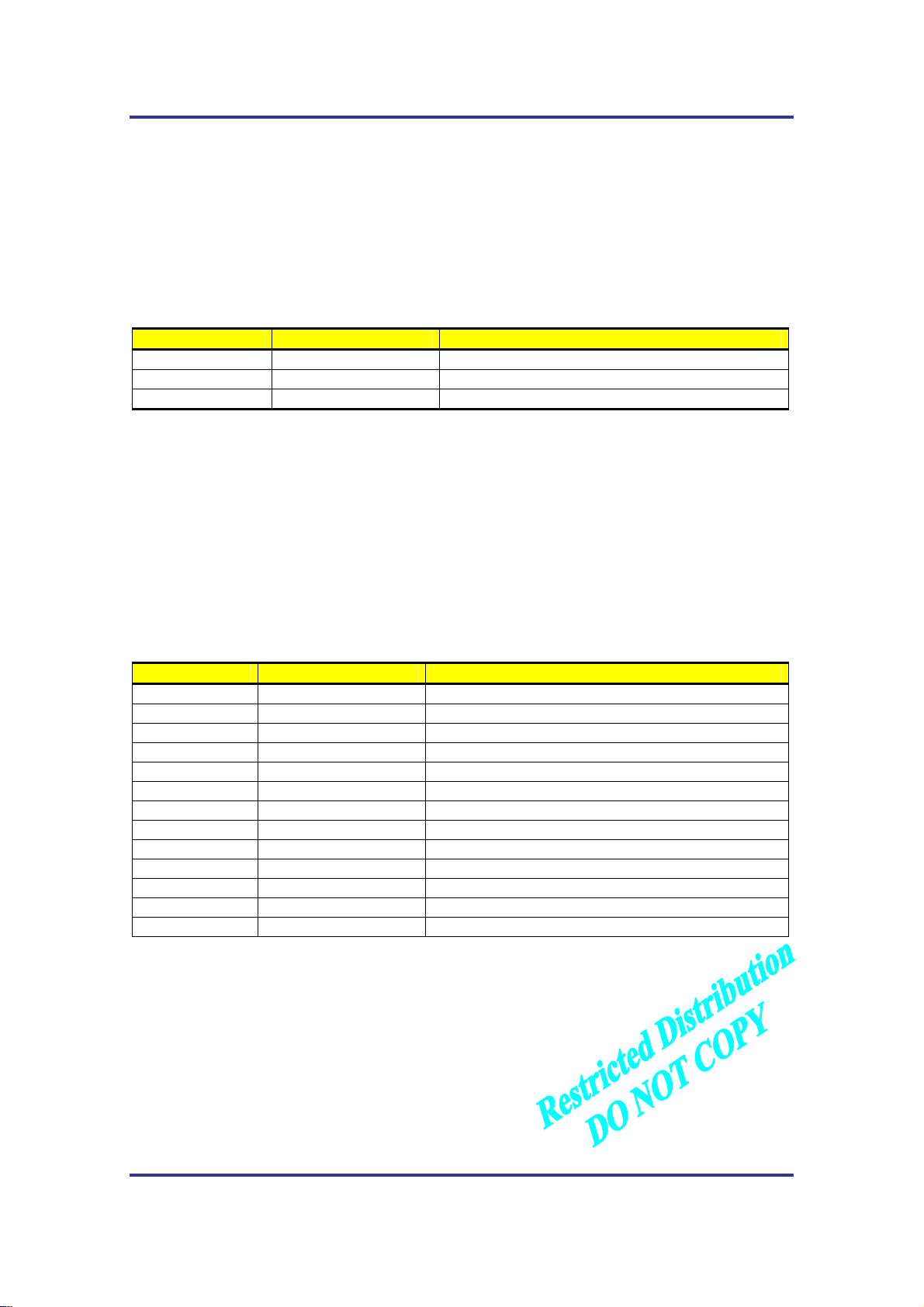
The secondary UART is used to monitor and diagnose the status of the DT2000-Dual. It is strongly
recommended for the user to have the following secondary UART pins connected to an extra connector or
to test points, in order to easily troubleshoot any problems with the module.
Table 4-4 Secondary UART Interface Pinouts
NAME
AUX_PCM_DIN/
AUX_PCM_DOUT/ Data Output Output data from the module
GND Signal Ground Signal ground
DESCRIPTION CHARACTERISTIC
Data Input Input data to the module
Reference Plane: DT2000 Dual
4.4 General Purpose Interface
The general purpose interface consists of 13 user-definable bi-directional pins.
Each GPIO pin can be configured as an input interrupt source. In addition, some GPIO pins can be
used as output control pins from the module. The user can define these pins properly as follows.
Table 4-5 General Purpose Interface Pinouts
NAME
GPIO_INT03 BS_PU Configured as a pull-up, Bi-directional
GPIO_INT04 BS_PU Configured as a pull-up, Bi-directional
GPIO_INT09 BS_PD Configured as a pull-down, Bi-directional
GPIO_INT12 BS_PU Configured as a pull-up, Bi-directional
GPIO_INT13 BS_PD Configured as a pull-down, Bi-directional
GPIO_INT14 BS_PD Configured as a pull-down, Bi-directional
GPIO_INT17 BS_PD Configured as a pull-down, Bi-directional
GPIO_INT22 BS_PU Configured as a pull-up, Bi-directional
GPIO_INT23 BS_PU Configured as a pull-up, Bi-directional
GPIO_INT33 BS_PU Configured as a pull-down, Bi-directional
GPIO_INT34 BS_PU Configured as a pull-down, Bi-directional
GPIO_INT35 BS_PU Configured as a pull-down, Bi-directional
GPIO_INT36 BS_PU Configured as a pull-down, Bi-directional
TYPE CHARACTERISTIC
4.5 External Hardware Reset
There are two types of resets that the user can employ to restart the module. The first type will reset
the MSM and the memory and is performed when the user gives the AT command, AT+RESET, to the
MSM. Another way to reset the module is by using the external hardware reset. This type of reset will
reset the hardware as well as the MSM and the memory. The flash memory will be the only information
that is kept. To perform an external hardware reset, make sure the module has powered on and is not in
All Rights Reserved.
AD-2001-06-28 Ver 1.1
-19-
Page 20
AnyDATA.NET Inc. AnyTime AnyPlace Any Wireless Data Solution
TM
the initialization stage, and then apply a high signal of 2.5 V to 3.7 V to the external hardware reset pin
for 200ms to 500ms. Keep the external hardware reset pin low when the module is initializing as well as
during normal operation.
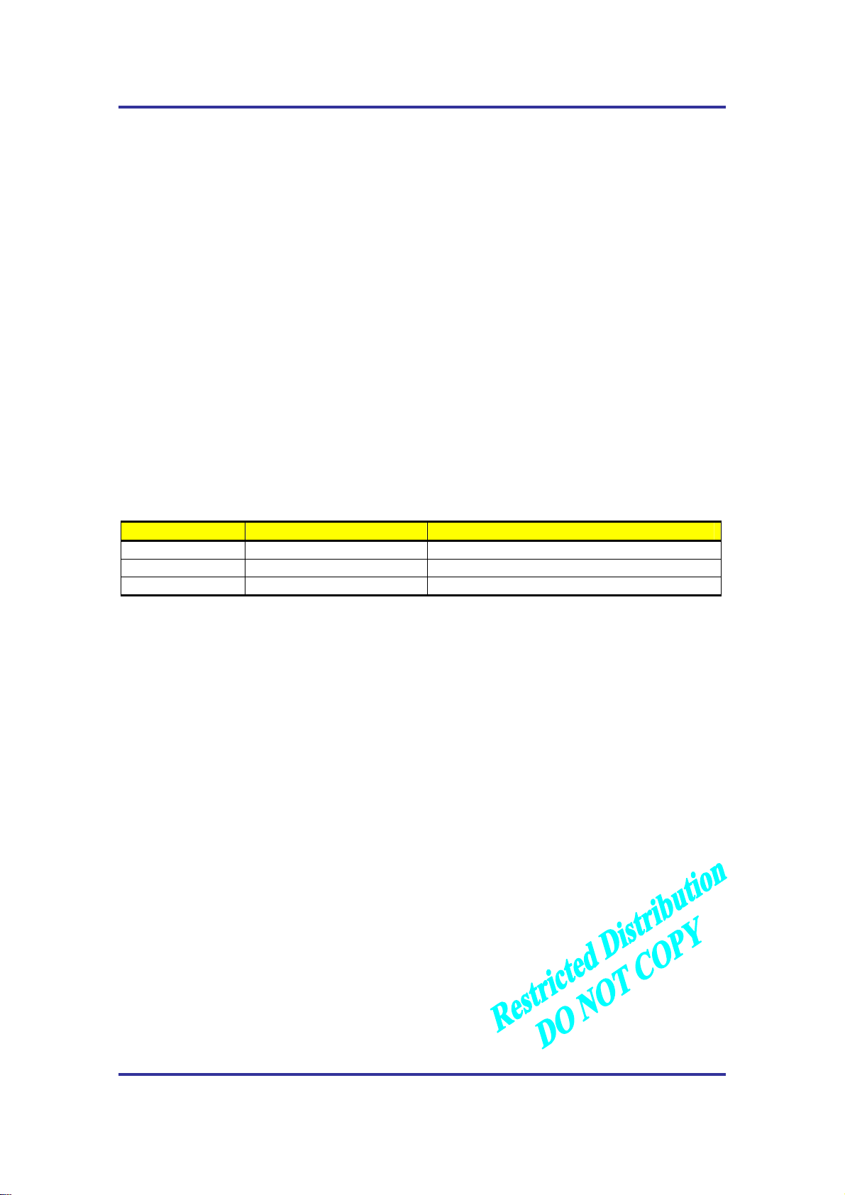
4.6 LEDs
The DT2000-Dual can indicate its current status through three pins. These three pins can be
connected to LEDs to more quickly and easily determine the status of the module. The SMS LED
indicates to the user if there is a SMS message or a voicemail message. If there is a SMS message or a
voicemail message, the SMS LED will turn on. After the user has read the SMS message or listened to the
voicemail message, the SMS LED turns off. Shortly after the module has been turned on, the Idle LED
should turn on indicating that the module is in-service. This means that the module is within the range of
the base station and is able to receive a signal from the base station. When the module is in traffic or
conversation stage, the Busy LED is on.
Table 4-6 LED Pinouts
NAME DESCRIPTION PINOUTS
GPIO_INT23 SMS_LED Pin No. 15
GPIO_INT03 IDLE_LED Pin No. 16
GPIO_INT04 BUSY_LED Pin No. 17
All Rights Reserved.
AD-2001-06-28 Ver 1.1
-20-
Page 21
AnyDATA.NET Inc. AnyTime AnyPlace Any Wireless Data Solution
4.7 User Interface
4.7.1 Keypad
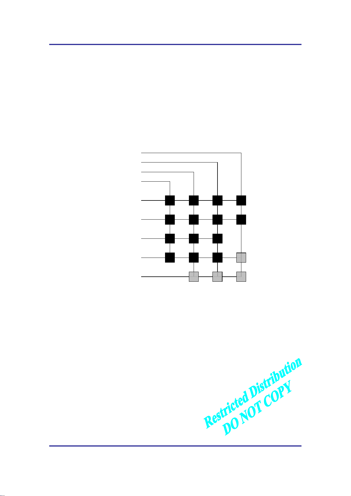
The keypad interface consists of a 4 X 5 matrix pattern. Only 4 of the 5-KEYSENSE/[4:0] pins are
used to connect a matrix keypad to the module. The KEYSENSE/ pins are active low.
5-GPIO pins are necessary to construct the other side of the matrix. These 5-GPIO pins must be active
high in order for the keypad matrix to work properly. The general keypad matrix is shown below:
KEYSENSE0/
KEYSENSE1/
KEYSENSE2/
KEYSENSE3/
TM
1-GPIO
2-GPIO
3-GPIO
4-GPIO
#
9
6
3
0
8
5
2
*
7
4
1
SEND
END
5-GPIO
Reserved
Figure 4-2 Keypad Matrix
All Rights Reserved.
AD-2001-06-28 Ver 1.1
-21-
Page 22
AnyDATA.NET Inc. AnyTime AnyPlace Any Wireless Data Solution
TM
4.7.2 LCD
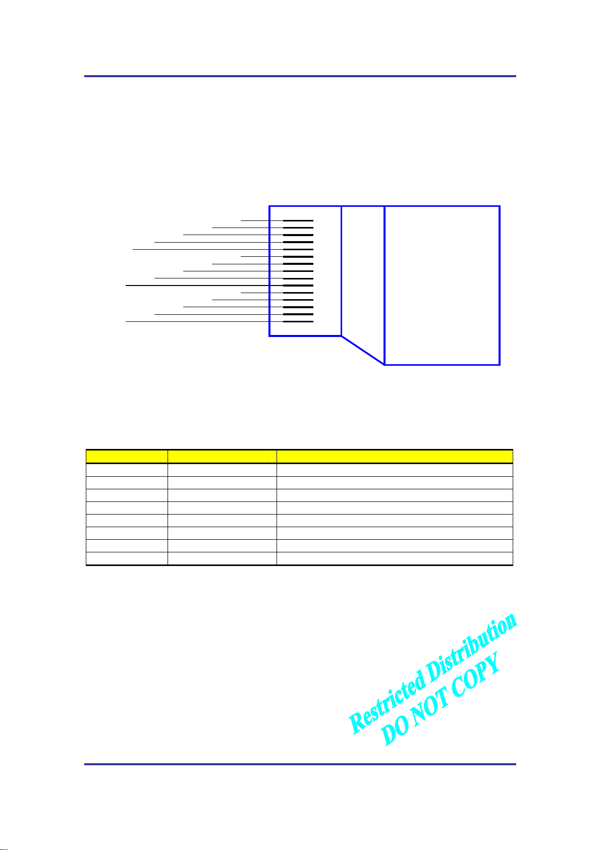
The module supports the LCD interface. The LCD interface is composed of 15-signals. Direct access
to the LCD driver is not applicable. Hence, 8-bit operation interface logic is required. The LCD interface
block diagram is shown below:
LCD_CS/
VDD
LWR /
RD/
A01
LCD_CS/
RES_OUT/
D00 ~ D07
VDD
GND
D03
NAME
D02
D07
A01
RD/
D01
D06
LWR/
D00
D05
GND
RES_OUT/
D04
GND
RW
E
RS
CS
RESET
DO
D1
D2
D3
D4
D5
D6
D7
VDD
8-Bit
Operation
Interface
Logic
Figure 4-3 LCD Interface Block Diagram
Table 4-7 LCD Interface Signals
TYPE CHARACTERISTIC
BS_PU LCD RW pin out from the module
BS LCD E pin out from the module
B LCD RS pin out from the module
O LCD Chip Select pin out from the module
O LCD Reset from the module
O LCD Data Lines from the module
LCD Power Supply
LCD Signal Ground
LCD
All Rights Reserved.
AD-2001-06-28 Ver 1.1
-22-
Page 23
AnyDATA.NET Inc. AnyTime AnyPlace Any Wireless Data Solution
4.7.3 Ringer
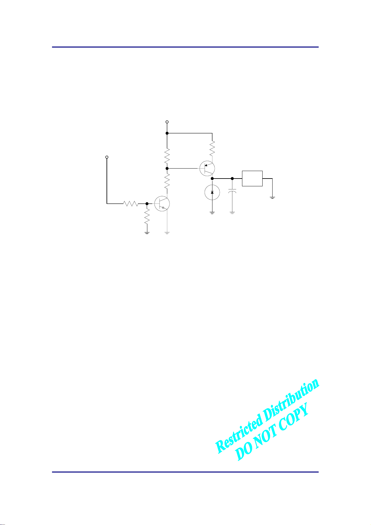
The Ringer pin provides the output to drive the sound transducer on the host. It alerts the user of a
voice call event and outputs key tones if the keypad is connected.
The reference external driver circuit is shown below:
Vdd
Ringer signal
From
the modem
10Kohm
2.2Kohm
4.7ohm
Q2
Buzzer
TM
4.7Kohm
D1
Q1
4.7Kohm
0.01uF
Figure 4-4 Reference External Ringer Driver Circuit
All Rights Reserved.
AD-2001-06-28 Ver 1.1
-23-
Page 24
AnyDATA.NET Inc. AnyTime AnyPlace Any Wireless Data Solution
TM
5. Electrical Specifications
5.1 DC Electrical Specifications
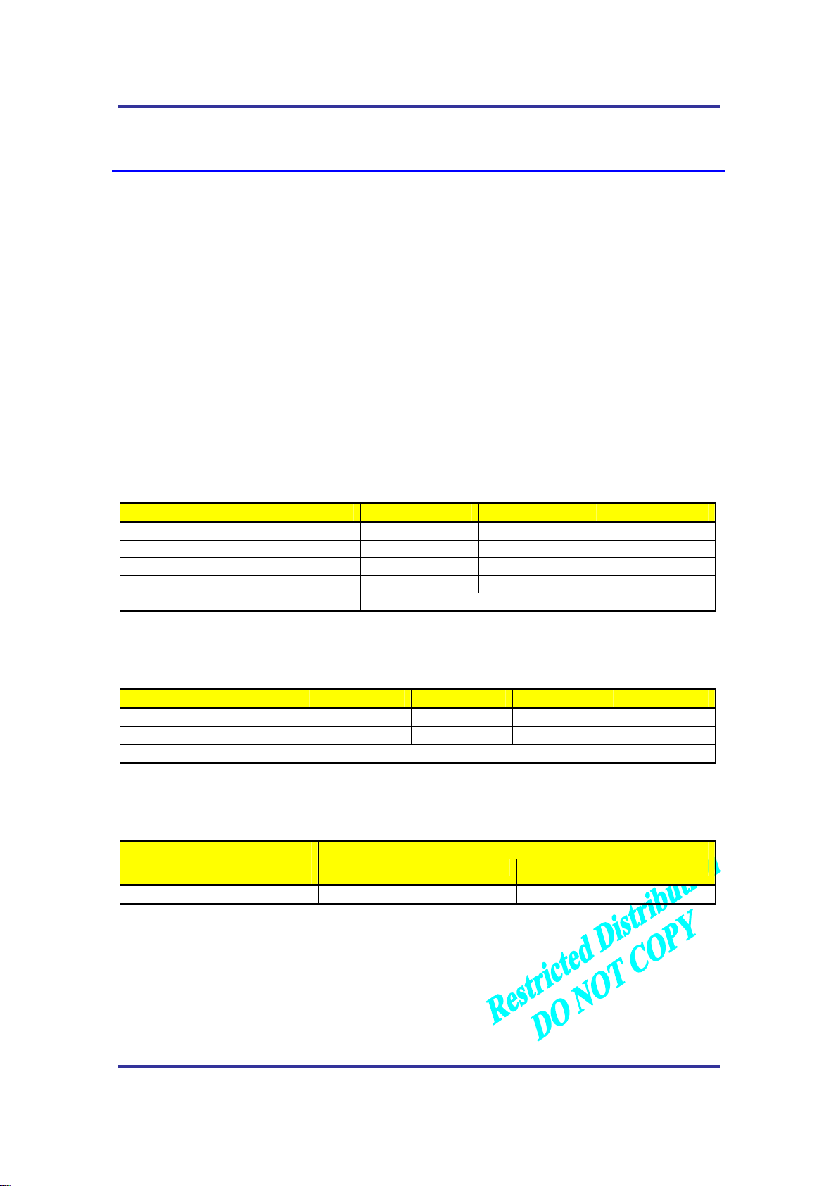
5.1.1 Absolute Maximum Ratings
Operating the module under conditions that exceed those listed in the Absolute Maximum Ratings
table may result in damage to the module.
Absolute Maximum Ratings should be considered as limiting values. The module may not function
properly and should not be operated if any one of the parameters is not within its specified operating
range.
Table 5-1 Absolute Maximum Ratings
PARAMETER MIN MAX
Storage Temperature
Voltage On Any Input or Output Pin
Supply Voltage
Initializing Current
Drop
-50 +85 ºC
-0.8 +4.8 V
-1.0 +5.0 V
250 mA
No damages after 60-Inch drop over concrete floor
UNITS
5.1.2 Recommended Operating Conditions
PARAMETER MIN TYP MAX
Supply Voltage
Operating Temperature
Operating Humidity
+3.4
-30
+3.8 +4.2 V
+60 ºC
95% (50°C) Relative Humidity
UNITS
5.1.3 Power Consumption
CONVERSATION
(Busy)
900mA (MAX)
Idle Sleep
110mA 2mA
STANDBY
All Rights Reserved.
AD-2001-06-28 Ver 1.1
-24-
Page 25
AnyDATA.NET Inc. AnyTime AnyPlace Any Wireless Data Solution
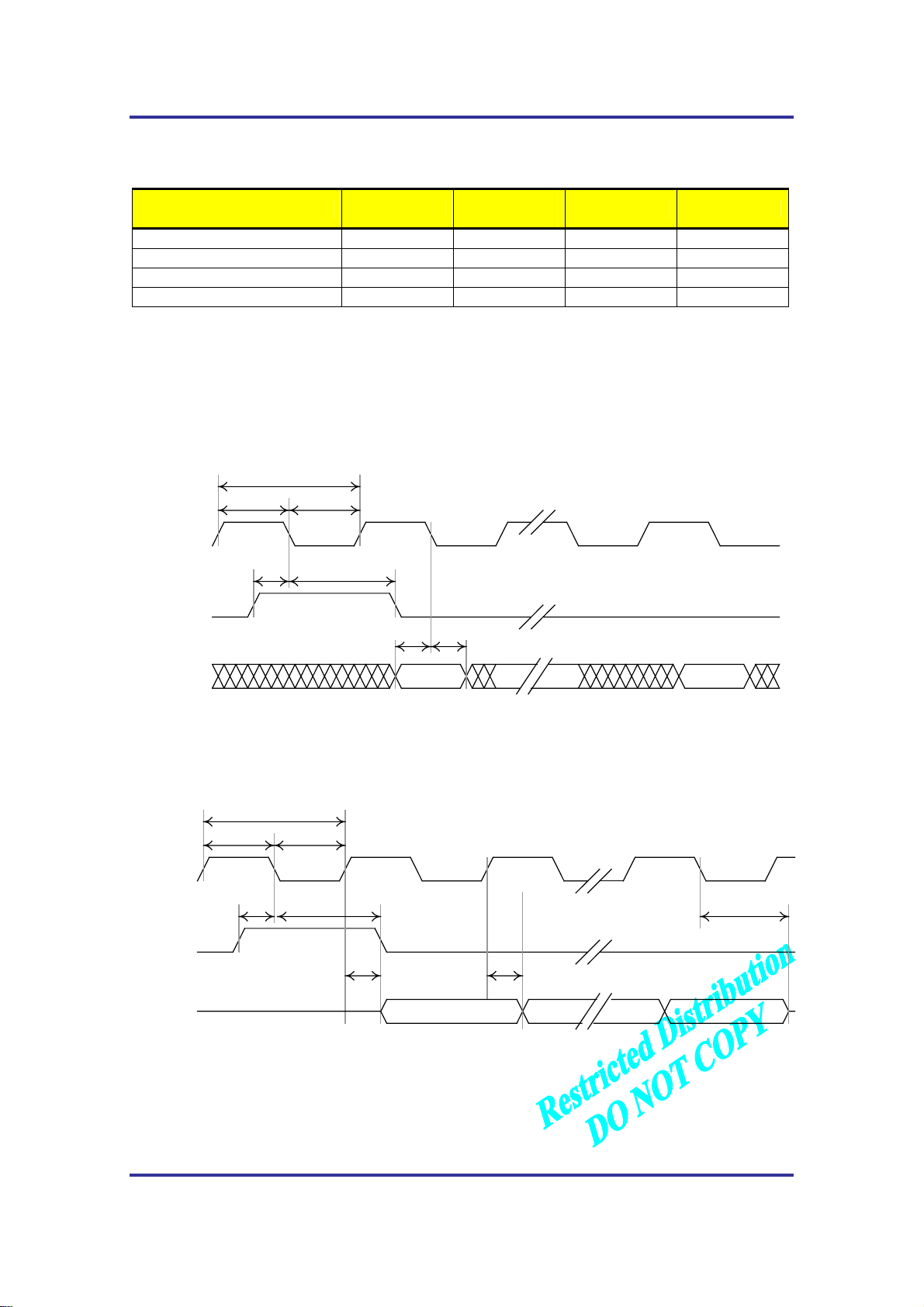
5.1.4 Serial Interface Electrical Specifications
PARAMETER MIN
Input High Voltage
Input Low Voltage
Output High Voltage
Output Low Voltage
+2.0 +3 +3.7 V
-0.5 0 +0.8 V
+2.4 +2.7 V
0 +0.4 V
TYP
(NO LOAD)
MAX
UNITS
5.2 Timing characteristics
5.2.1 External CODEC Timing
t
clk
PCM_CLK
t
clkl
t
su(sync)
t
clkh
t
h(sync)
TM
PCM_SYNC
PCM_DIN
PCM_CLK
PCM_SYNC
PCM_DOUT
t
clkl
t
t
h(din)
su(din)
MSB
Figure 5-1 External PCM CODEC to Module timing
t
clk
t
clkh
t
su(sync)
t
h(sync)
t
pdout
t
pdout
MSB LSB
LSB
t
zdout
Figure 5-2 Module to External PCM CODEC timing
All Rights Reserved.
AD-2001-06-28 Ver 1.1
-25-
Page 26
AnyDATA.NET Inc. AnyTime AnyPlace Any Wireless Data Solution
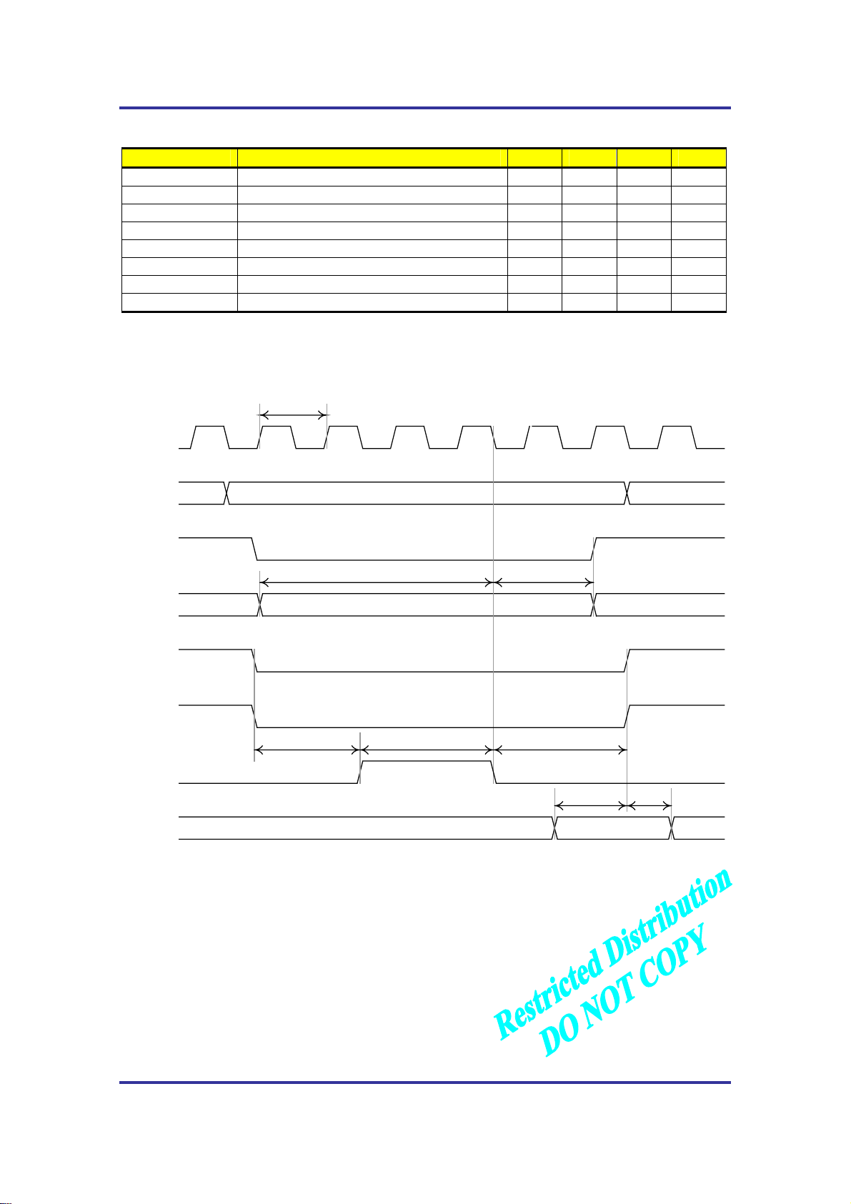
Table 5-2 External PCM CODEC Parameters
PARAMETER DESCRIPTION MIN TYP. MAX
t
clk
t
clkl
t
clkh
t
su(sync)
t
h(sync)
t
su(din)
t
h(din)
t
pdout
5.2.2 LCD Timing
MCLK
(modem)
A[21:0]
PCM-CLK cycle time 400 500 ns
PCM-CLK low time 200 250 ns
PCM-CLK high time 200 250 ns
PCM_SYNC setup time to PCM_CLK falling 150 ns
PCM_SYNC hold time after PCM_CLK falling 350 ns
PCM_DIN setup time to PCM_CLK falling 50 ns
PCM_DIN hold time after PCM_CLK falling 10 ns
Delay from PCM_CLK falling to PCM_DOUT 50 ns
T
TM
UNIT
LWR/
Write
Data[7:0]
LCD_CS/
RD/
LCD_E
Read
Data[7:0]
t
LCDES
t
WRS
LCD Data Write
t
LCDEHI
Figure 5-3 LCD Timing
t
WRH
t
LCDEH
t
RDS
LCD Data Read
t
RDH
All Rights Reserved.
AD-2001-06-28 Ver 1.1
-26-
Page 27

AnyDATA.NET Inc. AnyTime AnyPlace Any Wireless Data Solution
Table 5-3 LCD Timing Parameters
PARAMETER DESCRIPTION MIN MAX
t
LCD_CS/ active to LCD_E active
LCDES
t
LCDEHI
t
LCDEH
t
LCDEHR
t
RDS
t
RDH
t
WRS
t
WRH
Pulse width if LCD_E active ns
LCD_E inactive to LCD_CS/ inactive (write) ns
LCD_E inactive to LCD_CS/ inactive (Read)
Read data setup ns
Read data hold ns
Write data setup to LCD_E inactive ns
Write data hold from LCD_E inactive ns
ns
k, I, n is integer lower than 16, MCLK is internal Clock of module
UNIT
TM
All Rights Reserved.
AD-2001-06-28 Ver 1.1
-27-
Page 28
AnyDATA.NET Inc. AnyTime AnyPlace Any Wireless Data Solution
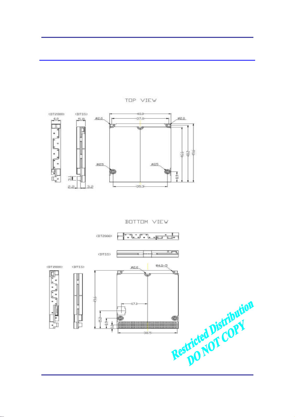
6. Mechanical Dimensions
6.1 Outline for DT2000 and DTSS series
TM
Units: mm
All Rights Reserved.
AD-2001-06-28 Ver 1.1
-28-
Page 29
AnyDATA.NET Inc. AnyTime AnyPlace Any Wireless Data Solution
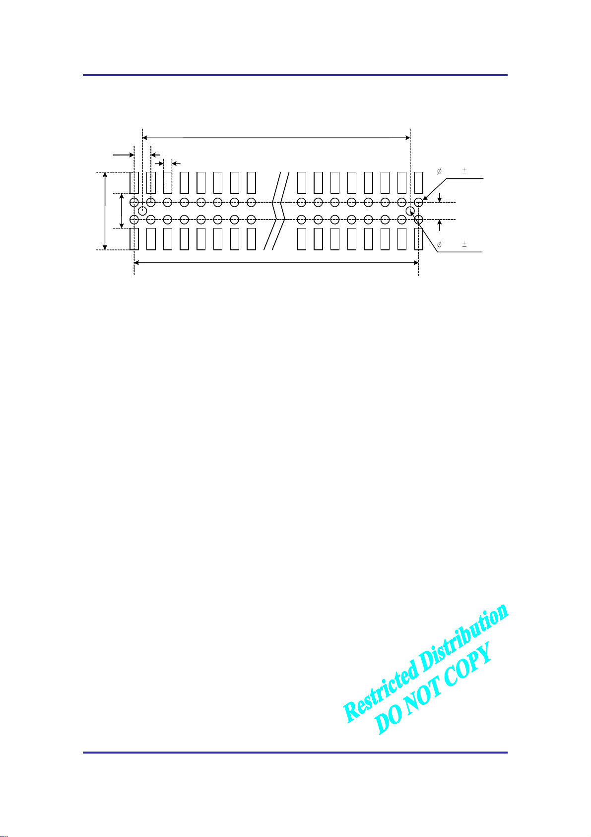
6.2 60-Pin Connector
((Pin number/2)-2)x1.27
1.27
0.55
40
0.70
0.10
TM
2.20
5.40
((Pin number/2)-1)x1.27
Figure 6-1 60-pin Female Connector (Units: mm)
Counter-Part (the 60-pin male connector (not on the DT2000-Dual)):
Part Name: Header pin connector (0.05” (1.27mm) pitch, straight, dual row)
Part Number: GDH7-60DBC-SMT
Note: For more information on the 60-pin male connector, please refer to:
http://www.goldenconnector.co.kr/index_product_e.html
Use the part name and number to help search for the correct part.
1.27
0.70
0.05
All Rights Reserved.
AD-2001-06-28 Ver 1.1
-29-
Page 30
AnyDATA.NET Inc. AnyTime AnyPlace Any Wireless Data Solution
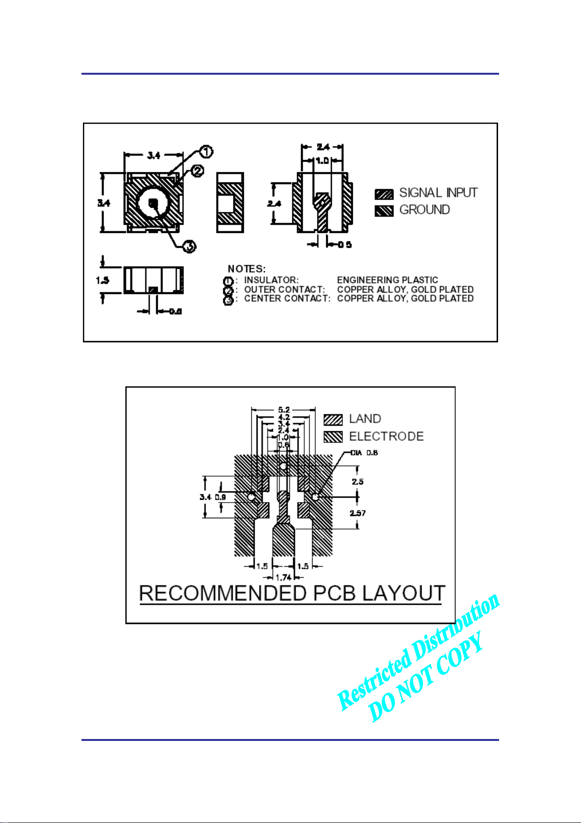
6.3 RF Connector
TM
Figure 6-2 PCB Connector (Units: mm)
Figure 6-3 PCB Connector Layout (Units: mm)
Part name: PCB Connector (RF Connector)
All Rights Reserved.
AD-2001-06-28 Ver 1.1
-30-
Page 31
AnyDATA.NET Inc. AnyTime AnyPlace Any Wireless Data Solution
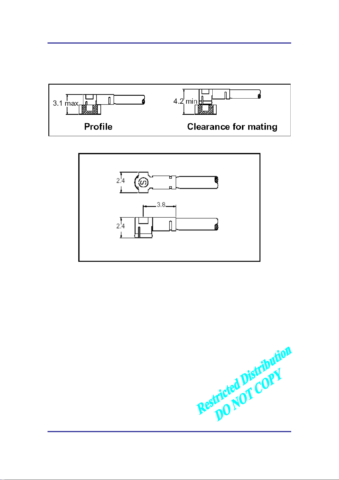
Counter-Part (not found on the DT2000-Dual) used to connect the RF connector to an antenna:
TM
Figure 6-4 Mechanical Characteristics of Cable Harness Assembly (Units: mm)
Part name: Cable Harness Assembly
Note: For more information about the RF connector parts, please refer to the file found at
http://www.sunridgecorp.com/pdf/MCAseries.pdf
All Rights Reserved.
AD-2001-06-28 Ver 1.1
-31-
 Loading...