


ANTUMBRA
FADE
MANUAL

TABLE OF CONTENTS
01. INSTALLATION 4
02. BACK 5
03. FRONT 6
04. USE 7
05. LINK 8
06. BILL OF MATERIALS 9
07. BUILD NOTES 10
08. BACK 11
09. FRONT 14
10. MODIFICATION 15
11. FINISHED 16

00. THANK YOU!
Thank you for purchasing the Antumbra FADE module!
In this documentation you can find information about the
installation and use of the module, also an assembly instruction if you got your hands on the DIY version.

01. INSTALLATION
When you turn the FADE around, you should see the module as it is on the left illustration. If this is your first FADE
POWER CABLE HEADER
103
102
104
module, connect a 10 pin header to the top row, where you
see the MAIN POWER text. Pay attention to the orientation of the cable, the RED STRIPE should be on top!
104
By doing otherwise you can potentially harm the module
104
or even your whole system! Power off your Eurorack sys-
102
LME49720
104
104
tem and connect the other end of the cable to the power
source, here also pay attention to the PSU manufacturer’s
TL072CD
instructions!
104
104
LME49720
104
104

02. BACK
LINK CABLE HEADER: Link two or more FADEs with a 16 pin
ribbon cable to send it’s output to the next FADE module.
POWER
103
102
104
103
102
104
103
102
104
You have to connect the LINK cable of the first unit to the
power header of the second unit, and so forth.
LME49720
104
104
JUMPERS:
104
104
104
102
LME49720
104
104
102
104
LME49720
104
104
102
104
104
JP3 selects the voltage range, the bottom position is 10V
TL072CD
LME49720
TL072CD
104
104
104
LME49720
104
104
104
TL072CD
LME49720
the top is 5V.
104
104
104
JP3 & JP4 selects the module’s orientation. The jumpers
104
104
104
are pointing to the bottom of the module, so if you want
to flip it, just put them both in the other position.
Both jumpers should be on either top or bottom position
at the same time.

03. FRONT
INPUT • OUTPUT
BIPOLAR • UNIPOLAR SWITCH
FADER (who knows)

04. USE
One FADE in itself can be used as an:
• Attenuator
• Offset generator
• Manual CV source
• Inverter
When there’s no input source connected, the set voltage
(on the back, 5/10V) is normalized to the input, this way
you can use it to generate CV in itself. The LED corresponds to the activity of the output, green is positive,
red is negative voltage. If you switch to BIPOLAR mode,
0V will be in the center of the fader, down is negative
voltage, up is positive.
When you connect an input source you can attenuate it
with the fader.

OUT
OUT
IN1 IN4
IN2 IN3
MIX
IN4 OFFSET
05. LINK
FADE gets more interesting if you LINK more units, this
way you can mix signals together, or offset them easily.
To mix signals, insert a cable in the output of only the last
unit you want in the chain, this breaks the normalization
and the signal won’t appear further down the chain. You
can set up a master volume by connecting the output of
the module before the last one to the last one’s, so that
the last fader attenuates the mixed signal.
If you connect an input source in unit 1, and no input to
unit 2, you can use unit 2 as an offset for the signal, great
for LFOs, envelopes, etc.

06. BILL OF MATERIALS
QTY PART
2 1K RESISTOR (0603 SMD • 1%)
1 10K RESISTOR (0603 SMD • 1%)
9 100K RESISTOR (0603 SMD • 0.1% • THIN FILM)
6 100NF CAPACITOR (0603 SMD • >= 16V)
1 22PF CAPACITOR (0603 SMD • <= 2%, >= 25V)
2 10UF ELECTROLYTIC CAPACITOR (SMD • >= 25V)
2 1N5819HW DIODE (SOD123)
1 LM4040 (SOT23 • 10V)
1 TL072 DUAL OP-AMP (SOIC8)
QTY PART
3 JUMPER (2.54MM LEAD SPACING)
1 10MM SPACER
2 THONKICONN JACK
2 M3X5 SCREW
1 SLIDE POT KNOB
DETAILED EXCEL SHEET WITH PART NAMES, NUMBERS
AND LINKS: HERE
2 LME49720 DUAL OP-AMP (SOIC8)
1 LM321MF (SOT23-5)
1 SLIDE POT (B10K)
1 LED (3MM • RED/GREEN • 2 TERMINALS)
2 2X8 MALE HEADER (2.54MM LEAD SPACING)
3 1X3 MALE HEADER (2.54MM LEAD SPACING)
MOUSER CART: HERE
NOTE: jacks, screw and pot knob is not included in the
cart! See the excel sheet about these.

07. BUILD NOTES
Before you start building look through the build manual
so that you’ll be familiar with the building process and
you won’t run into any surprises! :)
Good luck!

08. BACK
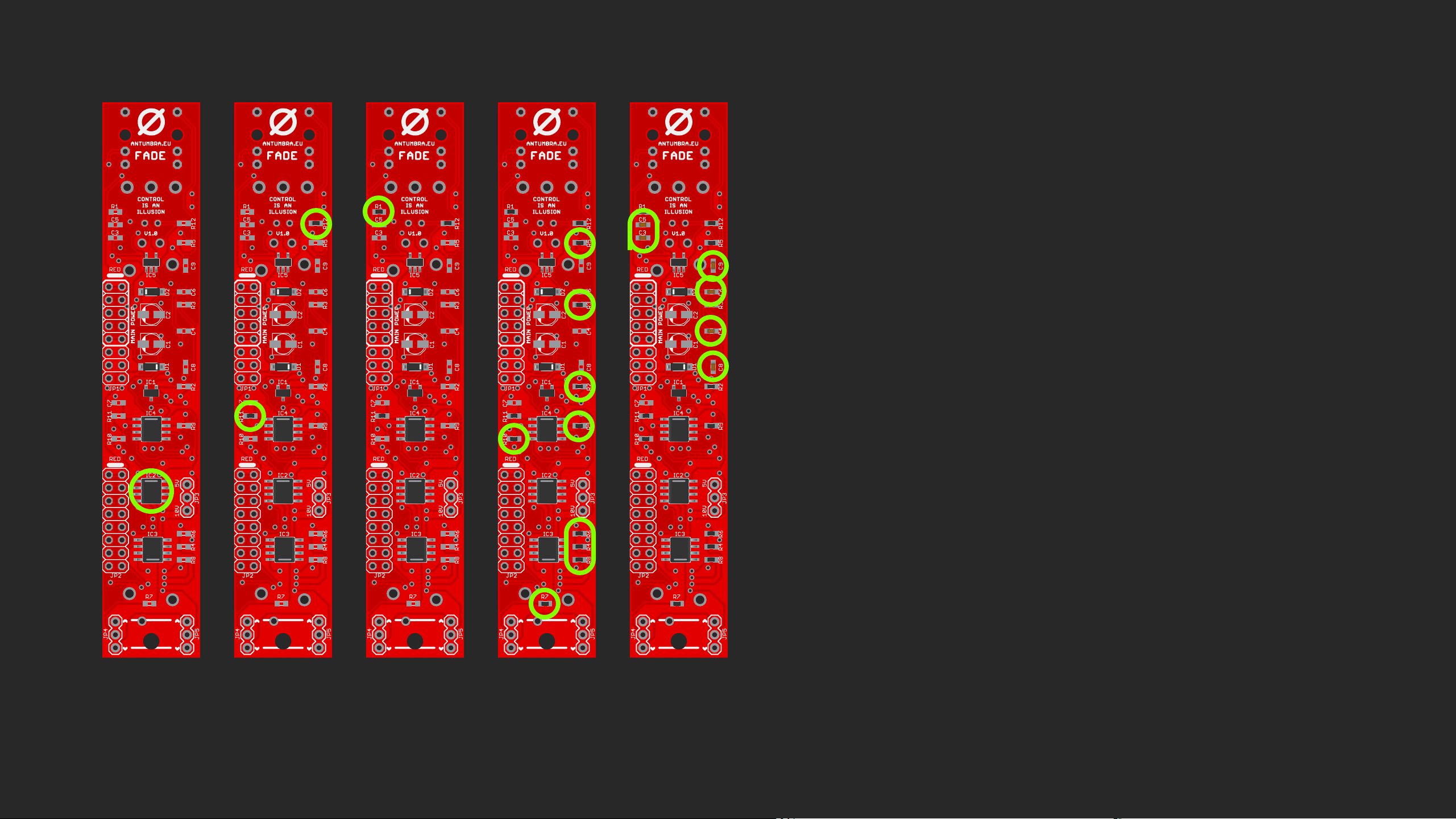
00. Orient the PCB as seen on the left.
01. Solder the LM321MF.
02. Solder the diodes, check the marking on them, they
should align with the white lines as on the graphic.
00 01 02 0403
LME49720
LME49720
03. Solder the LM4040.
04. Solder the two LME49720 opamps, their orientation
can be determined by the slope on one of it’s sides.
They should align up with the line on the PCB.
08. BACK
05. Solder the single TL072 IC, it’s orientation is deter-
LME49720
TL072CD
LME49720
103
102
102
103
102
104
103
102
104
mined as the previous IC-s (but usually it also has a
marking on the top).
104
104
06. Solder the two 1K resistors.
104
104
07. Solder the single 10K resistor.
102
LME49720
102
LME49720
102
LME49720
104
104
102
LME49720
104
104
08. Solder the nine 100K resistors.
TL072CD
LME49720
TL072CD
LME49720
TL072CD
LME49720
TL072CD
104
104
104
LME49720
104
104
104
09. Solder the six 100nF capacitors.
104
05 06 07 0908
104
08. BACK
10. Solder the single 22pF capacitor.
103
102
104
103
102
104
103
102
104
103
102
104
11. Solder the two 10uF electrolytic capacitors, their orientation matter! The black line on them should face
104
104
104
104
to the left.
104
104
104
104
12. Solder the 2x8 pin headers.
102
104
LME49720
104
102
LME49720
104
104
102
LME49720
104
104
102
LME49720
104
104
On the top header (JP1) snip off the 6th row pins so
that you can connect the 10 pin header. This is only
TL072CD
TL072CD
TL072CD
TL072CD
necessary for the first module in the chain, alternatively you can just install a 2x5 header if you are very
sure it’ll be chained (and that it will be the first).
LME49720
LME49720
104
104
104
104
104
104
LME49720
104
104
104
LME49720
104
104
104
104
104
104
104
10 11 12 13
If you have the PCB v1.0, you’ll have to make a bit of modification to make it work with
versions v1.1 and above. Learn about this in section 11.
13. Solder the three 1x3 pin headers. You can already insert the jumpers if you like, as described in section 2.

09. FRONT
00. Orient the PCB as it is seen on the left.
01. Solder the fader in place. (there should only be one
possible way to insert it)
02. DO NOT SOLDER YET!
Add the:
• jacks
00 01 02 03
• switch (orientation doesn’t matter)
• LED
• Spacer (screw it to the PCB)
03. Put the panel on top, screw it to the spacer and add
the nuts to the jacks, align the switch and LED nicely,
as you like it. Then solder everything in place.

CONNECT
10. MODIFICATION
If the version number of your PCB is v1.0, you have to
make a small modification to make it work with versions
above it.
You only have to connect pin row 6 to pin row 8 with some
wire on both headers as seen on the image to the left.
You also have to connect the pins next to eachother with
some solder.
CONNECT
That’s it!

11. FINISHED
You are now finished with building the module, congratulations for your new awesome FADE!
Now you can go back to section 2. to connect the unit to a
power source and set up the jumpers as you like it.
 Loading...