

APW7060
Dual Controllers - Step Down Synchronous PWM and Linear Controller
Features
••
Provides Two Regulated Voltages
•
••
- One Synchronous DC/DC Buck Controller
- One Linear Controller
••
0.8V Internal Reference Voltage
•
••
- Both Controllers: 0.8V ± 2% Line, Load
and Temp.
••
Output Voltage Range
•
••
- PWM Controller : 0.8V to V
- Linear Controller : 0.8V to (12VCC-V
••
• Full Duty Cycle Range for PWM Controller
••
IN
)
GSpass
- 0% to 100%
••
• Internal Loop Compensation for PWM Controller
••
••
• Internal 2ms Soft Start and Short Circuit Protec
••
tion for both Controllers
••
• Both Controllers Drive N-Channel MOSFETs
••
••
• Small Converter Size
••
- 600kHz Constant Switching Frequency
- Simple SO-14 Package
••
• Shutdown Control
••
Applications
••
• Motherboard
••
••
• Graphics Cards
••
General Description
The APW7060 integrates a synchronous buck PWM
controller and a linear controller to provide two regulated voltages in a single package. The PWM controller drives external N-channel MOSFETs and operates
at a fixed 600kHz frequency. When the input supply
drops close to the output, the upper MOSFET remains
on, achieving 100% duty cycle. Internal loop compensation is optimized for fast transient response, eliminating external compensation network. The linear controller drives an external N-channel MOSFET to form a
linear regulator. The internal 0.8V reference makes this
part suitable for a wide variety of low voltage
applications.
The APW7060 has an undervoltage lockout circuitry
to ensures that both the 5VCC and 12VCC must be
present before its internal circuitry is power up. Soft
start is internally set to 2ms and will bring both outputs into regulation in a controlled manner. When either output goes into short, soft start will be initiated.
If the short condition still remains after three cycles,
both regulators will be shut down. To restart both
regulators, recycle the voltage at 5VCC or 12VCC pin
or momentarily pull the FB2 pin above 1.28V.
The APW7060 can be shutdown by pulling the FB2
pin above 1.28V. In shutdown, all gate drive signals
will be low. This dual controller is available in SO-14
package.
Pinouts
FB2
NC
1
2
3
4
5
6
7
••
• 12V , 5V and 3.3V Inputs DC-DC Converter
••
••
• DSP Supplies
••
••
• Embedded processor and I/O supplies
••
ANPEC reserves the right to make changes to improve reliability or manufacturability without notice, and advise
customers to obtain the latest version of relevant information to verify before placing orders.
Copyright ANPEC Electronics Corp.
Rev. A.3 - Oct., 2003
LGATE
GND
GND
5VCC
DRIVE2
UGATE
14
13
12VCC
NC
12
NC
11
NC
10
FB
9
NC
8
www.anpec.com.tw1
APW7060
Ordering and Marking Information
APW 7060
APW7060 K :
APW7060
XXXXX
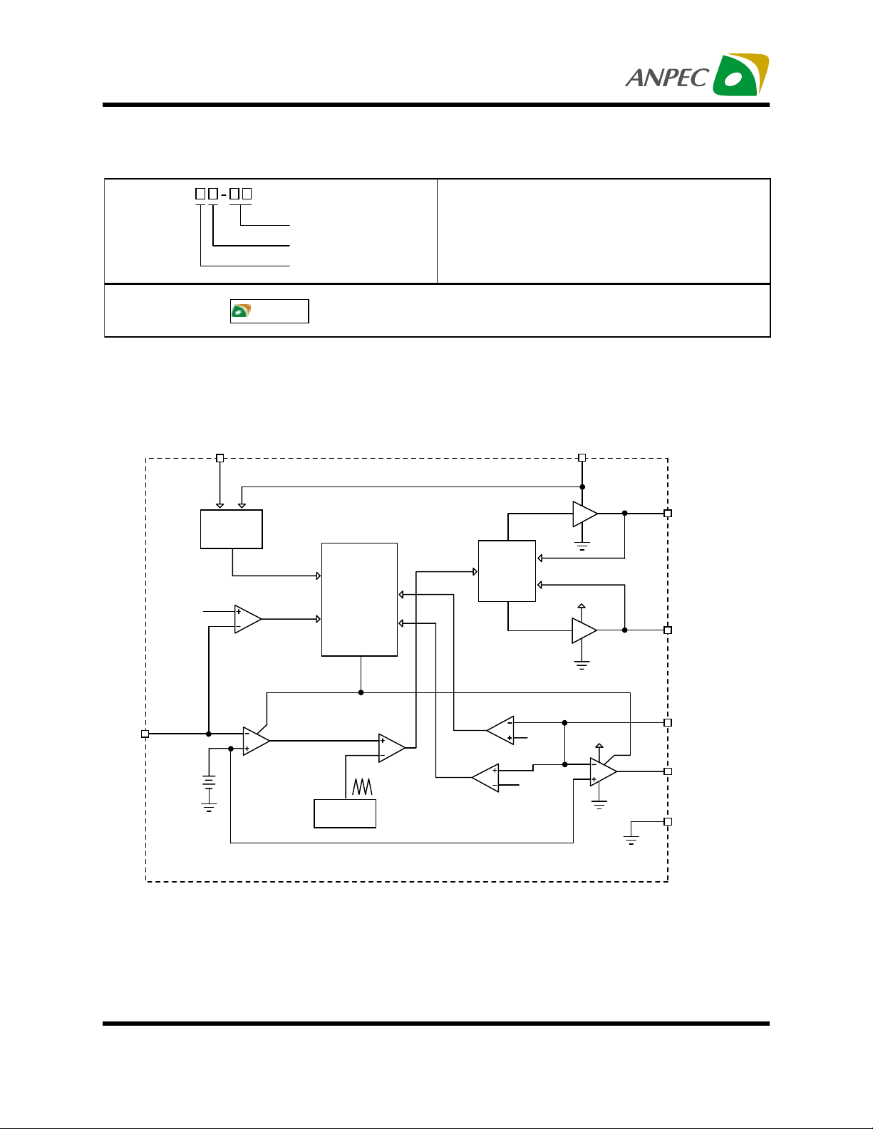
Block Diagram
5VCC
Under
Voltage
Lockout
UVLO
0.5V
Handling Code
Temp. Range
Package Code
UVP1
Soft-Start
and Fault
Logic
Packag e Cod e
K : S OP-1 4
Operating Junction Temp. Range
C : 0 to 7 0 °C
Handling Code
TU : T u be
TR : T a pe & R e e l
XXXXX - Date Code
12VCC
PWM
Gate
Control
UGATE
5VCC
LGATE
FB
VREF
0.8V
COMP
Error
Amplifier
Copyright ANPEC Electronics Corp.
Rev. A.3 - Oct., 2003
Inhibit /
Soft-Start
Os c illa t or
.ECKH/Figure 1.
F
OSC
600kHz
UVP2
Shutdown
0.5V
1.28V
12VCC
Linear
Controller
FB2
DRIVE2
GND
www.anpec.com.tw2
APW7060
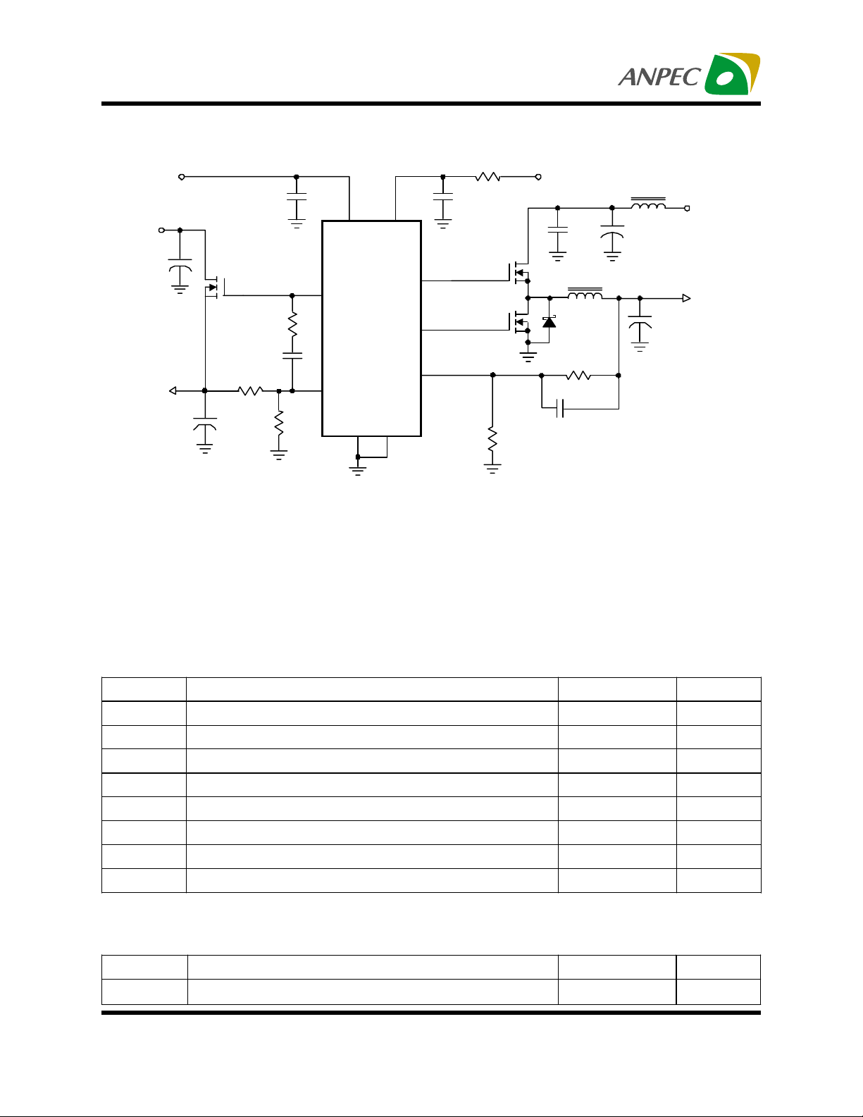
Typical Application
+12V
V
IN2
+3.3V
C10
470uF
V
OUT2
+2.5V/3A
C11
470uF
Q1 : APM2014N UC
Q2 : APM2014N UC
Q3 : APM2055N UC
D1 : 3A Schottky Diode
C2, C3, C5, C6, C10, C1 1 : 470uF/6.3V, ESR=30mΩ
Q3
R10
6.8k
C9
470pF
R7
2.37k R8
1.13k
C8
1uF
5
6
12VC C
DR IVE2
FB2
13
U1
APW 7060
GND
2
5VC C
UGATE
LGATE
GND
R4
+5V
2.2
C1
4
1uF
C4
4.7uF
Q1
14
L1
1uH
L2
1uH
C2, C3
2 x 470uF
V
IN1
+3.3V
V
OUT1
+1.263V
1
Q2
9
FB
3
R2
1.02k
D1
C7
68nF
C5, C6
2 x 470uF
R1
590
/10A
.ECKH/Figure 2.
Absolute Maximum Ratings
Symbol Parameter Rating Unit
5V
12V
5VCC Supply Voltag e ( 5 V CC to GND) -0.3 ~ 7 V
CC
12VCC Supply Voltage (12VCC to GND) -0.3 ~ 15 V
CC
UAGTE, DRIVE2 to GND -0.3 ~ 12V
LGATE, FB, FB2 to GND -0.3 ~ 5V
CC
CC
Maximum Junction Temperature 150
T
STG
T
SDR
V
ESD
Storage Temperature -65 ~ 150
Maximum Soldering Temperature, 10 Seconds 300
Minimum ESD R ating (Human b ody model)
2
±
Thermal Characteristics
Symbol Parameter Value Unit
JA
θ
Junction-to-Ambient Resistance in free air (SOP-14) 160
o
o
o
KV
o
C/W
V
V
C
C
C
Copyright ANPEC Electronics Corp.
Rev. A.3 - Oct., 2003
www.anpec.com.tw3
APW7060
Recommended Operating Conditions
(Note)
Symbol Parameter Range Unit
CC
5V
12V
OUT1
V
V
OUT2
V
V
T
T
IN1
IN2
A
5VCC Supply Voltage
CC
12VCC Supply Voltage
5 ± 5%
12 ± 10%
Output Voltage of the Buck converter 0.8 ~ 3.3 V
Input Voltage of the Buck converter
3.3/5 ± 5%
Output Voltage of the Linear Regulator 0.8 ~ 3.3 V
Input Voltage of the Linear Regulator
3.3/5 ± 5%
Ambient Temperature 0 ~ 70
J
Junction Temperature 0 ~ 125
V
V
V
V
o
C
o
C
Note : Refer to the typical application circuit
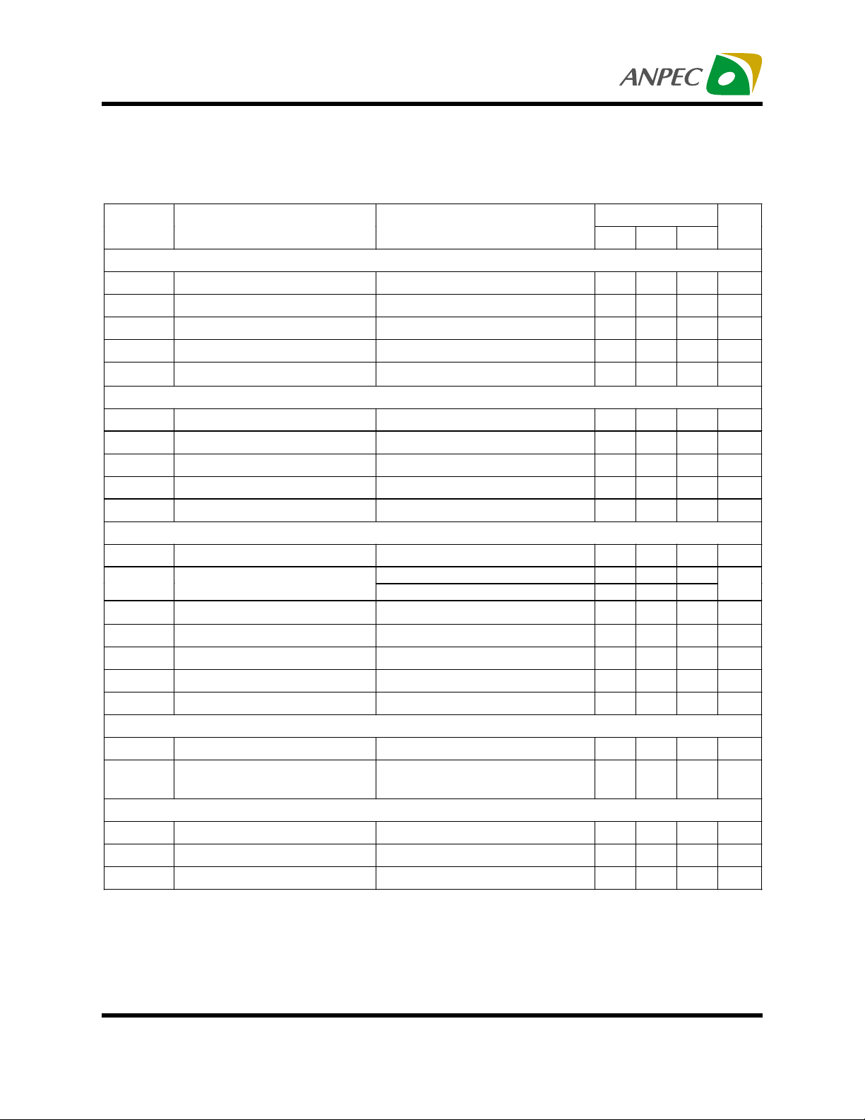
Electrical Characteristics
Unless otherwise specified, these specifications apply over 5VCC=5V, 12VCC=12V and TA= 0~70 oC. Typical
values are at TA=25oC.
APW7060
Symbol Parameter Test Conditions
Min Typ Max
SUPPLY CURRENT
ICC 5VCC Supply Current
12VCC Supply Current
LGATE Open, FB2=DRIVE2
UGATE Open
2.5 mA
2.5 mA
UNDER VOLTAGE LOCKOUT
Rising 5VCC Threshold 12VCC=12V 4.0 4.2 4.4 V
Falling 5VCC Threshold 12VCC=12V 3.5 3.7 3.9 V
Rising 12VCC Threshold 5VCC=5V 9.6 10.3 10.8 V
Falling 12VCC Threshold 5VCC=5V 9.3 9.7 10.2 V
OSCILLATOR
OSC
F
Free Running Frequency 550 600 650 kHz
Ramp Upper Threshold 2.85 V
Ramp Lower Threshold 0.95 V
Ramp Amplitude 1.9 V
OSC
∆V
REFERENCE VOL TAGE
REF
V
Reference Voltage 0.8 V
System Accura cy
Over Line, Load and
Temperature
-2 +2 %
Unit
P-P
Copyright ANPEC Electronics Corp.
Rev. A.3 - Oct., 2003
www.anpec.com.tw4
APW7060
Electrical Characteristics (Cont.)
Unless otherwise specified, these specifications apply over 5VCC=5V, 12VCC=12V and TA= 0~70 oC. Typical
values are at TA=25oC.
Symbol Parameter Test Conditions
BUILT-IN PWM FEEDBACK COMPENSATION
DC Gain 75 dB
P
F
F
First Pole Frequency 10 Hz
Z
First Zero Frequency 1
UGATE Duty Range 0 100 %
FB Input Current
PWM CONTROLLER GATE DRIVERS
UGATE Source V
UGATE Sink
LGATE Source V
LGATE Sink V
D
T
Dead Time 50
UAGTE
=1V 0.6 A
UGATE
V
=1V 7.3
LGATE
=1V 0.6 A
LGATE
=1V 1.8
LINEAR CONTROLLER
DC Gain 78 dB
Gain Bandwidth Product
CL=0.5nF 1.6
L
C
=1nF 1
FB Input Current 0.1
DRIVE2 S ourc e C ur re nt V
DRIVE2 Sink Current V
FB2=VREF
FB2=VREF
-20mV, V
+20mV, V
DRIVE2
DRIVE2
DRIVE2 Output High Vo ltage DRIVE2 Open 11.7 V
DRIVE2 Output Low Voltage DRIVE2 Ope n 0.01 V
UNDER-VOLTAGE PROTECTION
FB
UV
FB/FB2 Under-Voltage Level FB or FB2 Falling 0.5 V
FB/FB2 Under-Voltage
Hysteresis
15 mV
SOFT-START AND SHUTDOWN
SS
T
Soft-Start Interval 2 mS
FB2 Shutdown Threshold FB2 Rising 1.28 V
FB2 Shutdown Hysteresis 30 mV
APW706 0
Unit
Min Typ Max
kHz
0.1
µA
Ω
Ω
nS
MHz
µA
=7V 9.8 mA
=3V 2.6
mA
Copyright ANPEC Electronics Corp.
Rev. A.3 - Oct., 2003
www.anpec.com.tw5

APW7060
Functional Pin Description
LGA TE (Pin 1)
This pin provides the gate drive signal for the low side
MOSFET .
GND (Pin 2, 3)
Signal and power ground for the IC. All voltage levels
are measured with respect to this pin. Tie this pin to
the ground plane through the lowest impedance connection available.
5VCC (Pin 4)
This is the main bias supply for the DC/DC controller
and its low side MOSFET driver. Must be closely
decoupled to GND (Pin 2,3). The voltage at this pin is
monitored for undervoltage lockout (UVLO) purposes.
DO NOT apply a voltage greater than 5.5V to this pin.
DRIVE2 (Pin 5)
This pin provides the gate drive voltage for the linear
regulator N-channel MOSFET pass transistor. It also
provides a means of compensating the linear controller for applications where the user needs to optimize
the regulator transient response.
NC (Pin 7, 8, 10, 11, 12)
No internal connection.
FB (Pin 9)
This pin is the inverting input of the internal error amplifier of the buck controller. Connect this pin to the
output (VOUT1) of the DC/DC converter via a proper sized
resistor divider to form a complete feedback loop. The
VOUT1 is determined using the following formula :
VOUT1=0.8V x (1+ )
where R1 is the resistor connected from VOUT1 to FB,
and R2 is the resistor connected from FB to GND.
This pin is also monitored for under-voltage events.
12VCC (Pin 13)
This pin provides the supply voltage to the high side
MOSFET driver and the linear controller. A voltage no
greater than 13V can be connected to this pin. The
voltage at this pin is monitored for undervoltage lockout (UVLO) purposes.
UGATE (Pin 14)
R1
R2
FB2 (Pin 6)
Connect this pin to the output (VOUT2) of the linear
regulator via a proper sized resistor divider. The voltage at this pin is regulated to 0.8V and the VOUT2 is
determined using the following formula :
VOUT2=0.8V x (1+ )
where R7 is the resistor connected from VOUT2 to FB2,
and R8 is the resistor connected from FB2 to GND.
This pin is also monitored for under-voltage events.
Pulling and holding FB2 above 1.28V shuts down both
regulators. Releasing FB2 initiates soft-start on both
regulators.
Copyright ANPEC Electronics Corp.
Rev. A.3 - Oct., 2003
R7
R8
This pin provides gate drive for the high-side MOSFET.
www.anpec.com.tw6

APW7060
Typical Characteristics
Reference Voltage
vs. Junction Temperature
0.816
0.812
0.808
0.804
0.800
0.796
0.792
0.788
Reference Voltage, VREF (V)
0.784
-50 -25 0 25 50 75 100 125 150
Junction Temperature (oC)
Switching Frequency
vs. Junction Temperature
650
640
630
620
610
600
590
580
570
560
Switching Frequency, FOSC (kHz)
550
-50 -25 0 25 50 75 100 125 150
Junction Temperature (°C)
Copyright ANPEC Electronics Corp.
Rev. A.3 - Oct., 2003
www.anpec.com.tw7

APW7060
Operating Waveforms (Refer to the typical application circuit)
1.V
OUT1 Load Transient Response : IOUT = 0A -> 10A -> 0A
- IOUT1 slew rate = ±10A/µS
IOUT = 0A -> 10A
IOUT = 0A -> 10A -> 0A
I
OUT = 10A -> 0A
V
OUT1
V
UGATE
10A
I
OUT1
0A
Ch1 : VOUT1, 100mV/Div, DC,
Offset = 1.25V
Ch2 : VUGATE, 10V/Div , DC
Ax1 : IOUT1, 5A/Div
Time : 5µS/Div
Ch1 : VOUT1, 100mV/Div, DC,
Offset = 1.25V
Ax1 : IOUT1, 5A/Div
Time : 100µS/Div
BW = 20MHz
BW = 20MHz
2.VOUT2 Load Transient Response : IOUT = 0.2A -> 3A -> 0.2A
- IOUT2 slew rate = ±3A/µS
IOUT = 0.2A -> 3A
IOUT = 0.2A -> 3A -> 0.2A
V
I
OUT1
OUT1
Ch1 : VOUT1, 100mV/Div, DC,
Offset = 1.25V
Ch2 : VUGATE, 10V/Div , DC
Ax1 : IOUT1, 5A/Div
Time : 5µS/Div
BW = 20MHz
IOUT = 3A -> 0.2A
V
V
I
OUT1
UGATE
OUT1
V
OUT2
I
OUT2
Ch1 : VOUT2, 50mV/Div, DC,
Offset = 2.50V
Ax1 : IOUT2, 1A/Div
Time : 1µS/Div
BW = 20MHz
Copyright ANPEC Electronics Corp.
Rev. A.3 - Oct., 2003
V
OUT2
0.2A
Ch1 : VOUT2, 50mV/Div, DC,
Offset = 2.50V
Ax1 : IOUT2, 1A/Div
Time : 50µS/Div
BW = 20MHz
3A
I
OUT2
Ch1 : VOUT2, 50mV/Div, DC,
Offset = 2.50V
Ax1 : IOUT2, 1A/Div
Time : 1µS/Div
BW = 20MHz
www.anpec.com.tw8
V
I
OUT2
OUT2

APW7060
Operating Waveforms (Cont.)
3. Powering ON / OFF
Soft-start at Powering ON
Ch1 : +5V, 1V/Div, DC
Ch2 : +12V, 2V/Div, DC
Ch3 : VOUT1, 1V/Div, DC
Ch4 : VOUT2, 1V/Div, DC
Time : 1mS/Div
BW = 20MHz
4. UGA TE and LGATE
+12V
+5V
VOUT2
VOUT1
Powering OFF
+12V
+5V
VOUT2
VOUT1
Ch1 : +5V, 1V/Div, DC
Ch2 : +12V, 2V/Div, DC
Ch3 : VOUT1, 1V/Div, DC
Ch4 : VOUT2, 1V/Div, DC
Time : 5mS/Div
BW = 20MHz
UGA TE Rising
IOUT=10A
VLGA TE
Ch1 : VUGATE, 2V/Div , DC
Ch2 : VLGATE, 2V/Div , DC
Time : 50nS/Div
BW = 500MHz
Copyright ANPEC Electronics Corp.
Rev. A.3 - Oct., 2003
VUGA TE
UGA TE Falling
IOUT=10A
VUGA TE
VLGA TE
Ch1 : VUGATE, 2V/Div, DC
Ch2 : VLGATE, 2V/Div , DC
Time : 50nS/Div
BW = 500MHz
www.anpec.com.tw9

APW7060
Application Information
Soft Start
Soft start can be initiated in several ways. One way is
when the input bias supply to the 5VCC and 12VCC
is above 4.2V and 10.2V respectively. The other way
is when the part comes out of shutdown. In both ways,
the soft start cycle will last for 2ms. During this period,
the reference to the error amplifier of the PWM controller and linear controller will gradually slew up to its
final value of 0.8V. This effectively will force both output voltages to track this reference ramp rate. Hence
both outputs will reach regulation at the same time.
Figure 3 illustrates this graphically.
Soft-start at Powering ON
+12V
+5V
VOUT2
VOUT1
Ch1 : +5V, 1V/Div, DC
Ch2 : +12V, 2V/Div, DC
Ch3 : VOUT1, 1V/Div, DC
Ch4 : VOUT2, 1V/Div, DC
Time : 1mS/Div
BW = 20MHz
.ECKH/Figure 3.
Linear Regulator Transient Response Optimization
The linear regulator is stable over all load current.
However, the transient response can be further enhanced by connecting a RC network between the FB2
and DRIVE2 pin. Depending on the output capacitance
and load current of the application, the value of this
RC network is then varied. A good starting point for
the resistor value is 6.8kΩ and 470pF for the capacitor.
Maximum Output Voltage of Linear Controller
The maximum drive voltage at DRIVE2 is determined
by the applied voltage at 12VCC pin. Since this pin
drives an external N-channel pass MOSFET, therefore the maximum output voltage of the linear regulator is dependent upon the required gate-to-source voltage to sustain the load current.
V
OUT2MAX
= 12VCC - V
GSpass
Component Selection Guidelines
PWM Regulator Output Capacitor
The selection of C
is determined by the required
OUT
effective series resistance (ESR) and voltage rating
rather than the actual capacitance requirement. Therefore select high performance low ESR capacitors that
are intended for switching regulator applications. In
some applications, multiple capacitors have to be
paralled to achieve the desired ESR value. If tantalum
capacitors are used, make sure they are surge tested
by the manufactures. If in doubt, consult the capacitors manufacturer.
Input Capacitor Selection
The input capacitor is chosen based on the voltage
rating and the RMS current rating. For reliable
operation, select the capacitor voltage rating to be at
least 1.3 times higher than the maximum input voltage.
The maximum RMS current rating requirement is approximately I
/2 , where I
OUT
is the load current.
OUT
During power up, the input capacitors have to handle
large amount of surge current. If tantalum capacitors
are used, make sure they are surge tested by the
manufactures. If in doubt, consult the capacitors
manufacturer.
For high frequency decoupling, a ceramic capacitor
between 0.1uF to 1uF can be connected between
5VCC and ground pin.
Copyright ANPEC Electronics Corp.
Rev. A.3 - Oct., 2003
www.anpec.com.tw10

APW7060
Application Information
Inductor Selection
The inductance of the inductor is determined by the
output voltage requirement. The larger the inductance,
the lower the inductor’s current ripple. This will translate into lower output ripple voltage. The ripple current
and ripple voltage can be approximated by:
OUT
V
OUT-IN
VV
RIPPLE
×
V
L Fs
×
x ESR
IN
I
RIPPLE
∆V
OUT
=
= I
where Fs is the switching frequency of the regulator.
There is a tradeoff exists between the inductor’s ripple
current and the regulator load transient response time
A smaller inductor will give the regulator a faster load
transient response at the expense of higher ripple current and vice versa. The maximum ripple current occurs at the maximum input voltage. A good starting
point is to choose the ripple current to be approximately 30% of the maximum output current.
Once the inductance value has been chosen, select
an inductor that is capable of carrying the required
peak current without going into saturation. In some
type of inductors, especially core that is make of
ferrite, the ripple current will increase abruptly when it
saturates. This will result in a larger output ripple
voltage.
P
UPPER
P
LOWER
where I
2
= I
(1+ TC)(R
out
2
= I
(1+ TC)(R
out
is the load current
OUT
DS(ON)
DS(ON)
)D + (0.5)(I
)(1-D)
)(VIN)(tsw)F
out
TC is the temperature dependency of R
S
DS(ON)
FS is the switching frequency
t
is the switching interval
sw
D is the duty cycle
Note that both MOSFET s have conduction losses while
the upper MOSFET include an additional transition
loss.The switching internal, t
reverse transfer capacitance C
, is a function of the
sw
. Figure 4 illustrates
RSS
the switching waveform of the MOSFET.
The (1+TC) term is to factor in the temperature dependency of the R
“R
vs T emperature” curve of the power MOSFET.
DS(ON)
and can be extracted from the
DS(ON)
Linear Regulator Input/Output Capacitor Selection
The input capacitor is chosen based on its voltage
rating. Under load transient condition, the input capacitor will momentarily supply the required transient
current. A 1uF ceramic capacitor will be sufficient in
most applications.
The output capacitor for the linear regulator is chosen
to minimize any droop during load transient condition.
In addition, the capacitor is chosen based on its voltage rating.
PWM Regulator MOSFET Selection
The selection of the N-channel power MOSFETs are
determined by the R
(C
) and maximum output current requirement.The
RSS
, reverse transfer capacitance
DS(ON)
losses in the MOSFETs have two components: conduction loss and transition loss. For the upper and
lower MOSFET, the losses are approximately given
by the following :
Copyright ANPEC Electronics Corp.
Rev. A.3 - Oct., 2003
Linear Regulator MOSFET Selection
In addition to choosing the pass MOSFET for its ability to sustain the load current requirement (see Maximum Output Voltage of Linear Controller), another criteria is its efficiency of heat removal. The power dissipated by the MOSFET is given by:
Pdiss = Iout * (VIN - V
OUT2
)
www.anpec.com.tw11

APW7060
Application Information
where Iout is the maximum load current
V
is the nominal output voltage
out2
In some applications, heatsink maybe required to help
maintain the junction temperature of the MOSFET below its maximum rating.
V
DS
Voltage a cro ss
drain and source of MOSFET
t
sw
Figure 4. Switching waveform across MOSFET
Layout Considerations
In high power switching regulator, a correct layout is
important to ensure proper operation of the regulator.
In general, interconnecting impedances should be minimized by using short, wide printed circuit traces. Signal and power grounds are to be kept separate and
finally combined using ground plane construction or
single point grounding. Figure 5 illustrates the layout,
with bold lines indicating high current paths. Components along the bold lines should be placed close
together. Below is a checklist for your layout:
• •
• Keep the switching nodes (UGATE, LGATE and
• •
the PHASE) away from sensitive small signal nodes
since these nodes are fast moving signals. There
fore keep traces to these nodes as short as
possible.
••
• Decoupling capacitor C
••
tance and needs to be placed close to the drain of
Q1.
Copyright ANPEC Electronics Corp.
Rev. A.3 - Oct., 2003
provides the bulk capaci
IN
Time
• •
• The ground return of C
• •
C
(-) terminal.
OUT
• •
• Capacitor C
• •
is to improve noise performance and
HF
must return to the combine
IN
a small 1uF ceramic capacitor will be sufficient. Place
this capacitor close of the drain of Q1.
• •
• Inductor L1 should be connected closely to the
• •
PHASE node.
• •
• Bypass capacitors, C
• •
, should be placed as close
BP
to the 5VCC and 12VCC pins.
V
IN
C
HF
5VCC
GND
5VCC
BP
C
+
GND
12VCC
UGATE
LGATE
APW7060
C
12VCC
PHASE
Figure 5. Recommended Layout Diagram
C
Q1
IN
C
Q2
L1
www.anpec.com.tw12
OUT
+
V
OUT
BP

APW7060
Package Information
SOP – 14 (150mil)
D
H
E
0.015x45
A
Dim
A
Ee
A1
B
Millimeters Inches
Min. Max. Min. Max.
0.010
L
A 1.477 1.732 0.058 0.068
A1 0.102 0.255 0.004 0.010
B 0.331 0.509 0.013 0.020
C 0.191 0.2496 0.0075 0.0098
D 8.558 8. 762 0.336 0.344
E 3.82 3.999 0.150 0.157
e 1.274 0.050
H 5.808 6. 215 0.228 0.244
L 0.382 1.274 0.015 0.050
°0°8
θ
°
0
°
8
°
Copyright ANPEC Electronics Corp.
Rev. A.3 - Oct., 2003
www.anpec.com.tw13

APW7060
Physical Specifications
Terminal Mate rial Solder-Plated Copper (Solder Material : 90/10 or 63/37 SnPb
Lead Solderability Meets EIA Specification RSI86-91, ANSI/J-STD-002 Category 3.
Packaging 2500 devices per reel
Reflow Condition (IR/Convection or VPR Reflow)
Reference JEDEC Standard J-STD-020A APRIL 1999
Peak temperature
temperature
Pre-heat temperature
°
183 C
Time
Classification Reflow Profiles
Convection or IR/
Convection
Average ramp-up rate(183°C to Peak) 3°C/second max. 10°C /second max.
Preheat temperature 125± 25°C)
°
Temperature maintained above 183
Time within 5°C of actual peak temperature
Peak temperature range
Ramp-down rate
Time 25°C to peak temperature
C
120 seconds max.
60 ~ 150 seconds
10 ~ 20 seconds
°
220 +5/-0
°
C /second max. 10°C /second max.
6
6 minutes max.
C or 235 +5/-0°C 215~ 219°C or 235 +5/-0°C
60 seconds
VPR
Package Reflow Conditions
pkg. thickness
and all bags
Convection 220 +5/-0°C
VPR 215-219°C
IR/Convection 220 +5/-0
Copyright ANPEC Electronics Corp.
Rev. A.3 - Oct., 2003
2.5mm
≥≥≥≥
°
C IR/Convection 235 +5/-0
pkg. thickness < 2.5mm and
pkg. volume
≥≥≥≥
350 mm
pkg. thickness < 2.5mm and pkg.
volume <
°
Convection 235 +5/-0
VPR 235 +5/-0
°
C
C
°
C
www.anpec.com.tw14

APW7060
Re lia bility tes t program
Test item Method Description
SOLDERABILITY MIL-STD-883D-2003
HOLT MIL-STD-883D-1005.7
PCT JESD-22-B, A102
TST MIL-STD-883D-1011.9
ESD MIL-STD-883D-3015.7 VHBM > 2KV, VMM > 200V
Latch-Up JE SD 78 10ms , Itr > 100mA
Carrier Tape & Reel Dimension
245°C , 5 SEC
1000 Hrs Bias @ 125 °C
168 Hrs, 100 % RH , 121°C
-65°C ~ 150°C, 200 Cycles
t
E
F
W
Po
P
P1
Ao
D
KoD1
T2
J
C
A
B
T1
Application
SOP-14
(150mil)
A B C J T1 T2 W P E
330REF 100REF
F D D1 Po P1 Ao Ko t
0.50 +
7.5
φ
0.1
13.0 + 0.5
- 0.2
1.50
φ
(MIN)
2 ± 0.5 16 .5RE F 2.5 ± 025
4.0 2.0 6.5 2.10
16.0 ± 0.3
81.75
0.3±0.05
(mm)
Copyright ANPEC Electronics Corp.
Rev. A.3 - Oct., 2003
www.anpec.com.tw15

APW7060
Cover Tape Dimensions
Application Carrier Width Cover Tape Width Devices Per Reel
SOP- 14
Customer Service
Anpec Electronics Corp.
Head Office :
5F, No. 2 Li-Hsin Road, SBIP,
Hsin-Chu, Taiwan, R.O.C.
Tel : 886-3-5642000
Fax : 886-3-5642050
Taipei Branch :
7F, No. 137, Lane 235, Pac Chiao Rd.,
Hsin Tien City, Taipei Hsien, Taiwan, R. O. C.
Tel : 886-2-89191368
Fax : 886-2-89191369
24 21.3 2500
Copyright ANPEC Electronics Corp.
Rev. A.3 - Oct., 2003
www.anpec.com.tw16
 Loading...