

APW7046
Dual Advanced PWM and Source-Sink Linear Controller
Features
••
•
3 Regulated Voltages are provided
••
− Standard Buck Converter for VCORE
(1.15~1.50V)
− Standard Buck Converter for VMEM
(2.40~3.15V)
−Linear Controller with SOURCE-SINK Regul ation for VTT(1.25V)
••
• Simple Single-Loop Control Design
••
− Voltage-Mode PWM Control
••
• Excellent Output Voltage Regulation
••
− VCORE Output : ±1% Over Temperature
− VMEM Output : ±1.5% Over Temperature
− VTT Output : 1/2 VIN ±25mV Over Tempera ture Min. VIN = 1.7V
••
• Fast Transient Response
••
− Built-in Feedback Compensation
General Description
The APW7046 provides the power controls and protections for three output voltages on AGP/PCI Graphic Card
applications. It integrates two PWM controllers , one
SOURCE-SINK linear controller, as well as the monitor
and protection functions into a single package. One PWM
converter (PWM1) supplies the VCORE(1.5V) for the GPU
with a standard buck converter. The other standard buck
converter (PWM2) regulates the VMEM(2.5V) for the power of DDR memory. The SOURCE-SINK linear controller
control two external MOSFETs to be a linear regulator
with the capability of sourcing and sinking current. It regulates the VTT (1.25V) power for DDR T ermination voltage.
Additional built-in over-voltage protection (OVP) will be
started when the VCORE or VMEM output is above 1 15%
CORE
of each DAC setting (V
shutdown the all output voltages until re-powering on the
IC. For each PWM converter, the over-current function
monitors the output current by sensing the voltage drop
across the MOSFET‘s r
current sensing resistor.
and VMEM). OVP function will
, eliminating the need for a
DS(ON)
− Full 0% to 100% Duty Ratio
••
• Over-Voltage and Over-Current Fault Monitor
••
••
• Constant Frequency Operation(200kHz)
••
• •
• 24 pins, SOIC Package
• •
Applications
••
• M/B DDR Power Regulation
••
••
• AGP/PCI Graphics Power Regulation
••
••
• SSTL-2 Termination
••
ANPEC reserves the right to make changes to improve reliability or manufacturability without notice, and advise
customers to obtain the latest version of relevant information to verify before placing orders.
Copyright ANPEC Electronics Corp.
Rev.A.2 - Mar., 2002
Pin Description
VCC
1
UGATE1
PHASE1
SO URC E
OCSET1
SS
SD
SINK
FB
VIN
VSEN1
GND
2
3
4
5
6
7
8
9
10
11
12
24
23
22
21
20
19
18
17
16
15
14
13
www.anpec.com.tw1
BOOT
UGATE2
PHASE2
PG ND
MEM2
MEM1
MEM0
CORE2
CORE1
CORE0
OCSET2
VSEN2
APW7046
Ordering and Marking Information
APW7046
APW7046K :
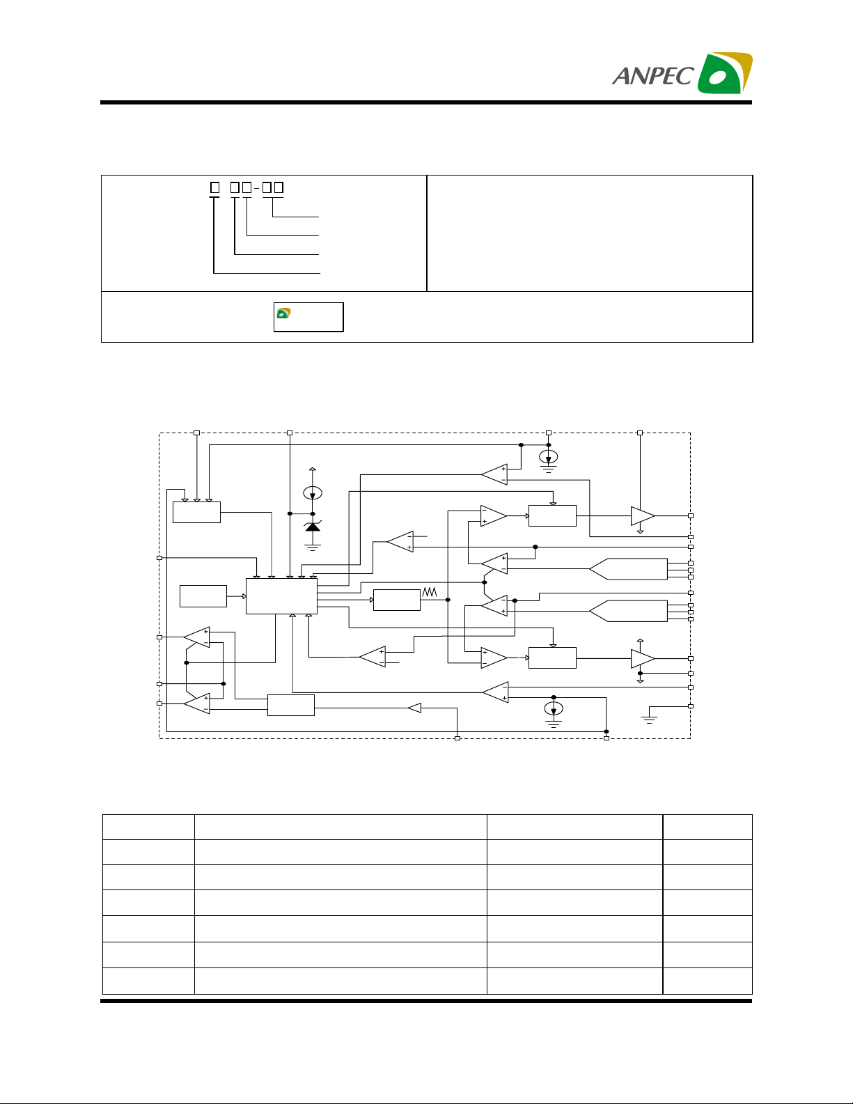
Block Diagram
VCC SS OCSET1 BOOT
Power On
Reset
SD
Therm al
Protection
SOURCE
INHIBIT
FB
SINK
50%
APW 7046
XXXXX
S oft- S tart an d
Fault Logic
Resistor
Divider
Handling Code
Tem p. Range
Package C ode
Voltage Code
VCC
28µ A
4.5V
OVP2
OVP1
O s c illa to r
115%
MEM
V
115%
Vcore
B u ffe r
Voltage Code
A : V CO RE ( 1.1 5 ~ 1 .5 0 V ) V M EM(2 .4 0 ~ 2 .75 V)
B : V CO RE ( 1.1 5 ~ 1 .5 0 V ) V M EM(2 .8 0 ~ 3 .15 V)
Package C ode
K : S OP - 24
Tem p. Range
C : 0 to 7 0
C
°
Handling Code
TU : T u b e TR : T a p e & Re e l
XXXXX - Date Code
INHIBIT
Gate
Control
INHIBIT
Gate
Control
200µ A
CORE
V
MEM
V
TTL D/A
Converter
TTL D/A
Converter
BOO T
OC1
PW M1
EA1
EA2
PW M2
OC2
200uA
UGATE1
PHASE1
VSEN1
CORE0
CORE1
CORE2
VSEN2
MEM0
MEM1
MEM2
UGATE2
PGND
PHASE2
GND
VIN
OCSET2
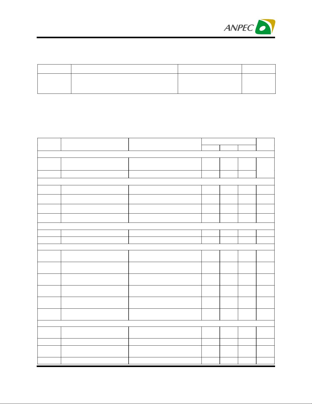
Absolute Maximum Ratings
Symbol Parameter Rating Unit
V
CC
VI , V
T
A
T
J
T
STG
T
S
Copyright ANPEC Electronics Corp. Rev. A.
Rev.A.2 - Mar., 2002
Supply Voltage 15 V
Input , Output or I/O V oltage GND -0.3 V to VCC +0.3 V
O
Operating Ambient Temperature Range 0 to 70
Junction Temperature Range 0 to 125
Storage Temperature Range -65 to +150
Soldering Temperature 300 ,10 seconds
www.anpec.com.tw2
C
°
C
°
C
°
C
°
APW7046
Thermal Characteristics
Symbol Parameter Value Unit
R
JA
Electrical Characteristics
Unless otherwise specified, these specifications apply over VCC=VBOOT=12V and TA=0~70°C.
Typical values refer to TA=25°C.
Thermal Resistance in Free Air
SOIC
SOIC (with 3in
2
of Copper)
75
65
C/W
°
Symbol Parameter Test Conditions
Supply Current
I
I
CCSD
Nominal Supply Current
CC
Shutdown Su pply Current SD=5V 2.7
S D=0 V, UGAT E1 ,UGATE2
, SOUR C E , and SINK O p en
Power-on Reset
Rising VCC Threshold Vocset=3V 4.2 4.6 V
Fa llin g V CC Thr e s h o ld Voc s et = 3 V 3.6 V
SD In p u t H ig h Voltag e 2.0 V
SD Input Low Voltage 0.8 V
Oscillator
F
V
∆
Free Running Frequency 185 200 215 kHz
OSC
Ramp Amplitude 1.9 V
OSC
PW M Co ntroller Reference Voltage
V
CORE
PW M 1 R eference Voltage
Accuracy
COR E0-C ORE2 Input High
Voltage
COR E0-C ORE2 Input Low
Voltage
V
PW M 2 R eference Voltage
MEM
Accuracy
M E M 0 - M E M2 In p u t H ig h
Voltage
M E M 0 - M E M2 In p u t Lo w
Voltage
SOU R C E -SINK L inear Controller
V
FB Re gulation Voltage
FB
Regulator Sourcing or Sinking
Current
VFB accuracy -25 +25 mV
Max. SOURCE Pin Drive
Current
Max. SINK Pin Drive C u rrent
APW 7046
Min. Typ. Max.
8
Unit
mA
-1 +1 %
2.0 V
0.8 V
-1.5 +1.5 %
2.0 V
0.8 V
0.5VIN V
0.8
±
0.8
±
mA
mA
Copyright ANPEC Electronics Corp. Rev. A.
Rev.A.2 - Mar., 2002
www.anpec.com.tw3
APW7046
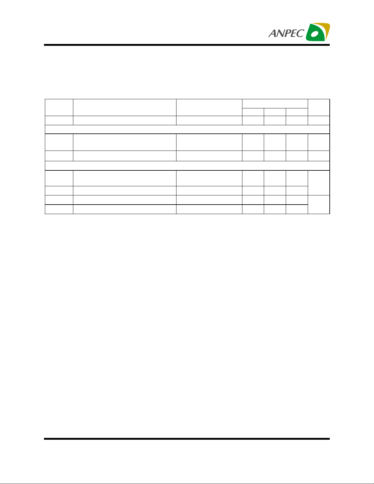
Electrical Characteristics (Cont.)
Unless otherwise specified, these specifications apply over VCC=VBOOT=12V and TA=0~70°C.
Typical values refer to TA=25°C.
Symbol Parameter Test Conditions
I
VIN Input Bias Current VIN=2.5V 2 uA
VIN
PWM Controllers Gate Drivers
I
UGATE
R
GATE
V
UGATE1,2 Source
CC=VBOOT
V
UGATE1,2
UGATE Sink VCC=12V,V
=12V,
=6V
UGATE1,2
Protection
VSEN1,2 OVP trip point
(VSEN1/V
and VSEN 2/V
CORE
MEM
VSEN Rising 115 120
)
VSEN1,2 O.V. Hysteresis 2
I
OCSET
I
Ocset Current Source Vocset=3V 170 200 230
Soft start Current 28
SS
Functional Pin Description
VCC (Pin 1)
Provide a +12V bias supply for the IC to this pin. This
pin also provides the gate bias charge for the
MOSFETs of the SOURCE-SINK regulator. The voltage at this pin is monitored for Power-On Reset (POR)
purposes.
UGA TE1 (Pin 2)
Connect this pin to the MOSFET gate of the PWM1
converter. This pin provides the gate drive for the
MOSFET.
sets the soft-start interval of all power controls and
preventing the outputs from overshoot as well as limiting the input current .
SD (Pin 5)
The pin shuts down all power outputs. A TTL compatible , logic level high signal applied at this pin immediately discharges the soft-start capacitor,disabling all
power outputs. When re-enabled, the IC undergoes a
new soft-start cycle. Left open, this pin is pulled low
by an internal pull-down resistor, enabling operation.
APW7046
Min. Typ. Max.
0.74 A
=6V 3 4
Unit
Ω
%
uA
PHASE1 (Pin 3)
Connect this pin to the PWM1 converter’s MOSFET
source.This pin is used to monitor the voltage drop
across the MOSFET for over-current protection.
SS (Pin 4)
Connect a capacitor from this pin to ground.This
capacitor, along with an internal 28uA current source,
Copyright ANPEC Electronics Corp. Rev. A.
Rev.A.2 - Mar., 2002
SOURCE (Pin 6)
Connect this pin to the upper MOSFET gate drive of
the SOURCE-SINK regulator. This pin drives the upper external MOSFET as a sourcing regulator.
SINK (Pin 7)
Connect this pin to the lower MOSFET gate drive of
www.anpec.com.tw4

APW7046
Functional Pin Description (Cont.)
the SOURCE-SINK regulator. This pin drives the lower
external MOSFET as a sinking regulator.
FB (Pin 8)
Connect this pin to output of the SOURCE-SINK
regulator. This pin provides the voltage feedback path
for the sourcing and sinking regulators. This pin is internally connected to the negative input of the SOURCE
controller, and also connected to the positive input of
the SINK controller.
VIN (Pin 9)
Connect this pin to VMEM or a fixed voltage source.
Two voltages, about 0.5VIN, are generated by an internal resistor divider as the reference voltages of the sourcing and sinking regulators. The sinking regulation voltage is higher than the sourcing one to prevent a direct
current path through the upper and lower MOSFETs.
OCSET1 (Pin 10)
Connect a resistor (R
the PWM1 converter’s MOSFET. R
200uA current source (I
resistance(r
) set the converter’s over-current (OC)
DS(ON)
) from this pin to the drain of
OCSET
, an internal
OCSET
), and the MOSFET’s on-
OCSET
trip point according to the following equation:
I
PEAK
=
OCSET
r
OCSET
DS( ON)
I
x R
An over-current trip cycles the soft-start function. The
voltage at this pin is monitored for Power-On Reset
(POR) purposes.
VSEN1 (Pin 11)
This pin is connected to the PWM1 converter’s output
voltage to provide the voltage feedback path. The overvoltage protection(OVP) comparator uses this pin to
monitor the output voltage for over- voltage protection
GND (Pin 12)
Signal ground for the IC. All voltage levels are measured with respect to this pin.
VSEN2 (Pin 13)
This pin is connected to the PWM2 converter’s output
voltage to provide the voltage feedback path. The overvoltage protection(OVP) comparator uses this pin to
monitor the output voltage for over- voltage protection.
OCSET2 (Pin 14)
Connect a resistor (R
the PWM2 converter’s MOSFET. The function of this pin is
similar to OCSET1(pin 10) for OC detection and POR
purposes.
) from this pin to the drain of
OCSET
CORE0-2 (Pin 15-17)
CORE0-2 are TTL-compatible logic level input pins to
the 3-bit DAC. The states of the three pins set the
internal reference voltage (VCORE) for the PWM1 converter and also set the OVP threshold voltage for
PWM1 converter.
MEM0-2 (Pin 18-20)
MEM0-2 are TTL-compatible logic level input pins to
the other 3-bit DAC. The states of the three pins set
the internal reference voltage (VMEM) for the PWM2
converter and also set the OVP threshold voltage for
PWM2 converter.
PGND (Pin 21)
Connect this pin to the anode of the flywheel diodes
of the two PWM converters.
PHASE2 (Pin 22)
Connect this pin to the PWM2 converter’s MOSFET
source.This pin is used to monitor the voltage drop
across the MOSFET for over-current protection.
Copyright ANPEC Electronics Corp. Rev. A.
Rev.A.2 - Mar., 2002
www.anpec.com.tw5

APW7046
Functional Pin Description
UGA TE2 (Pin 23)
Connect this pin to the MOSFET gate of the PWM2
converter. This pin provides the gate drive for the
MOSFET.
Table 1 DAC Table
APW7046 - A
Pin Name
CORE2 CORE1 CORE0
V
CORE
Voltage
0 0 0 1.15
0 0 1 1.20
0 1 0 1.25
0 1 1 1.30
1 0 0 1.35
1 0 1 1.40
1 1 0 1.45
1 1 1 1.50
Pin Name
MEM2 MEM1 MEM0
V
MEM
Voltage
0 0 0 2.40
0 0 1 2.45
0 1 0 2.50
0 1 1 2.55
1 0 0 2.60
1 0 1 2.65
1 1 0 2.70
1 1 1 2.75
BOOT (Pin 24)
Connect this pin to +12V. This pin provides bias voltage to the MOSFET drivers.
APW7046 - B
Pin Name
CORE2 CORE1 CORE0
V
CORE
Voltage
0 0 0 1.15
0 0 1 1.20
0 1 0 1.25
0 1 1 1.30
1 0 0 1.35
1 0 1 1.40
1 1 0 1.45
1 1 1 1.50
Pin Name
MEM2 MEM1 MEM0
V
MEM
Voltage
0 0 0 2.80
0 0 1 2.85
0 1 0 2.90
0 1 1 2.95
1 0 0 3.00
1 0 1 3.05
1 1 0 3.10
1 1 1 3.15
Copyright ANPEC Electronics Corp. Rev. A.
Rev.A.2 - Mar., 2002
www.anpec.com.tw6

APW7046
Simplified Power System Diagram
+5V
Q2
Standard Buck
VMEM
Converter
(PWM2)
Q3
VTT
SOURCE-SINK
Linear Converter
Q4
Typical Application Circuit
+12V
+3.3V
VCORE
VMEM
VTT
C5
10uF
330uF
L1
1uH
C4
330uF
C3
10uF
L2
4.7uH
R4
C7
C6
330uF
3
Q1
APM9410
R5
R1
10
C2
200pF
R2
1.5K
R3
5.1
D1
MBRD835L
1K
R6
10K
C8
330uF
R7
NC
C9
0.1uF
Q3
APM3055
C10
330uF
Q4
APM3055
10
11
2
3
9
6
7
8
C1
1uF
1
VCC
OCSET 1
UGATE1
PHASE1
VSEN1
VIN
SOURCE
SINK
FB
APW7046
Standard Buck
Converter
(PWM1)
24
BOOT
14
OCSET 2
23
UGATE2
PHASE2
21
PGND
13
VSEN2
20
MEM2
19
MEM1
18
MEM0
17
CORE2
16
CORE1
15
CORE0
5
EN
4
SS
GND
12
C2
1uF
C11
200pF
R8
1.5K
R9
5.1
C16
0.68uF
Q1
Q2
APM9410
D2
MBRD835L
MEM2
MEM1
MEM0
CORE2
CORE1
CORE0
C12
10uF
L4
7.8uH
C13
330uF
R10
0
R11
NC
+3.3V
VCORE
L3
1uH
+5V
C14
10uF
VMEM
C15
330uF
C4, C6, C7, C8 , C10, C13, C15 : 330uF/6.3V
SMD Low ESR tantalum Capacitor
Copyright ANPEC Electronics Corp. Rev. A.
Rev.A.2 - Mar., 2002
www.anpec.com.tw7

APW7046
Typical Performance
1. SOURCE-SINK Linear Regulator Transient Response
- The output capacitor is 330uF (Low ESR tantalum capacitor)
- Define the output cerrent (IVTT) sourcing from the regulator to be positive.
- The interval of current transitions in figures 1 and 2 are all smaller than 1uS.
- In figure 1, the IVTT transition is from -0.2A to 4A.
- In figure 2, the IVTT transition is from 0.2A to -4A.
Figure 1 Figure 2
Copyright ANPEC Electronics Corp. Rev. A.
Rev.A.2 - Mar., 2002
www.anpec.com.tw8

APW7046
Packaging Information
SO – 300mil ( Reference JEDEC Registration MS-013)
D
N
EH
12
3
GAUGE
PLANE
A
e
B
A1
Millimeters Variations- D Inches Variations- D
Dim
Min. Max. Variations Min. Max.
A2.35
0.10 0.30
A1
0.33 0.51
B
2.65
SO-16
SO-18
SO-20
D See variations SO-24
7.40 7.60
E
SO-28
e 1.27BSC SO-14
H
L
10 10.65
0.40 1.27
10.10 10.50
11.35 11.76
12.60 13
15.20 15.60
17.70 18.11
8.80 9.20
Dim
Min. Max.
A 0.093 0.1043 SO-16 0.398 0.413
A1 0.004 0.0120 SO-18 0.447 0.463
B 0.013 0.020 SO-20 0.496 0.512
D See variations SO-24 0.599 0.614
E 0.2914 0.2992 SO-28 0.697 0.713
e 0.050BSC SO-14 0.347 0.362
H0.3940.419
L0.0160.050
N See variations N See variations
10°8
φ
°φ
10°8
°
Variation
L
1
Min. Max.
Copyright ANPEC Electronics Corp. Rev. A.
Rev.A.2 - Mar., 2002
www.anpec.com.tw9

APW7046
Physical Specifications
Terminal Material Solder-Plated Copper (Solder Material : 90/10 or 63/37 SnPb)
Lead Solderability Meets EIA Specification RSI86-91, ANSI/J-STD-002 Category 3.
Packaging 1000 devices per reel for SOP-24.
Reflow Condition (IR/Convection or VPR Reflow)
Reference JEDEC Standard J-STD-020A APRIL 1999
Peak temperature
temperature
Pre-heat temperature
°
183 C
Time
Classificatio n R e flow Profiles
Convection or IR/
Convection
Average ramp-up rate(183°C to Peak) 3°C/second max. 10 °C /second max.
Preheat temperature 125 ± 25°C)
Temperature maintained above 183°C
Time within 5°C of actual peak temperature
Peak temperature range
Ramp-down rate
Time 25°C to peak temperature
120 seconds max
60 – 150 seconds
10 –20 seconds 60 seconds
220 +5/-0°C or 235 +5/-0°C 215-219°C or 235 +5/-0°C
6 °C /second max. 10 °C /second max.
6 minutes max.
VPR
Package Reflow Conditions
pkg. thickness ≥≥≥≥ 2.5mm
and all bgas
Convection 220 +5/-0 °C Convection 235 +5/-0 °C
VPR 215-219 °C VPR 235 +5/-0 °C
IR/Convection 220 +5/-0 °C IR/Convection 235 +5/-0 °C
Copyright ANPEC Electronics Corp. Rev. A.
Rev.A.2 - Mar., 2002
pkg. thickness < 2.5mm and
pkg. volume ≥≥≥≥ 350 mm³
pkg. thickness < 2.5mm and p kg .
volume < 350mm³
www.anpec.com.tw10

APW7046
Re lia bility test p r o gram
Test item Method Description
SOLDERABILITY MIL-STD-883D-2003
HOLT MIL-STD-883D-1005.7
PCT JESD-22-B, A102
TST MIL-STD-883D-1011.9
ESD MIL-STD-883D-3015.7 VHBM > 2KV, VMM > 200V
Latch-U p JESD 78 10ms , Itr > 100mA
Carrier Tape & Reel Dimensions
245°C , 5 SEC
1000 Hrs Bias @ 125 °C
168 Hrs, 100 % RH , 121°C
-65°C ~ 150°C, 200 Cycles
t
W
E
F
Po
A
P
P1
Ao
J
D
Bo
D1
T2
C
B
T1
Ko
Application
SOP- 24
Copyright ANPEC Electronics Corp. Rev. A.
Rev.A.2 - Mar., 2002
ABCJT1T2WPE
330±162 ±1.5
F D D1 Po P1 Ao Bo Ko t
11.5 ± 0.1 1.55 +0.1 1.5+ 0.25 4.0 ± 0.1 2.0 ± 0.1 10.9 ± 0.1 15.9± 0.1 3.1± 0.1 0.35±0.05
12.75
0.15
±
2 ± 0.6 24.4 ± 0.2 2± 0.2 24 ± 0.3 12 ± 0.1 1.75± 0.1
www.anpec.com.tw11

APW7046
Cover Tape Dimensions
Application Carrier Width Cover Tape Width
SOP- 16 / 20 / 2 4 / 2 8
Customer Service
Anpec Electronics Corp.
Head Office :
5F, No. 2 Li-Hsin Road, SBIP,
Hsin-Chu, T aiwan, R.O.C.
T el : 886-3-5642000
Fax : 886-3-5642050
Taipei Branch :
7F, No. 137, Lane 235, Pac Chiao Rd.,
Hsin Tien City, Taipei Hsien, Taiwan, R. O. C.
T el : 886-2-89191368
Fax : 886-2-89191369
24 21.3
Copyright ANPEC Electronics Corp. Rev. A.
Rev.A.2 - Mar., 2002
www.anpec.com.tw12
 Loading...