ANPEC APW7025KC-TU, APW7025KC-TR Datasheet

APW7025
Advanced PWM and Dual Linear Power Control
Features General Description
••
•
3 Regulated Voltage are provided
••
••
• Switching Power for VTT(1.25V)
••
••
• Linear1 Regulator for FBVDDQ(2.5V)
••
••
• Linear2 Regulator for NVVDD(2.05V)
••
••
•
Simple Single-Loop Control Design
••
••
• Voltage-Mode PWM Control
••
••
• Excellent Output Voltage Regulation
••
••
• PWM Output: ±1%
••
••
• Linear Output: ±3%
••
••
• Fast Transient Response
••
••
• High-Bandwidth Error Amplifier
••
••
• Full 0% to 100% Duty Ratio
••
••
• Power-Good Output Voltage Monitor
••
••
• Over-Voltage and Over-Current Fault Monitors
••
••
• Small Converter Size
••
••
• Constant Frequency Operation(200kHz)
••
••
• Programmable Oscillator from 50kHz to 1MHz
••
••
• Reduce External Component Count
••
The APW7025 integrates a PWM controller and Dual
linear controller, as well as the monitoring and protection functions into a single package , which provides three controlled power outputs with over-voltage and over-current protections. The PWM controller regulates the DDR reference voltage with a synchronous-rectified buck converter. The linear controller regulates power for microprocessor core voltage
and Memory Voltage.
The precision reference and voltage-mode PWM
control provide ±2% static regulation. The linear
controller drives an external N-channel MOSFET to
provide adjustable voltage.
The APW7025 monitors all the output voltages , and
a single Power Good signal is issued when the PWM
Voltage is within 10% of the 1.25V setting and the
other output levels are above their under-voltage
thresholds. Additional built-in over-voltage protection for the PWM output uses the lower MOSFET to
prevent output voltages above 115% of the 1.25V
setting. The PWM over-current function monitors
the output current by using the voltage drop across
the upper MOSFET’s R
, eliminating the need
DS(ON)
for a current sensing resistor.
Pin Description
Applications
VCC
••
• Motherboard Power Regulation for Computers
••
••
• Low-Voltage Distributed Power Supplies
••
••
• VGA Card Power Regulation
••
ANPEC reserves the right to make changes to improve reliability or manufacturability without notice, and advise
customers to obtain the latest version of relevant information to verify before placing orders.
Copyright ANPEC Electronics Corp.
Rev.P.1 - Mar., 2001
DRIVE2
PGOOD
VSEN2
FAULT
NC
NC
NC
NC
NC
SS
NC
1
2
3
4
5
6
7
8
9
10
11
12
24
23
22
21
20
19
18
17
16
15
14
13
UGATE
PHASE
LGATE
PGND
OCSET
VSEN1
FB
COMP
VSEN3
DRIVE3
GND
VAUX
SOP24
www.anpec.com.tw1

APW7025
Ordering Information
APW7025
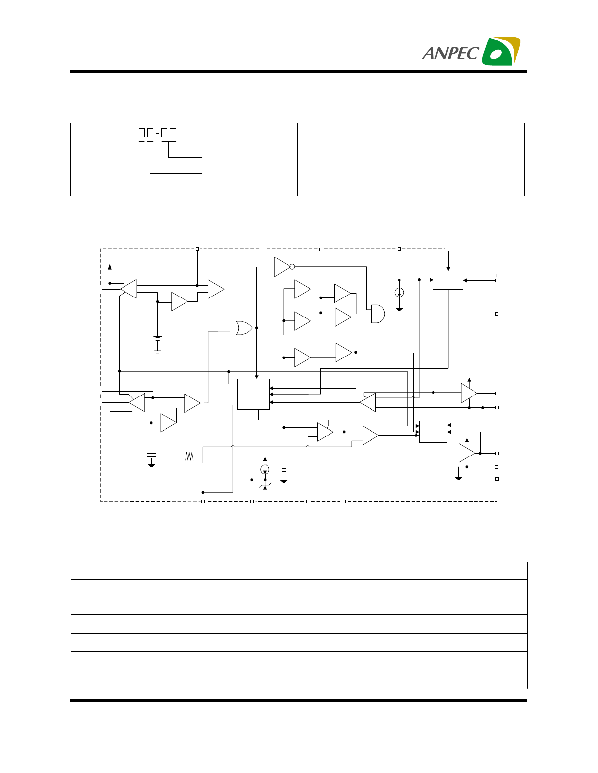
Block Diagram
VAUX
DRIVE3
VSEN2
DRIVE2
-
1.5V
+
+
1.26V
-
+
+
-
×
0.75
Handling Code
Temp. Range
Package Code
VSEN3
-
+
-
+
OSCILLATOR
INHIBIT
FAULT
LUV
LINEAR
UNDER-
VOLTAGE
START &
SOFT
FAULT
LOGIC
Package Code
K : SOP - 24
Temp. Range
C : 0 to 70 C
°
Handling Code
TU : Tube TR : Tape & Reel
INHIBIT
CONTROL
GATE
VCC
Power-on
Reset
(POR)
DRIVER1
SYNCH
DRIVE
VAUX
PGOOD
VCC
UGATE
PHASE
V
CC
LGATE
PGND
GND
OCSETVSEN1
×
1.10
+
-
×
0.90
×
1.15
OV
ERROR
AMP1
V
CC
+
1.25V
-
µ
28
A
4.5V
+
-
+
-
+
-
OC1
200µA
+
-
+
-
PWM
COMP1
PWM1
FAULT
SS
COMPFB
Absolute Maximum Ratings
Symbol Parameter Rating Unit
V
CC
VI , V
T
A
T
J
T
STG
T
S
Copyright ANPEC Electronics Corp.
Rev. P.1 - Mar., 2001
Supply Voltage 15 V
Input , Output or I/O Voltage GND -0.3 V to VCC +0.3 V
O
Operating Ambient Temperature Range 0 to 70
Junction Temperature Range 0 to 125
Storage Temperature Range -65 to +150
Soldering Temperature 300 ,10 seconds
www.anpec.com.tw2
C
°
C
°
C
°
C
°
 Loading...