ANPEC APW7004KC-TU, APW7004KC-TR Datasheet

APW7004
Synchronous-Rectifier PWM Controller for PentiumTM II Microprocessor
Features
••
•
Simple Single-Loop Control Design-Voltage-
••
Mode PWM Control
••
•
Fast Transient Response
••
• High-Bandwidth Error Amplifier
••
•
5-Bit Digital-to-Analog Output Voltage Selec-
••
tion
TM
6´ 86
Alpha
is a trademark of Cyrix Corporation
TM
is a trademark of Digital Equipment
Corporation
TM
K6
is a trademark of Advanced Micro Devices,
Inc.
Pentium
TM
is a trademark of Intel Corporation
PowerPC
TM
is a trademark of IBM
• Wide Range from1.3VDC to 3.5V
• 0.1V Binary Steps from 2.1VDC to 3.5V
.05V Binary Steps from 1.3VDC to 2.05 V
••
• VID0-4 Input Pins with Pull High Resistors Built
••
DC
DC
DC
in
••
• Power-Good Output Voltage Monitor, PGOOD
••
Pin with an Open Collector Configuration
••
• Over-Voltage and Over-Current Fault Monitors
••
• Uses MOSFET’s R
as Current Sensing,
DS(ON)
No Extra Element Required
••
• Programmable Switching Frequency Setting
••
• 200kHz Free-Running Oscillator
Applications
••
• Power Supply for Pentium
••
Pentium
Alpha
••
• High-Power 5V to 3.xV (or below) DC-DC Regu-
••
TM
II,PowerPC
TM
Microprocessors
lators
••
• Low-Voltage Distributed Power Supplies
••
TM
, Pentium ProTM,
TM
TM
, K6
, 6´86
TM
and
General Description
The APW7004 provides a complete control and multiple protection for a DC-DC converter optimized for
high performance microprocessor applications. It is
designed to drive two N-Channel MOSFETs in a synchronous-rectified buck topology. The APW7004 integrates output voltage control, output voltage
programming, monitoring and protection functions into
a single chip IC.
The APW7004 includes a 5-bit digital-to-analog converter (DAC) that provides a easily adjustable and
precisely output voltage from 2.1VDC to 3.5V
1 increments and from 1.3 VDC to 2.05 V
05V increments. Any selected output voltage can be
maintained within ±1% accuracy over temperature
and line voltage variations.
With a 200kHz free-running triangle-wave oscillator
and a error amplifier featuring a 15MHz unity-gain
bandwidth and 6V/us slew rate inside the chip,
APW7004 can implement a simple, single feedback
loop, voltage-mode control topology with high transient performance.
The APW7004 also features with multiple protections
against over-current and over-voltage conditions by
inhibiting PWM operation. The APW7004 uses the
R
of the upper MOSFET as the current sensing
DS(ON)
element which eliminates the demend for an extra
component. The APW7004 also monitors the output
voltage using a comparator with hysteresis that tracks
the DAC output and issues a Power Good signal once
the output is within ±10%.
DC
in 0.
DC
in 0.
ANPEC reserves the right to make changes to improve reliability or manufacturability without notice, and advise
customers to obtain the latest version of relevant information to verify before placing orders.
Copyright ANPEC Electronics Corp.
Rev. P.4 - Mar., 2001
www.anpec.com.tw1

APW7004
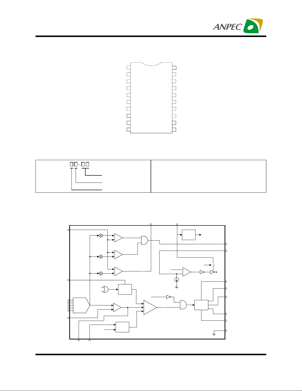
Pin Description
V
OCSET
VID0
VID1
VID2
VID3
VID4
COMP
Ordering Information
APW7004
Handling Code
Temp. Range
Package Code
Block Diagram
SEN
SS
FB
1
2
3
4
5
6
7
8
9
10
20
19
18
17
16
15
14
13
12
11
RT
OVP
V
cc
LGATE
PGND
BOOT
UGATE
PHASE
PGOOD
GND
Package Code
K : SOP - 20
Temp. Range
C : 0 to 70 C
°
Handling Code
TU : Tube TR : Tape & Reel
V
SEN
1
110%
90%
115%
OC
DETN
(Power on Reset)
DAC OUT
DETN
(Power on Reset)
RT
VID0
VID1
VID2
VID3
VID4
SS
FB
3
4
TTL D/A
5
CONVERER
6
(DAC)
7
8
10
920
COMP
Copyright ANPEC Electronics Corp.
Rev. P.4 - Mar., 2001
+
-
+
-
+
-
ERRAMP
+
-
CP2
CP2
CP2
OSC
SOFT
START
OVP
+
+
-
OVP
DETN, OC
CP4
PHASE
V
CC
1819
200µA
Power on
Reset
CP1
+
-
UGATE
DRIVER
DETN
(Power on Reset)
OC
PGOOD
12
OCSET
2
BOOT
15
UGATE
14
PHASE
13
LGATE
17
PGND
16
GND
11
www.anpec.com.tw2

APW7004
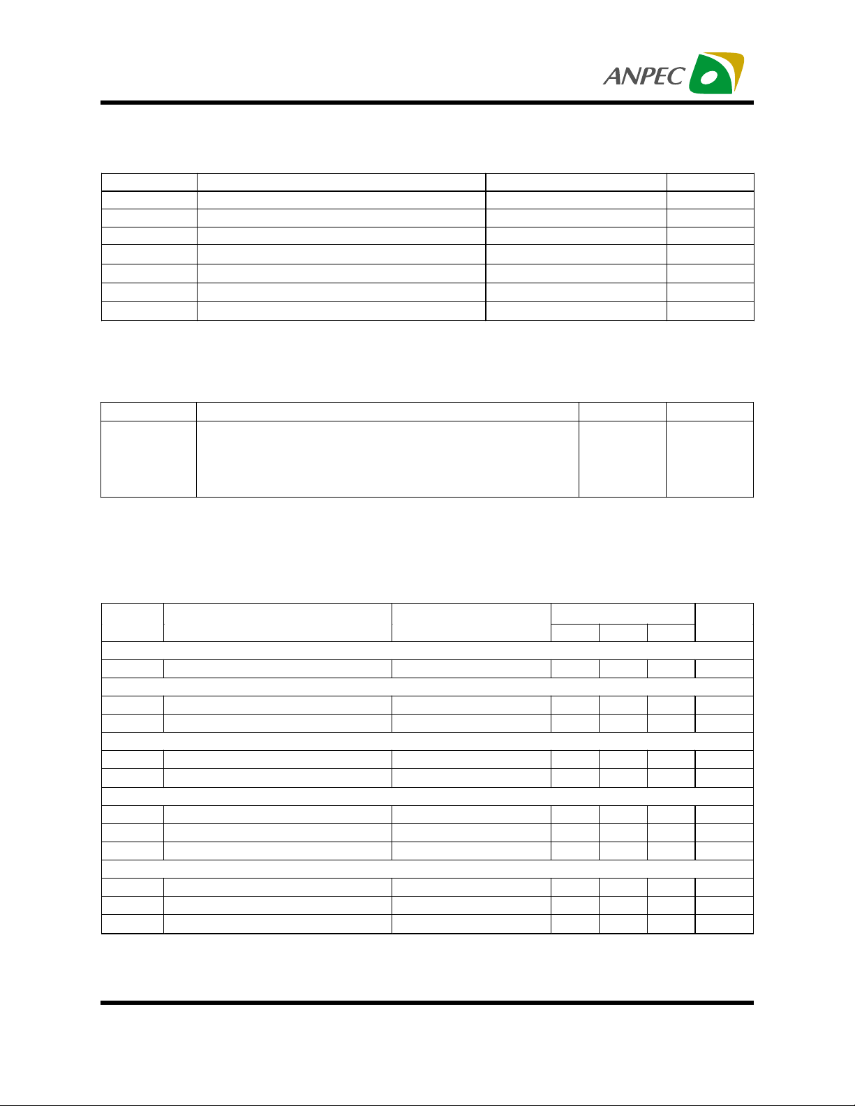
Absolute Maximum Ratings
Symbol Parameter Rating Unit
V
CC
V
–V
BOOT
,
V
V
I
T
A
T
J
T
STG
T
S
Thermal Characteristics
Symbol Parameter Value Unit
R
JA
θ
Supply Voltage 15 V
Boot Voltage 15 V
PHASE
Input , Output or I/O Voltage GND - 0.3 V to VCC + 0.3 V
O
Operating Ambient Temperature Range 0 to 70
Junction Temperature Range 0 to 150
Storage Temperature Range -65 to +150
Soldering Temperature 300,10 seconds
Thermal Resistance in Free Air
SOP
110
°C
°C
°C
°C
°C/W
SOP (with 3in2 of Copper)
86
Electrical Characteristics
Recommended operating conditions , unless otherwise noted
Symbol Parameter Test Conditions
V
Supply Current
CC
I
Nominal Supply UGA TE and LGATE open 3 mA
CC
Power-on Reset
Rising VCC Threshold Vocset=4.5V 9.0 V
Falling VCC Threshold Vocset=4.5V 8.8 V
Oscillator
Free Running Frequency RT= Open 185 200 215 kHz
Ramp Amplitude RT= Open 2 V
V
∆
OSC
Reference and DAC
DAC(VID0-VID4) Input Low Voltage 0.8 V
DAC(VID0-VID4) Input High Voltage 3.0 V
DACOUT Voltage acc ur a cy -1.0 + 1.0 %
Error Amplifier
DC Gain 88 dB
GBW Gain-Bandwidth Product 15 MHz
SR Slew Rate COMP=20pF 6
APW7004
Min. Typ. Max.
Unit
P-P
V/µs
Copyright ANPEC Electronics Corp.
Rev. P.4 - Mar., 2001
www.anpec.com.tw3
 Loading...