ANPEC APW6021AKC-TU, APW6021AKC-TR Datasheet

APW6021A
Advanced PWM and Triple Linear Power Controllers
Functional
••
•
4 Regulated Voltages are provided
••
••
• Microprocessor Core (1.3V to 3.5V)
••
••
• AGP Bus (1.5V or 3.3V)
••
••
• Memory (1.8V) / GTL Bus (1.5V)
••
••
•
Linear Controllers Drives with both MOSFET
••
and Bipolar Series Pass Transistors
••
• Fixed or Externally Resistor-Adjustable Linear
••
Outputs (FIX Pin)
••
• Voltage-Mode PWM Control
••
••
• Fast PWM Converter Transient Response
••
••
• High-Bandwidth Error Amplifier
••
••
• Full 0% to 100% Duty Ratio
••
••
• Excellent Output Voltage Regulation
••
••
• Core PWM Output: ± 1% Over Temperature
••
••
• Other Outputs: ± 3% Over Temperature
••
••
• TTL-Compatible 5- Bit DAC Microprocessor
••
Core Output Voltage Selection
••
• Shutdown Feature Removed When All Inputs
••
High
••
• Wide Range - 1.3VDC to 3.5 V
••
••
• Power-Good Output Voltage Monitor
••
••
• Over-Voltage and Over-Current Fault Monitors
••
••
• Switching Regulator Does Not Require
••
Extra Current Sensing Element, Uses Upper
MOSFET’s r
••
• Small Converter Size
••
••
• Constant Frequency Operation
••
••
• 200kHz Free-Running Oscillator; Program-
••
mable From 50kHz to Over 1MHz
DS(ON)
DC
Applications
••
•
Motherboard Power Regulation for Computers
••
General Description
The APW6021A provides the power control and protection for four output voltages in high-performance,
graphics intensive microprocessor and computer
applications. The IC integrates voltage-mode PWM
controller and three linear controllers, as well as the
monitoring and protection functions into a 28-pin SOIC
package. The synchronous-rectified buck converter
includes an Intel-compatible , TTL 5-input digital-toanalog converter (DAC)that adjusts the core PWM
output voltage from 1.3VDC to 2.05VDC in 0.05V steps
and from 2.1VDC to 3.5VDC in 0.1V increments. the
precision reference and voltage-mode control provide
±1% static regulation. A TTL-compatible signal ap-
plied to the SELECT pin dictates which method of
control is used for the AGP bus power : a low state
results in linear control of the AGP bus to 1.5V , while
a high state transitions the output through a linearly
controlled softstart to 3.3V , followed by full enhancement of the external MOSFET to pass the input
voltage. The other two linear regulators provide fixed
output voltages of 1.5V GTL bus power and 1.8V
power for the North/South Bridge core and/or cache
memory. These levels are user-adjustable by means
of an external resistor divider and pulling the FIX pin
low. All linear controllers can employ either N-Chan-
nel MOSFETs or bipolar NPNs for the pass transistor.
The APW6021A monitors all the output voltages. A
single Power Good signal is issued when the core is
within ±10% of the DAC setting and all other outputs
are above their under-voltage levels. Additional builtin over-voltage protection for the core output uses
the lower MOSFET to prevent output voltages above
115% of the DAC setting. The PWM controller’s overcurrent function monitors the output current by using
the voltage drop across the upper MOSFET’s r
DS(ON)
.
ANPEC reserves the right to make changes to improve reliability or manufacturability without notice, and advise
customers to obtain the latest version of relevant information to verify before placing orders.
Copyright ANPEC Electronics Corp.
Rev. A.1 - Mar., 2001
www.anpec.com.tw1

APW6021A
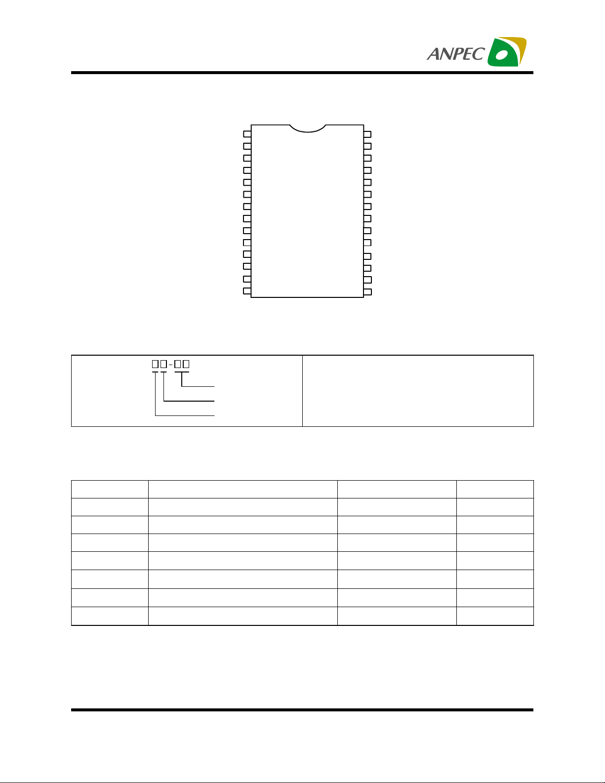
Pin Description
DRIVE2
FIX
VID4
VID3
VID2
VID1
VID0
PGOOD
SD
VSEN2
SELECT
SS
FAULT/ RT
VSEN4
Ordering Information
APW6021A
Handling Code
Temp. Range
Package Code
13
14
1
2
3
4
5
6
7
8
9
10
11
12
28
27
26
25
24
23
22
21
20
19
18
17
16
15
Package Code
K : SOP - 28
Temp. Range
C : 0 to 70 C
Handling Code
TU : Tube TR : Tape & Reel
VCC
UGATE
PHASE
LGATE
PGND
OCSET
VSEN1
FB
COMP
VSEN3
DRIVE3
GND
VAUX
DRIVE4
°
Absolute Maximum Ratings
Symbol Parameter Rating Unit
V
CC
V
–V
BOOT
Copyright ANPEC Electronics Corp.
Rev. A.1 - Mar., 2001
VI , V
T
T
T
STG
T
PHASE
O
A
J
S
Supply Voltage 15 V
Boot Voltage 15 V
Input , Output or I/O Voltage GND -0.3 V to VCC +0.3 V
Operating Ambient Temperature Range 0 to 70
Junction Temperature Range 0 to 125
Storage Temperature Range -65 to +150
Soldering Temperature 300 ,10 seconds
C
°
C
°
C
°
C
°
www.anpec.com.tw2

APW6021A
Thermal Characteristics
Symbol Parameter Value Unit
Thermal Resistance in Free Air
R
JA
θ
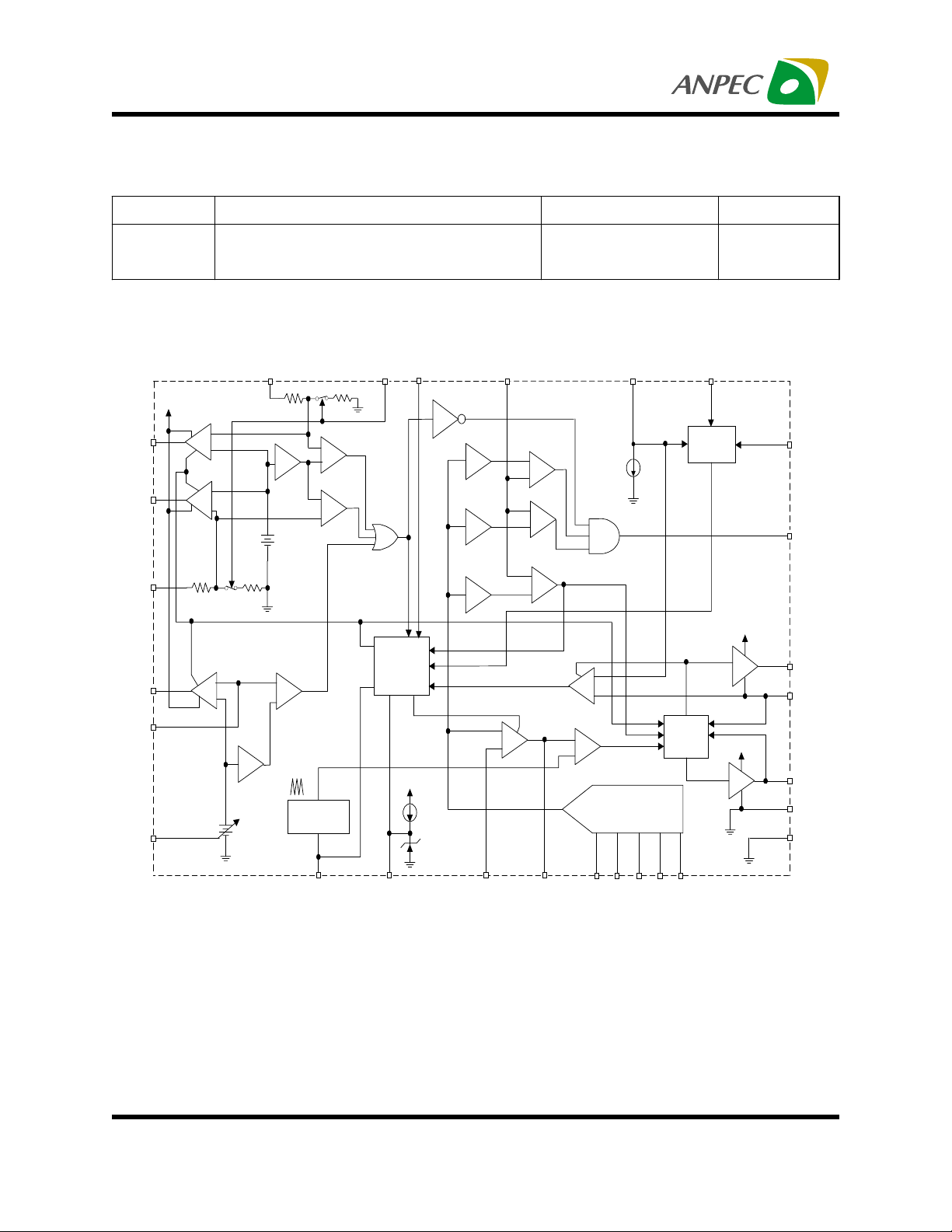
Block Diagram
SOIC
SOIC (with 3in
2
of Copper)
75
65
C/W
°
DRIVE3
DRIVE 4
VSEN 4
DRIVE2
VSEN2
SELECT
VAUX
INHIBIT
GATE
CONTROL
VCC
Power-on
Reset
(POR)
DRIVER1
SYNCH
DRIVE
VAUX
PGOOD
VCC
UGATE
PHASE
VCC
LGATE
PGND
GND
+
-
+
-
PWM
COMP1
OCSETVSEN1
200µA
PWM1
TTL D/A
CONVERTER
(DAC)
SDFIXVSEN3
+
+
-
+
-
+
×
0.75
1.5V
+
or
-
3.3v
×
0.75
1.26V
+
-
OSCILLATOR
+
+
-
VOLTAGE
INHIBIT
FAULT
LUV
LINEAR
UNDER-
SOFT START
& FAULT
LOGIC
VCC
28µA
4.5V
OV
×
×
ERROR
AMP1
DACOUT
×
1.10
0.90
1.15
+
-
+
-
+
-
OC1
+
-
FAULT/ RT
Copyright ANPEC Electronics Corp.
Rev. A.1 - Mar., 2001
VID1 VID2 VID3 VID4
COMPFBSS
VID0
www.anpec.com.tw3

APW6021A
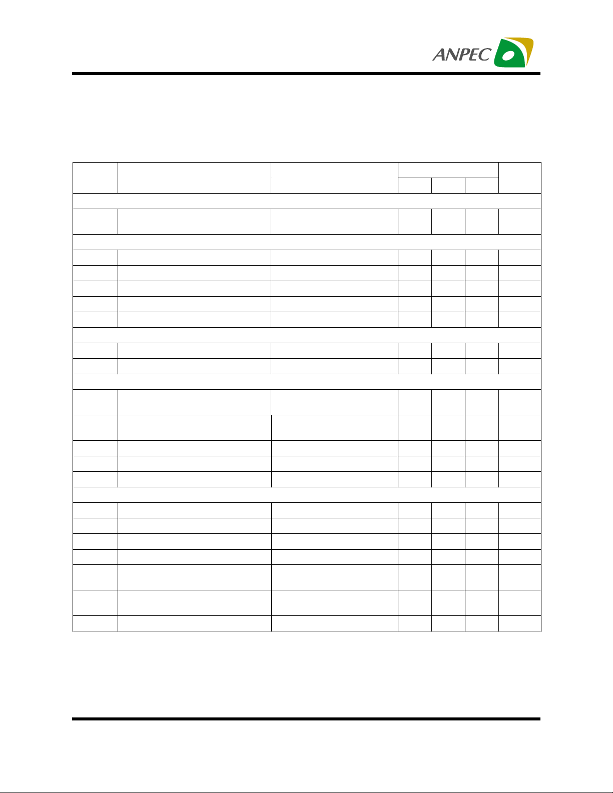
Electrical Characteristics
(Recommended operating conditions, Unless otherwise noted) Refer to Block and Simplified Power
System Diagrams, and Typical Application Schematic
APW6021A
Symbol Parameter Test Conditions
Min. Typ. Max.
VCC Supply Current
I
Nominal Supply Current
CC
UGATE, LGATE, DRIVE2,
DRIVE3, and DRIVE4 open
9mA
Power-on Reset
Rising VCC Threshold Vocset=4.5V 10.4 V
Falling VCC Threshold Vocset=4.5V 8.2 V
Rising VAUX Threshold Vocset=4.5V 2.5 V
VAUX Threshold Hysteresis Vocset=4.5V 0.5 V
Rising V
Threshold 1.26 V
OCSET
Oscillator
F
V
∆
Free Running Frequency RT= Open 185 200 215 kHz
OCS
Ramp Amplitude RT= Open 1.9 V
OSC
DAC and Bandgap Reference
DAC(VID0-VID4) Input Low
Voltage
DAC(VID0-VID4) Input High
Voltage
2.0 0.8 V
0.8 V
DACOUT Voltage accuracy -1.0 +1.0 %
V
Bandgap Reference Voltage 1.265 V
BG
Bandgap Reference Tolerance -2.5 +2.5 %
Linear Regulators (OUT2, OUT3, and OUT4)
Regulation (All Linears) 3 %
VREG2VSEN2 Regulation Voltage Select < 0.8V 1.5 V
VREG3VSEN3 Regulation Voltage 1.5 V
VREG4VSEN4 Regulation Voltage 1.8 V
VREN
Under-Voltage Level (VSEN/
UV
VREG)
Under-Voltage Hysteresis (VSEN/
VREG)
Output Drive Current (All Liners) VAUX-V
VSEN Rising 75 %
VSEN Falling 7 %
>0.6V 20 40 mA
DRIVE
Unit
P-P
Copyright ANPEC Electronics Corp.
Rev. A.1 - Mar., 2001
www.anpec.com.tw4
 Loading...