ANPEC APW3007-13KC-TU, APW3007-13KC-TR, APW3007-12KC-TU, APW3007-12KC-TR Datasheet

Copyright ANPEC Electronics Corp.
Rev. A.5 - Jun., 2003
APW3007
www.anpec.com.tw1
ANPEC reserves the right to make changes to improve reliability or manufacturability without notice, and advise customers to obtain
the latest version of relevant information to verify before placing orders.
Advanced Dual PWM and Dual Linear Power Controller
••
••
•
Provides 4 Regulated V oltages
−Microprocessor Core , I/O , Clock Chip and
GTL Bus
••
••
•
Simple Single-Loop Control Design
− Voltage-Mode PWM Control
••
••
•
Fast Transient Response
− High-Bandwidth Error Amplifier
− Full 0% to 100% Duty Ratio
••
••
• Excellent Output Voltage Regulation
− Core PWM Output : ±1% Over Temperature
− I/O PWM Output : ±2% Over Temperature
− Other Output : ±2.5% Over Temperature
••
••
• Power-Good Output Voltage Monitor
••
••
• Microprocessor Core Voltage Protection Against
Shorted MOSFET
••
••
• Over-Voltage and Over-Current Fault Monitors
••
••
• Small Converter Size
− Constant Frequency Operation
− 200kHz Free-Running Oscillator ;
Programmagle from 50kHz to 800kHz
Features General Description
The APW3007 provides the power control and protection for four output voltage in high-performance microprocessor and computer applications.
The APW3007 is designed to provide termination
voltage VTT(1.25V) with ±1% accuracy.
It integrates two PWM controllers , a linear regulator
and a liear controller as well as the monitoring and
protection function into a single package. One PWM
controller regulates the microprocessor core voltage
with a synchronous-rectified buck converter , while the
second PWM controller supplies the I/O 3.3V power
with a standard buck converter. The linear controller
regulates power for GTL bus and the intermal 200mA
regulator for clock driver circuits.
The APW3007 can provide in excess of 14A of output current for an on-board DC/DC converter via internal reference voltage. It can monitor all the output
voltage , and a single Power Good signal is issued
when the core is within 10% of the internal reference
voltage and the other levels are above their undervoltage levels. Additional built-in over-voltage protection for the core output uses the lower MOSFET to
prevent output voltage above 1 15% of the reference
voltage. The PWM controller’s over-current function
monitor the output current by sensing the voltage drop
across the upper MOSFET’s R
DS(ON)
, eliminating the
need for a current sensing resistor.
Applications
••
••
• Motherboard Power Regulation for Computers
••
••
• Low-Voltage Distributed Power Supplies
••
••
• VGA Card Power Regulation
••
••
• Termination Voltage

Copyright ANPEC Electronics Corp.
Rev. A.5 - Jun., 2003
APW3007
www.anpec.com.tw2
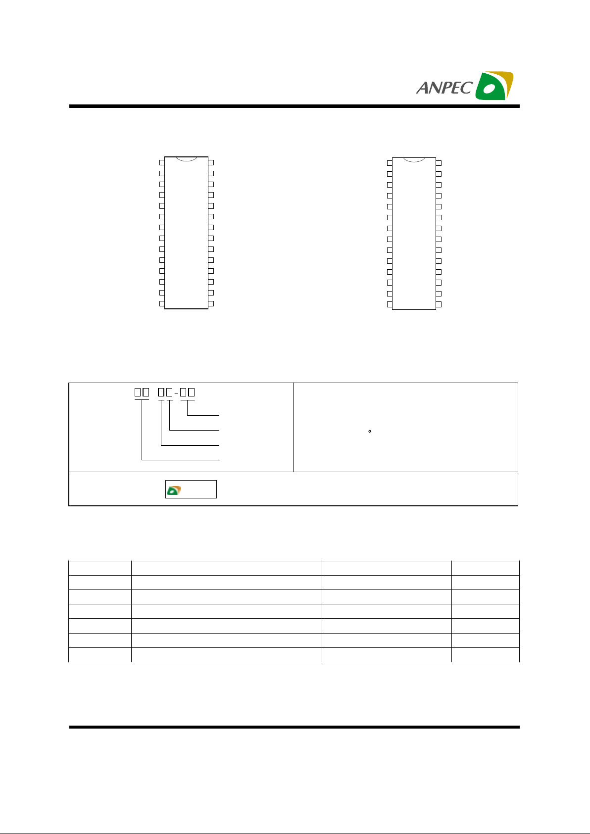
Ordering and Marking Information
Pin Description
PHASE2
NC
NC
NC
LGATE 1
OCSET1
VSEN1
NC
NC
PGOOD
V5
PGND
FB1
FB3
VSEN2
GND
1
2
3
4
5
6
7
8
12
11
10
9
24
23
22
21
NC
GATE3
PHASE1
FB2
SS
FAULT
NC
13
14
25
26
27
28
20
19
18
17
16
15
UGATE2
UGATE1
V12
OCSET2
NC
PHASE2
NC
NC
NC
LGATE 1
OCSET1
VSEN1
NC
NC
PGOOD
V5
PGND
FB1
FB3
VSEN2
GND
1
2
3
4
5
6
7
8
12
11
10
9
24
23
22
21
NC
GATE3
PHASE1
FB2
SS
FAULT
FB4
13
14
25
26
27
28
20
19
18
17
16
15
UGATE2
UGATE1
V12
OCSET2
Vout4
APW3007-12
APW3007-13
APW 3007
Voltage Code
12 : 1 .2 5 V 1 3 : 1 .3 0 V
Package C ode
K : S OP - 2 8
Tem p. Range
C : 0 to 7 0 C
Handling Code
TU : Tu b e T R : Ta p e & Reel
Handling Code
Tem p. Range
Package C ode
Voltage Code
APW 3007 K :
APW 3007
XXXXX
XXXXX - Date Code
Absolute Maximum Ratings
Symbol Parameter Rating Unit
V12 Supply Voltage 15 V
VI , V
O
Input , Output or I/O Voltage GND -0.3 V to V12 +0.3 V
T
A
Operating Ambient Temperature Range 0 to 70
°
C
T
J
Junction Temperature Range 0 to 125
°
C
T
STG
Storage Temperature Range -65 to +150
°
C
T
S
Soldering Temperature 300 ,10 seconds
°
C

Copyright ANPEC Electronics Corp.
Rev. A.5 - Jun., 2003
APW3007
www.anpec.com.tw3
Thermal Characteristics
Symbol Parameter Value Unit
R
θ
JA
Thermal Resistance in Free Air
SOIC
SOIC (with 3in
2
of Copper)
75
65
°
C/W
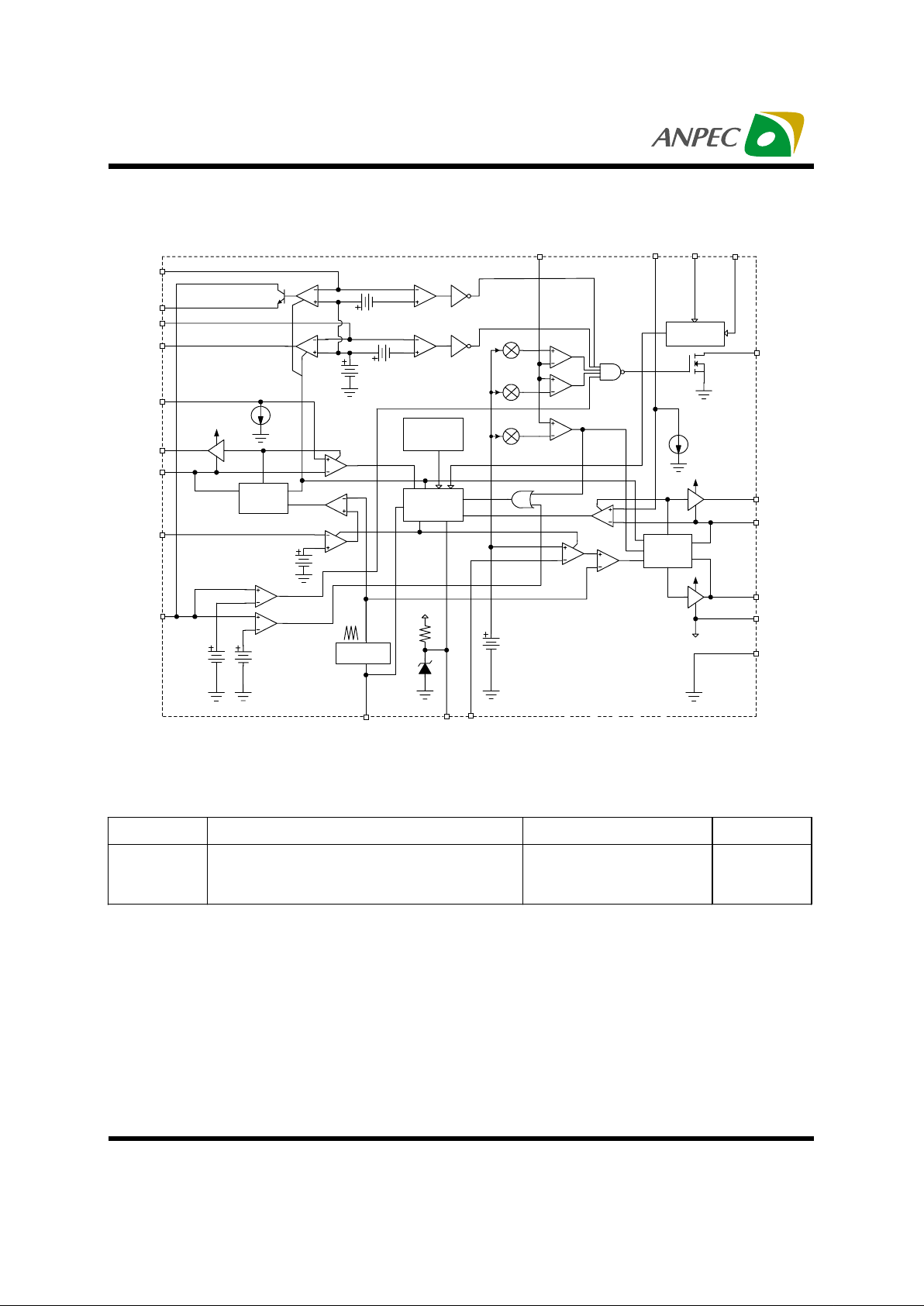
Block Diagram
GATE
CONTROL
SOFT-START
AND FAULT
LOGIC
THERMAL
PROTECTION
GATE
CONTROL
POWER-ON
RESET
FB3
GATE3
OCSET2
UGATE2
PHASE2
FB2
VSEN2
GND
PGND
LGATE1
PHASE1
UGATE1
PGOOD
V12OCSET1
FB1
SSFAULT
0.3V1.26V
200uA
VCC
DRIVE2 OC2
INHIBIT
PWM2
2.0V
ERROR
AMP2
2.5V 4.3V
V
REF
OSCILLATOR
3.3K
4.6V
ERROR
AMP1
0V
FAULT
OC1
PWM1
VCC
LOWER
DRIVE
VCC
DRIVE1
INHIBIT
115%
90%
110%
200uA
LUV
VSEN1 V5
V
OUT4
FB4
0.3V

Copyright ANPEC Electronics Corp.
Rev. A.5 - Jun., 2003
APW3007
www.anpec.com.tw4
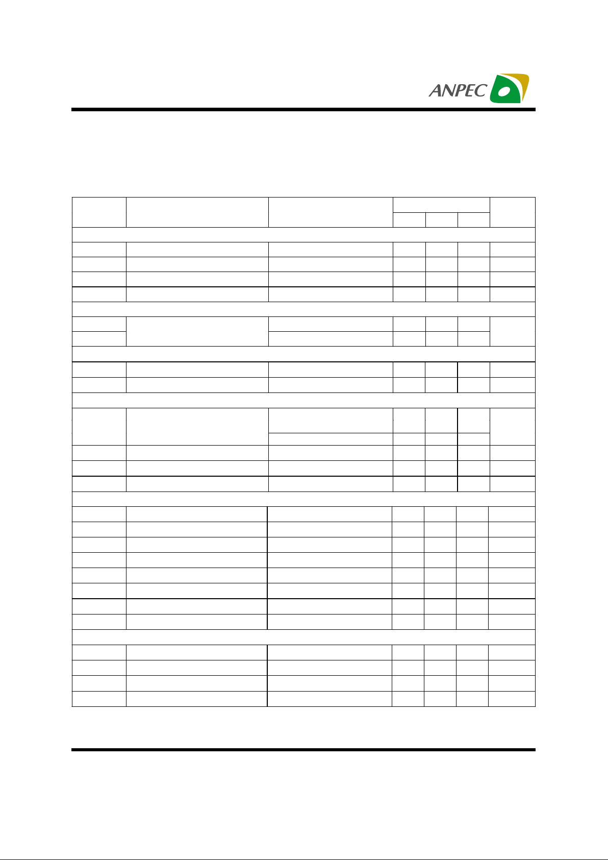
Electrical Characteristics
(Recommended operating conditions , Unless otherwise noted) Refer to Block and Simplified Power System
Diagrams , and Typical Application Schematic.
APW3007
Symbol Parameter Test Conditions
Min Typ Max
Unit
Supply UVLO Sec tion
UVLO Threshold-12 V Supply ramping up 9.5 V
UVLO Hysterises-12V 0.5 V
UVLO Threshold-5V Supply ramping up 4.3 V
UVLO Hysterises-5V 0.3 V
Supply Current
I
12
V12 6
I
5
Nominal Supply Current
V5 2
mA
Oscillator
F
OCS
Free Running Frequency RT= Open 185 200 215 kHz
∆V
OSC
Ramp Amplitude RT= Open 1.9 V
P-P
Switching Controller Reference Voltage
1.25
V
REF
Reference Voltage
APW3007-12
APW3007-13
1.30
V
Reference Voltage accuracy −1.0 +1.0 %
VFB2 Output Voltage 2 V
VFB2 Voltage Accuracy -2 +2 %
2.5V Regulator (Vout4)
Vo4 Reference Voltage TA=25 , Vout4=FB4 1.26 V
Dropout Voltage Io=200m A 0.6 V
Load Regulation 1mA<Io<200mA 0.5 %
Line Regulation 3.1V<VIO<4V , Vo=2.5V 0.2 %
Input bias Current 2 µA
Output Current 200 mA
Current Limit 300 420 mA
Thermal Shutdown 150 °C
1.5V Regulator (Vout3)
Vo3 Reference Voltage TA=25 , GATE=FB3 1.26 V
Reference Voltage Accaracy -2.5 +2.5 %
Input bias current 2 µA
Output Drive Current 50 mA
 Loading...