

ANPEC APW1681JC-TU Datasheet

APW1681
3-Channel Power Supply Supervisor
Features General Description
• Over Voltage Protection and Lock Out for
! 3.3 V, 5 V, and 12 V
• Under Voltage Protection and Lock Out for
! 3.3 V and 5 V
• Fault Protection Output with Open Drain
! Output Stage
• Open Drain Power Good Output Signal for
! Power Good Input, 3.3 V and 5 V
• 300 ms Power Good Delay
• 2.36 ms Control to Turn-Off
Delay
• 38 ms
PSON
Control Debounce
PSON
FPO
• 75 ms Delay for 3.3V and 5V Under Voltage
! Protection
• 73 µs Width Noise Deglitches
• Wide Power Supply Voltage Range
from 4 V to 15 V
• Intelligent Under Voltage Protection to Pre
vent Instantaneously AC Power Black Out
The APW1681 is designed to minimize the external components of personal-computer switching
power supply systems. It provides protection
circuits, power good indicator, fault protection output
FPO
and
PSON
control.
OVP (over voltage protection) monitors 3.3V, 5 V,
and 12 V (12 V OV detects via V
terminal). UVP
CC
(under voltage protection) monitors 3.3V and 5V.
When an OV or UV condition is detected, the PGO
(power good output) is set to low and
to high.
from low to high resets the protec-
PSON
FPO
is latched
tion latch. There is a 2.36ms turn-off delay
from
PSON
to
. There is no delay during turn
FPO
on.
Power good feature monitors PGI, 3.3V and 5V un-
der voltages, and issues a power good signal when
they are ready.
Pin Description
8
PGO
7
VCC
6
VS5
5
VS33
Applications
• PC Switching Power Supply
PGI
GND
FPO
PSON
1
2
3
4
Ordering Information
APW1681
Handling Code
Temp. Range
Package Code
ANPEC reserves the right to make changes to improve reliability or manufacturability without notice, and advise
customers to obtain the latest version of relevant information to verify before placing orders.
Copyright ANPEC Electronics Corp.
Rev. A.2 - Feb., 2001
Package Code
J : DIP - 8
Temp. Range
C : 0 to 70 C
Handling Code
TU : Tube
°
www.anpec.com.tw1
APW1681
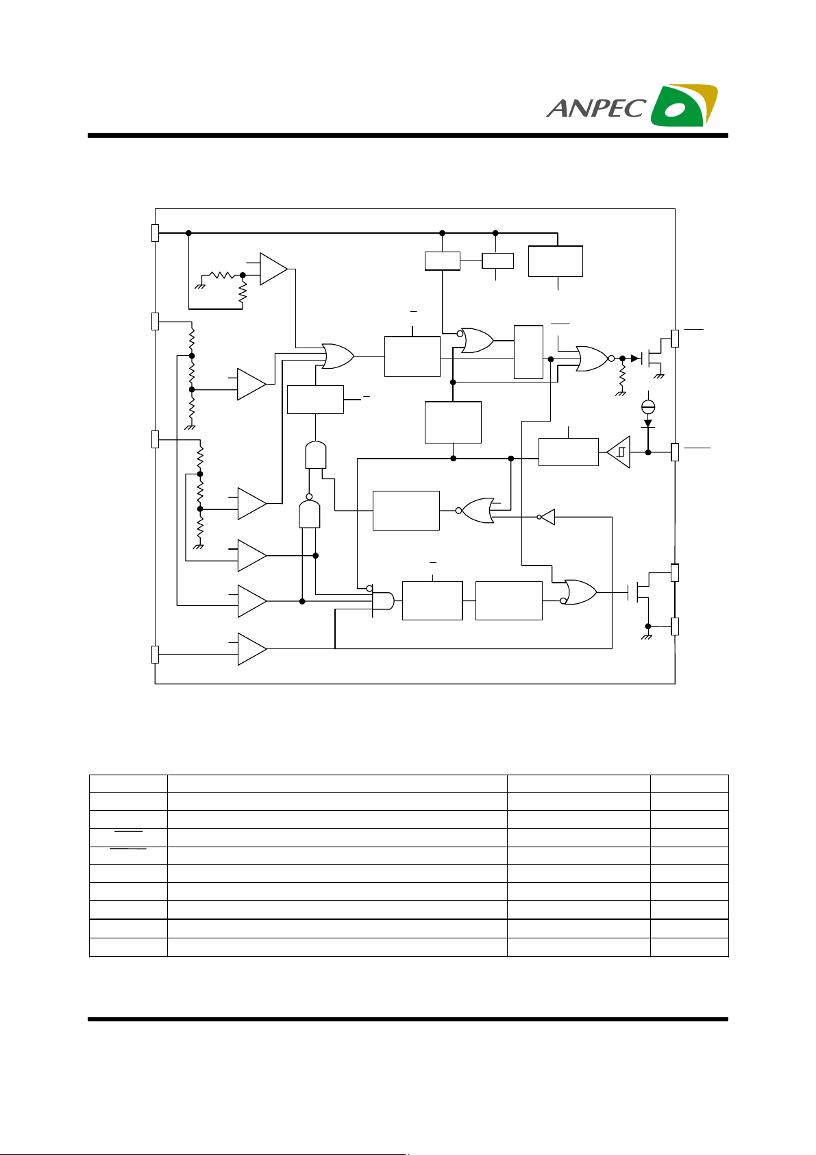
Block Diagram
V
CC
V
REF
V
S5
V
REF
RL=100k
V
S33
V
REF
RL=100k
V
REF
V
REF
V
PGI
REF
RL=100k
5 OV
+
Ω
3.3 OV
-
+
Ω
3.3 UV
-
+
5 UV
+
-
+
12 OV
-
+
Ω
73µs
Debounce
Debounce
R
75ms
Delay EN
Counter
Reset
R
73µs
73µs
Debounce
POR
2.36 ms
Delay
EN
R
Vreg
=3.5V
V
DD
R
R
S
Reset
Dominent
Latch
R
300ms
EN Delay
Counter
Bandgap
Reference
V
1.192V
RTT
Q
Reset
38ms
Debounce
REF
150µA
FPO
V
DD
PSON
PGO
GND
Absolute Maximum Ratings
Symbol Parameter Rating Unit
V
CC
VS5, VS33 5V and 3.3V Input Voltage(Note 1) 8 V
FP O Fa ult P rot ec tio n O u tp ut Vo ltag e 16 V
PSON ON/OFF C ontrol Input Voltage(Note 1) 8 V
PGI Power Good Input Voltage(Note 1) 8 V
PGO Power Good Output Voltage(Note 1) 8 V
T
T
STG
T
No te 1 : F o r a s h o rt p e r iod (< 1 s e c ) o v e r v o lta ge te s t, t he s e p in s can w ith sta nd up to 1 2 V.
Copyright ANPEC Electronics Corp.
Rev. A.2 - Feb., 2001
Supply Voltage 16 V
Ambient Temperature Range 0 to 70
A
Storage Temperature Range -65 to +150
Lead Temperature (Soldering, 10 second) 260
L
www.anpec.com.tw2
C
°
C
°
C
°

APW1681
Pin Function Description
Terminal
NO. I/O Terminal Function Description
Name
V
S33
V
S5
5 I 3.3 V over/under voltage protection input pin
6 I 5 V over/under voltage protection input pin
GND 2 Ground
FPO
3 O Inverted fault protection output, open drain output stage
PGI 1 I Power good input signal pin
PGO 8 O Power good output signal pin, open drain output stage
PSON
V
CC
4 I ON/OFF con tr ol inp ut pin
7 I Supply voltage/12 V over voltage protection input pin
Thermal Characteristics
Symbol Parameter Value Unit
R
THJA
Electrical Characteristics
Thermal Resistance from Junction to Ambient in F ree Air
DIP-8 129 K/W
VCC=5V, TA=25°C ( unless otherwise noted)
Over Voltage Protection
Over Voltage Threshold
I
V
Leakage Current (
LKG
Low Level Output Voltage (
OL
Pin Pull High Voltage 15 V
FPO
OH
FPO
PGI and PGO
Input Threshold Voltage (PGI) 1.14 1.19 1.24 V
Under Voltage Protection Delay Time
(3.3V and 5V)
Copyright ANPEC Electronics Corp.
Rev. A.2 - Feb., 2001
V
S33
V
S5
V
CC
)V(
I
)
FPO
SINK
I
SINK
V
S33
V
S5
)=5V 5
FPO
= 10mA 0.3V
= 30mA 0.7
APW1681Symbol Parameter Test Conditions
Min. Typ. Max.
3.7 3.9 4.1
5.7 6.1 6.5
13.3 13.8 14.3
2.55 2.7 2.83Under Voltage threshold
4.1 4.3 4.5
49 75 114 ms
www.anpec.com.tw3
Unit
V
A
µ
V
V
 Loading...