

ANPEC APT7843OI, APT7843NI Datasheet
APT7843
Touch Screen Controller
Description
The APT7843 Touch Screen Controller IC provides all
the screen drive , A/D converter and control circuits
to easily interface to 4 wire resistive touch screen.
The IC continually monitors the screen waiting for a
touch. When the screen touched , the IC performs
A/D converter to determine the location of touch.
Also , this device has 2 auxiliary input to A/D converter , allowing for the measurement of other inputs
such as battery voltage.
Applications
•
PDAs
• Handheld computer
• Touch-screen kiosks
Features
•
16 pin SSOP or TSSOP
• Operates with four wire touch screen
• 8-bit or 12 bit A/D converter
• Ratiometric Conversion eliminates screen
calibration
• 2 auxiliary analog inputs
• 4 wire serial interface
• Full power down control
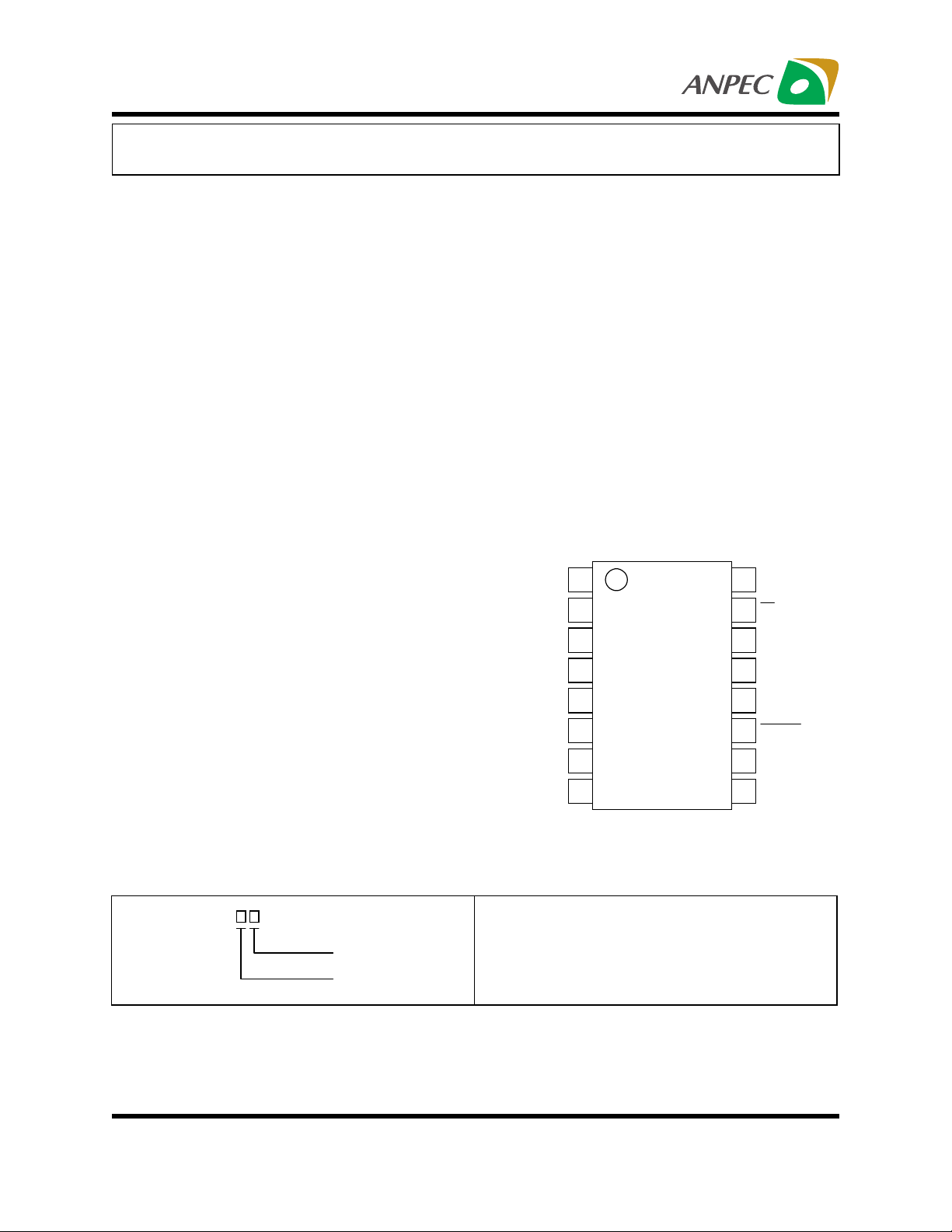
Pin Assignment
+Vcc 1
X+
Y+
2
3
DCLK
16
15
CS
14
DIN
4
X-
5
Y-
6
GND
7
IN4 V
8
13
12
11
10IN3
9
BUSY
DOUT
PENIRQ
+Vcc
REF
Order Information
APT7843
Temp. Range
Package Code
ANPEC reserves the right to make changes to improve reliability or manufacturability without notice, and advise
customers to obtain the latest version of relevant information to verify before placing orders.
Package Code
N : SSOP O : TSSOP
Temp. Range
I : - 40 to 85 C
°
Copyright ANPEC Electronics Corp.
Rev. A.8 - Apr., 2002
www.anpec.com.tw1
APT7843
y)
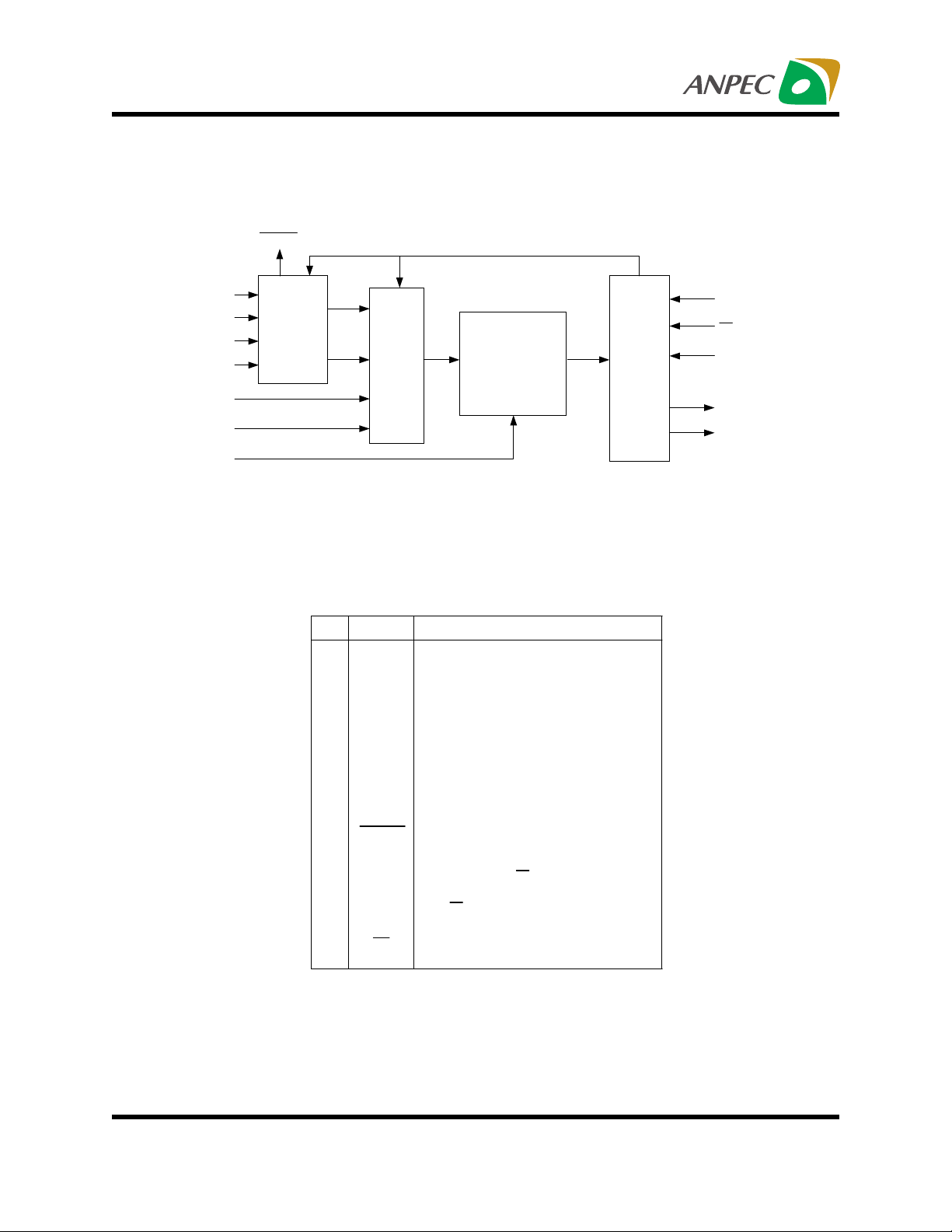
Block Diagram
PENIRQ
X+
V
X-
Y+
Y-
IN3
IN4
REF
Screen Driver
Pin Descriptions
MUX
PIN NAME
1+Vcc
2X+
3Y+
4X-
5Y-
6GND
7IN3
8IN4
9V
REF
12 Bit or 8 Bit
A/D Converter
DESCRIPTION
Power Supply,2.2V to 5V.
Connect to X+ on touch screen.
Connect to Y+ on touch screen.
Connect to X- on touch screen.
Connect to Y- on touch screen.
Ground
Auxiliary Input of A/D converter.
Auxiliary input of A/D converter.
Voltage Reference Input.
Serial
Interface
10 +Vcc Power Supply,2.2V to 5V.
11 PENIRQ Pen interrupt. Open anode output (requires
10k
to 100k
pull-up resistor externall
12 DOUT Serial Data Output. This output is high
impedance when CS is HIGH.
13 BUSY Busy Output. This output is high impedance
CS
when
is HIGH.
14 DIN Serial Data input.
15 CS Chip Select. (Active Low)
16 DCLK Serial Clock.
DCLK
CS
DIN
DOUT
BUSY
Copyright ANPEC Electronics Corp.
Rev. A.8 - Apr., 2002
www.anpec.com.tw2
APT7843
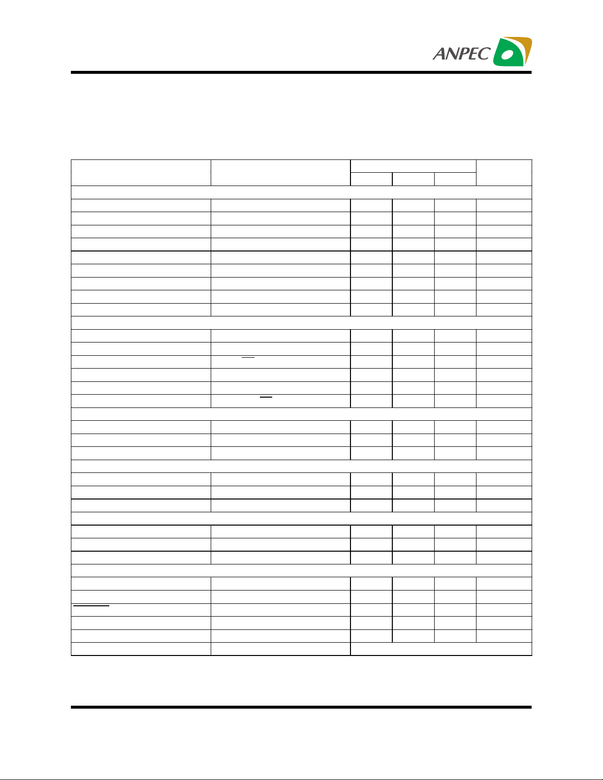
Electrical Characteristics
At TA = -40°C to 85°C , V
= +2.7V , V
CC
= +2.5V , f
REF
= 125kHz , f
SAMPLE
CLK
= 16 • f
= 2MHz , 12-bit mode
SAMPLE
, and digital inputs = GND or Vcc , unless otherwise noted.
PARAMETER CONDITIONS
MIN TYP MAX
DC ACCURACY
Resolution 12 Bits
No missing code 11 Bits
Integral Nonlinearity
Offset E rro r
Offset E rro r M atch 0.1 1 LS B
Gain Error
Gain Error Match 0.1 1 LSB
Noise 30 uV rms
Power Supply Rejection 70 dB
REFERANCE INPUT
V
Input Voltage Range 1.0 Vcc
REF
DC Leakage Current
V
Input Impedance CS = GND or Vcc 5
REF
V
Input Current 13 40
REF
F
= 12.5 kH z 2.5
SAMPLE
CS = Vcc 3
DYNAMIC PERFORENCE
Aperture Delay 30 ns
Aperture Jitter 100 ps
Channel to Channel Isolation VIN = 2.5Vp-p ; FIN = 50kHz 100 dB
CONVERSION RATE
Conversion Time 12 DCLK cycles
Track/H old A cqu isition Time 3 DCLK cycles
Throughput Rate 125 KSPS
SWITCH DRIVERS
On-Resistance
Y+ , X+ 415
Y- , X- 415
LOGIC OUTPUTS
Output High Voltage , V
Output Low Voltage , V
OH
OL
PENIRQ output low voltage , V
OL
|IOH| ≤ -250µA Vcc–0.2 V
|IOL| ≤ 250µA
Floating-State Leakage Current
Floating-State Output Capacitance 10 pF
Output Coding Straight ( Natural ) Binary
APT7843
1
±
UNITS
2LSB
±
6LSB
±
4LSB
±
A
µ
G
Ω
A
µ
A
µ
A
µ
Ω
Ω
0.4 V
0.2 V
±
10
A
µ
Note : (1) LSB means least Significant Bit. With V
Copyright ANPEC Electronics Corp.
Rev. A.8 - Apr., 2002
equal to +2.5V , one LSB is 610µV
REF
www.anpec.com.tw3

APT7843
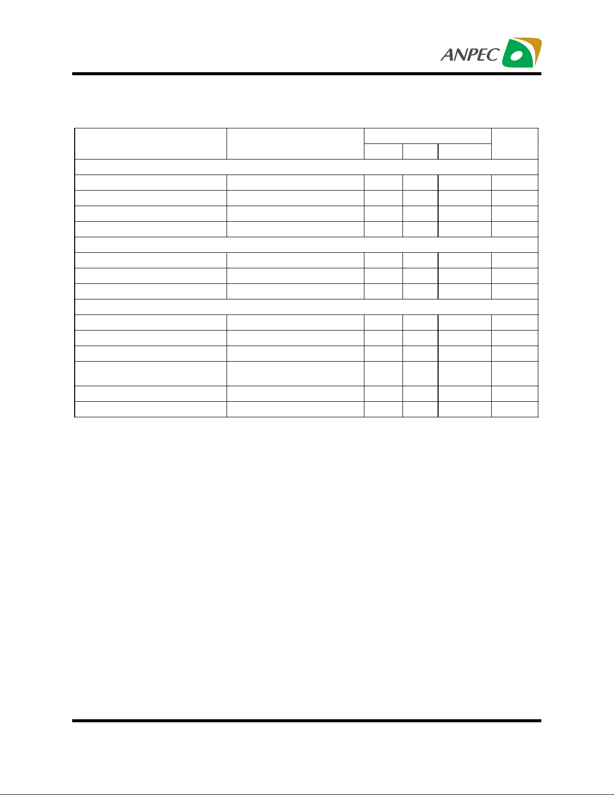
Electrical Characteristics (Cont.)
PARAMETER CONDITIONS
APT7843
MIN TYP MAX
UNITS
LOGIC INPUTS
Input High Voltage ,
V
INH
Input Low Voltage ,
V
INL
Input Current , I
IN
Input Capacitance ,
C
IN
|I
| ≤ +5µA2.4 V
INH
|I
| ≤ +5µA0.8V
INL
1
±
µ
10 pF
ANALOG INPUT
Input Voltage Ranges 0 V
DC Leakage Current
0.1
±
REF
Volts
µ
Input Capacitance 30 pF
POWER REQUIREMENTS
Vcc 2.7 3.6 V
Icc Digital I/Ps =0V or Vcc
Normal Mode (Static) Vcc = 3.6V 650
Normal Mode (F
12.5kSPS)
Shutdown
Mode(Static)
SAMPLE
=
Vcc = 3.6V 540
3
Showdown Vcc = 3.6V 3.6
µ
µ
µ
µ
A
A
A
A
A
W
Copyright ANPEC Electronics Corp.
Rev. A.8 - Apr., 2002
www.anpec.com.tw4

APT7843
Electrical Characteristics
At TA = -40°C to 85°C, V
= +2.4V , V
CC
don’t care, f
REF
= 1.25KHz, f
SAMPLE
CLK
= 16 • f
= 20KHz, 8-bit
SAMPLE
differential mode, no support single end mode, and digital inputs = GND or Vcc , unless otherwise noted.
PARAMETER CONDITIONS
MIN TYP MAX
APT7843
UNITS
DC ACCURACY
Resolution 8 Bits
No missing code 7 Bits
Integral Nonlinearity
Offset Error
2LSB
±
6LSB
±
Offset Error Match 0.1 1 LSB
Gain Error
4LSB
±
Gain Error Match 0.1 1 LSB
Noise 30 uV rms
Power Supply Rejection 70 dB
DYNAMIC PERFORENCE
Aperture Delay 30 ns
Aperture Jitter 100 ps
Channel to Channel Isolation VIN = 2.5Vp-p ; FIN = 50kHz 100 dB
CONVERSION RATE
Conversion Time 12 DCLK cycles
Track/Hold Acquisition Time 3 DCLK cycles
Throughput Rate 1.25 KSPS
SWITCH DRIVERS
On-Resistance
Y+ , X+ 4
Y- , X- 4
Ω
Ω
LOGIC OUTPUTS
Output High Voltage , V
Output Low Voltage , V
OH
OL
PENIRQ output low voltage , V
Floating-State Leakage Current
OL
|IOH| ≤ -250µA Vcc–0.2 V
|IOL| ≤ 250µA0.4V
0.2 V
±
10
A
µ
Floating-State Output Capacitance 10 pF
Output Coding Straight ( Natural ) Binary
Copyright ANPEC Electronics Corp.
Rev. A.8 - Apr., 2002
www.anpec.com.tw5
APT7843
Electrical Characteristics (Cont.)
PARAMETER CONDITIONS
APT7843
MIN TYP MAX
UNITS
LOGIC INPUTS
Input High Voltage , V
Input Low Voltage , V
Input Current , I
IN
Input Capacitance , C
INH
INL
IN
|I
| ≤ +5µA2.2 V
INH
|I
| ≤ +5µA0.6V
INL
+0.2 V
DD
1
±
µ
10 pF
ANALOG INPUT
Input Voltage Ranges 0 V
DC Leakage Current
0.1
±
REF
Volts
µ
Input Capacitance 30 pF
POWER REQUIREMENTS
Vcc 2.2 2.4 3.6 V
Icc Digital I/Ps =0V or Vcc
Normal Mode (Static) Vcc = 2.4V 280 650
Norm al Mode (F
12.5kSPS)
SAMPLE
=
Vcc = 2.4V 540
Shutdown Mode(Static) 3
Showdown Vcc = 2.4V 3.6
µ
µ
µ
µ
A
A
A
A
A
W
Copyright ANPEC Electronics Corp.
Rev. A.8 - Apr., 2002
www.anpec.com.tw6
 Loading...