

ANPEC APR3003-43BC-TR, APR3003-43AI-TR, APR3003-43AC-TR, APR3003-39DI-TR, APR3003-39DC-TR Datasheet
...
Copyright ANPEC Electronics Corp.
Rev. A.2 - Oct., 2003
APR3001/2/3
www.anpec.com.tw1
ANPEC reserves the right to make changes to improve reliability or manufacturability without notice, and advise
customers to obtain the latest version of relevant information to verify before placing orders.
MicroPower Microprocessor Reset Circuit 5555555555.9
Features General Description
Applications
•
Computers
• Cell Phones
• Portable Electronics
• µP Power Supply Monitoring
The APR3001/2/3 are designed to monitor voltage
supplies in µP and digital systems. The quiescent
current is extremely low, typically 1.5 µA, making it
ideal for portable battery operated equipment. The
APR3001/2/3 operate by monitoring the system
power supply voltage. When the input voltage drops
below a fixed threshold, the device asserts a reset
signal for a fixed time period after Vcc rises above
the fixed threshold. The APR3001/2/3 series is available with three output stage versions : APR3001
push-pull active low output, APR3002 push-pull active high output and APR3003 open drain active low
output. They are also designed to reject fast line transient glitches on Vcc. The APR3001/2/3 are come in
a miniature SOT-23, SOT-23-5, SOT-89 packages.
• 1.2V to 6V Input Voltage Range
• Low Quiescent Current : less Than 1.5 µA
• High accuracy detection threshold : ±1.5%
• Fixed trimmed reset thresholds for 1.5V, 1.75V,
2.32V, 2.63V, 2.93V, 3.08V, 3.9V, 4.38V.
• Reset Timeout Period 250ms
• Available output configurations
- Open-drain output
- CMOS active high output
- CMOS active low output
• SOT-23 , SOT-23-5 and SOT-89 packages
• No external components
Pin Configuration
SOT-23 (Top View)
Reset
12
3
GND
V
CC
Reset
(3001/3)
(3002)
SOT-23-5 (Top View)
SOT-89 (Top View)
VCCGND
NCNC
123
45
Reset
Reset
(3001/3)
(3002)
GNDV
CC
213
Reset
Reset
(3001/3)
(3002)
Copyright ANPEC Electronics Corp.
Rev. A.2 - Oct., 2003
APR3001/2/3
www.anpec.com.tw2
Package Code
A : SOT-23 B : SO T-2 3-5 D : SO T -89
Temp. Range
C : 0 to 7 0 C I : -40 to 85 C
Handling Code
TR : Tape & Reel
Voltage Code :
15 : 1.5V ~ 43 : 4.38V
APR30 01/2/3 -
Handling Code
Temp. Range
Package Code
Voltage Code
Date C od e
X X
Voltage Code
01/2/3
APR3001/2/3
XXXXX 15
XXXXX - Date Code ; 15 - 1.5VAPR3001/2/3 -15 D :
APR3001/2/3 A/B :
A:1.5V B:1.75V C:2.32V D:2.63V E:2.93V F:3.08V G:3.9V H:4.38V
Ordering and Marking Information
°°
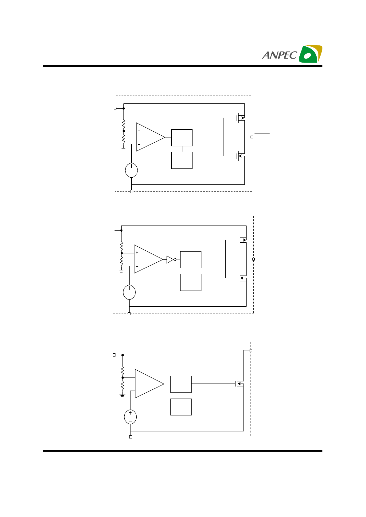
Absolute Maximum Ratings
Symbol Parameter Value Unit
VCC V
CC
to GND -0.3 to 6 V
RESET to GND (Push-Pull Output) -0.3 to VCC +0.3
V
RESET
RESET to GND (Open Drain Output) -0.3 to 6
V
I
MAX
Maximum Continuous Input Current 20 mA
I
RESET
RESET/RESET Current 20 mA
dVcc/dt Rate of Rise of VCC 100
V/µs
TJ Junction Temperature Range -40 to 150 °C
TL Lead Temperature (Soldering, 10 second) 260 °C
SOT-23 357
SOT-23-5 357
R
TH,JA
Thermal Resistance – Junction to Ambient
SOT-89 180
°C/W
PD Power Dissipation Internally Limited W
Pin Function Descrpition
PIN
No. Name
Description
RESET
(APR3001/3)
RESET output remains l ow while VCC is below the reset thr eshold and remains
so for a fixed time period after VCC raises above the reset threshold
1
RESET
(APR3002)
RESET output rem ains high while V
CC
is below the res et threshold and rem ains
so for a fixed time period after VCC raises above the reset threshold.
2 GND Ground connection
3 VCC Supply Voltage (+1.2V to +6V)
Note: The pin sequence here might not be correct for all different package types, and please refer pin
configuration in page1 for correct pin assignment.
Copyright ANPEC Electronics Corp.
Rev. A.2 - Oct., 2003
APR3001/2/3
www.anpec.com.tw3
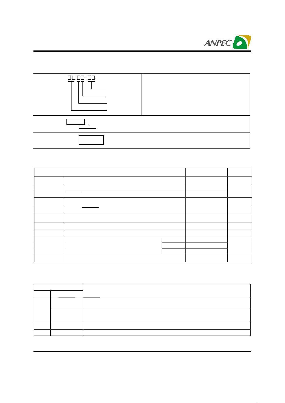
Block Diagram
V
c c
GND
V
REF
Reset
Generator
+ Timer
Oscillator
RESET
APR3001
V
c c
GND
V
REF
Reset
Generator
+ Timer
Oscillator
RESET
APR3002
V
c c
GND
V
REF
Reset
Generator
+ Timer
Oscillator
RESET
APR3003
Copyright ANPEC Electronics Corp.
Rev. A.2 - Oct., 2003
APR3001/2/3
www.anpec.com.tw4
Part Number Description
Part Number Part Description
APR3001 Reset Output Push Pull Active Low with Delay
APR3002 Reset Output Push Pull Active High with Delay
APR3003 Reset Output Open Drain Active Low with Delay
Electrical Characteristics
VIN = 5V, TA = -40 to 85°C unless otherwise noted. T ypical values are at TA=25°C, VCC = 5V for 4.38V
versions, VCC = 3.3V for 3.08/2.93V versions, VCC = 3.0V for 2.63V. versions and VCC = 2.5V for 2.32V
versions, VCC = 2.0V for 1.75V versions , VCC = 1.8V for 1.5V versions.
APR3001/2/3
Symbol
Parameter Test Conditions
Min. Typ. Max.
Unit
VCC
Supply Voltage
1.2 6
V
ICC
Supply Current V
CC
=1.5V~6V 1.5 4
µA
T
A
=-40 to 85°C 3 5
T A=25°C ±1.5%
VTH
Reset Threshold
T
A
=-40 to 85°C ±2%
V
HYST
Hysteresis Range 20 mV
T
RTP
Reset Timeout Period
150 250 350
ms
VOL
Reset Output Low I
SINK
=1.2mA 0.5 V
VOH
Reset Output High I
SOURCE
=0.6mA 0.8*VCC
TD
V
CC
to Reset Delay VCC=VTH to (VTH-100mV) 25
µS
ILE
Reset Output Leakage 0.5
µA
V
CC
V
CC
GND
100k
APR3003 RESET
RESET
INPUT
µP
V
CC
GND
V
CC
V
CC
GND
RESET
(RESET)
RESET
INPUT
µP
V
CC
GND
APR3001
APR3002
Application Circuit
Copyright ANPEC Electronics Corp.
Rev. A.2 - Oct., 2003
APR3001/2/3
www.anpec.com.tw5
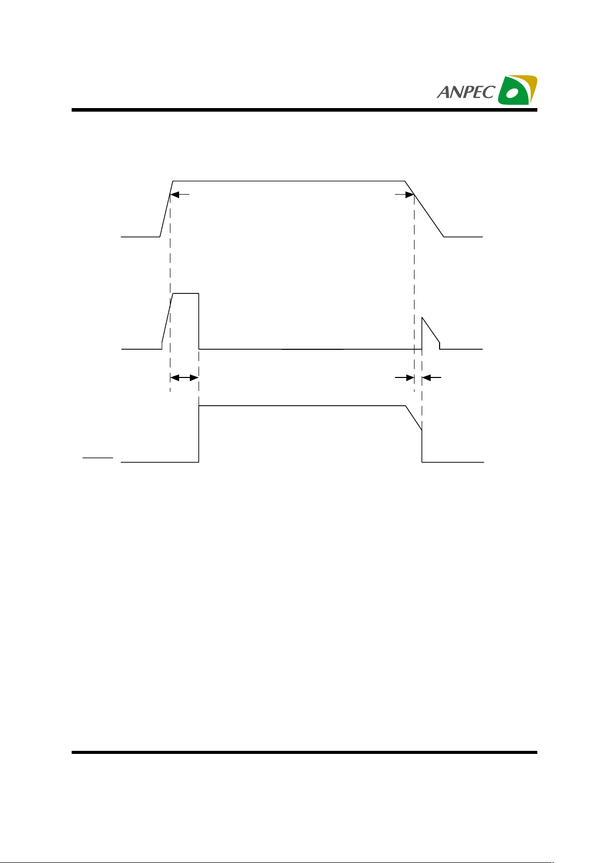
Timing Chart
Vcc
RESET
Reset Timeout Period 250ms
Vc c t o Res et Delay 25us
Reset Threshold Reset Threshold
RESET
(APR3002)
(APR3001/3)

Copyright ANPEC Electronics Corp.
Rev. A.2 - Oct., 2003
APR3001/2/3
www.anpec.com.tw6
0
5
10
15
20
25
30
35
40
45
50
0123456
Vcc=2.9V
Vcc=2V
Vcc=2.5V
Vcc=1.5
0
10
20
30
40
50
60
70
0123456
Vcc=4 V
Vcc=3 V
Vcc=5 V
0
0.4
0.8
1.2
1.6
2
0123456
0
20
40
60
80
100
120
10 100 1000
Typical Characteristics
Supply Current vs. Supply Voltage
Supply Current (uA)
Supply Voltage (V)
Maximum Transient Duration vs.
Reset Threshold Overdrive VTH - VCC
Maximum Transient Duration (us)
Reset Threshold Overdrive VTH - VCC (mV)
Output Source Current vs. Reset High Output Voltage
Output Source Current (mA)
Reset High Output Voltage (V)
Output Sink Current vs. Reset Low Output Voltage
Output Sink Current (mA)
Reset Low Output Voltage (V)
generate a reset signal
never generate a reset signal

Copyright ANPEC Electronics Corp.
Rev. A.2 - Oct., 2003
APR3001/2/3
www.anpec.com.tw7
0.994
0.996
0.998
1
1.002
1.004
1.006
1.008
-40 -20 0 20 40 60 80 100 120
0
0.5
1
1.5
2
2.5
3
3.5
-40-200 20406080100120
Vcc=3V
Vcc=5V
0
100
200
300
400
500
600
-40-200 20406080100120
0
10
20
30
40
50
60
-40-200 20406080100120
VOD=100mV
Typical Characteristics
Normalized Reset Threshold vs. T emperature
Normalized Reset Threshold (%)
T emperature (°C)
Reset Propagation Delay vs. T emperature
Reset Propagation Delay (us)
T emperature (°C)
Reset Timeout Period vs. Temperature
Reset Timeout Period (ms)
T emperature (°C)
Supply Current vs. T emperature
Supply Current (uA)
T emperature (°C)

Copyright ANPEC Electronics Corp.
Rev. A.2 - Oct., 2003
APR3001/2/3
www.anpec.com.tw8
Power Up
Typical Characteristics
Power Down
Time (200ms/div)
Vcc to RESET Delay
Vcc(0.5V/div)
Vcc=VTH to (VTH-100mV)
RESET(2V/div)
Time (10us/div)
Vcc(2V/div)
RESET(2V/div)
Vcc(2V/div)
RESET(2V/div)
Time (50ms/div)

Copyright ANPEC Electronics Corp.
Rev. A.2 - Oct., 2003
APR3001/2/3
www.anpec.com.tw9
Application Information
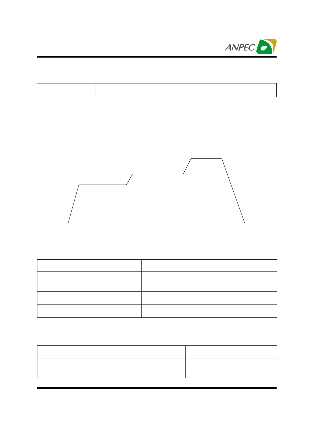
VCC Transient Rejection
The APR3001/2/3 have the function to reject the transient glitches from the power line. The Maximum Transient Duration vs. Reset Threshold Overdrive shows
at Typical Characteristics.The transient voltage with
the duration under the curve will not generate a reset
signal, e.g. a transient of 100mV below the reset
threshold voltage have the duration more than 35us, it
will generate a reset signal. Connect a 0.1uF bypass
capacitor to the VCC pin can improve the transient
immunity.
Reset Output
The APR3001/2/3 have 3 output stage versions:
APR3001 is an active low push-pull output, when the
VCC drops below the reset threshold, the RESET output generates a low signal. APR3002 is an active high
push-pull output, when the VCC drops below the reset
threshold, the RESET output generates a high signal
(see Timing Chart). APR3003 is an active low open
drain output, the RESET output must be connected a
pull-up resistor to a supply voltage that is lower than
6V, it suits to use in multiple voltage systems (see
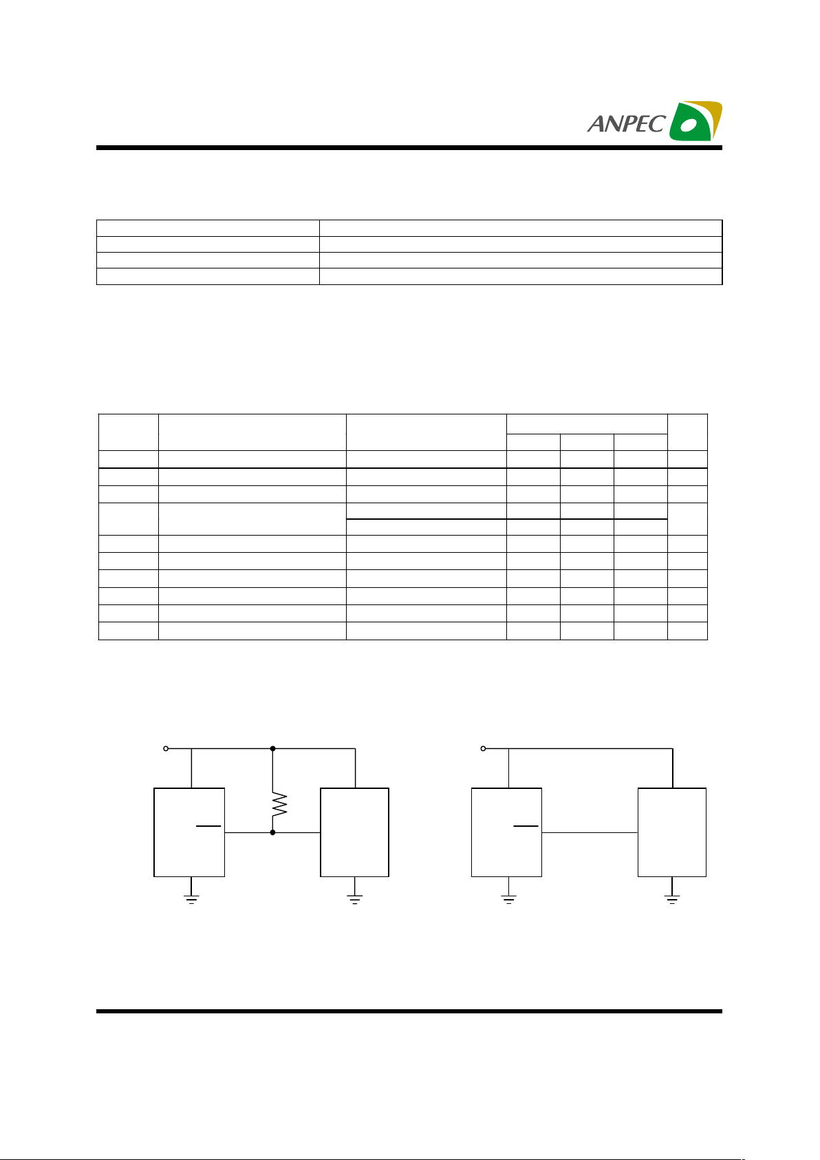
Figure 2). The APR3001 RESET output is valid until
the VCC=1.2V, below 1.2V the IC is shutdown, and
the output becomes a floating state. If it is a trouble, a
resistor should be connected from reset output to
ground to keep the reset output low (see Figure 1).
For The APR3002, a pull-up resistor to VCC is required
to keep the valid reset output for VCC below 1.2V.
RESET
V
CC
GND
V
CC
100K
Figure 1. Ensuring RESET Valid to VCC = 0 V
V
CC
APR3003
RESET
GND
+3.3V +5.0V
V
CC
GND
RESET
INPU T5VSystem
100k
Figure 2. APR3003 Open Drain Output with Multiple
Supplies

Copyright ANPEC Electronics Corp.
Rev. A.2 - Oct., 2003
APR3001/2/3
www.anpec.com.tw10
Packaging Information
SOT-23
D
E H
S
e
A
A1
L
C
B
3
2
1
Millimeters Inches
Dim
Min. Max. Min. Max.
A 1.00 1.30 0.039 0.051
A1 0.0 0 0.10 0.000 0.004
B 0.35 0.51 0.014 0.020
C 0.10 0.25 0.004 0.010
D 2.70 3.10 0.106 0.122
E 1.40 1.80 0.055 0.071
e 1.90 BSC 0.075 BSC
H 2.40 3.00 0.094 0.118
L 0.37 0.0015

Copyright ANPEC Electronics Corp.
Rev. A.2 - Oct., 2003
APR3001/2/3
www.anpec.com.tw11
Packaging Information
SOT-23-5
e1
E1 E
b
12
3
45
e
D
A2
A
A1 L 2
L
L 1
a
Millimeters Inches
Dim
Min. Max. Min. Max.
A 0.95 1.45
0.037 0.057
A1 0.05 0.15
0.002 0.006
A2 0.90 1.30
0.035 0.051
D2.83.00
0.110 0.118
E2.63.00
0.102 0.118
E1 1.5 1.70
0.059 0.067
L 0.35 0.55
0.014 0.022
L1 0.20 BSC 0.008 BSC
L2 0.5 0.7
0.020 0.028
N5 5
α
0
°
10
°
0
°
10
°

Copyright ANPEC Electronics Corp.
Rev. A.2 - Oct., 2003
APR3001/2/3
www.anpec.com.tw12
Packaging Information
SOT-89 (Reference EIAJ ED-7500A Reg stration SC-62)
D
D1
e
B1
e1
B
123
L
H
E
C
a
a
A
Millimeters Inches
Dim
Min. Max. Min. Max.
A 1.40 1.60 0.055 0.063
B 0.40 0.56 0.016 0.022
B1 0.35 0 .48 0.014 0.019
C 0.35 0 .44 0.014 0.017
D 4.40 4 .60 0.173 0.181
D1 1 .35 1.83 0.053 0.072
e 1.50 BSC 0.059 BSC
e1 3.00 BSC 0.118 BSC
E 2.29 2.60 0.090 0.102
H 3.75 4 .25 0.148 0.167
L 0.80 1 .20 0.031 0.047
α
10
°
10
°
Copyright ANPEC Electronics Corp.
Rev. A.2 - Oct., 2003
APR3001/2/3
www.anpec.com.tw13
Reflow Condition (IR/Convection or VPR Reflow)
Physical Specifications
Pre-heat temperature
183 C
Peak temperature
Time
°
temperature
Classification Reflow Profiles
Convection or IR/
Convection
VPR
Average ramp-up rate(183°C to Peak) 3°C/second max. 10 °C /second max.
Preheat temperature 125 ± 25°C)
120 seconds max
Tem perat ure m ainta ined above 183°C
60 – 150 seconds
Time within 5°C of actual peak temperature
10 –20 seconds 60 seconds
Peak temperature range
220 +5/-0°C or 235 +5/-0°C 215-219°C or 235 +5/-0°C
Ramp-down rate
6 °C /second max. 10 °C /second max.
Time 25°C to peak temperature
6 minutes max.
Package Re flow Conditions
pkg. thickness ≥≥≥≥ 2.5mm
and all bgas
pkg. thickness < 2.5mm and
pkg. volume ≥≥≥≥ 350 mm³
pkg. thickness < 2.5mm and pkg.
volume < 350mm³
Convection 220 +5/-0 °C Convection 235 +5/-0 °C
VPR 215-219 °C VPR 235 +5/-0 °C
IR/Convection 220 +5/-0 °C IR/Convection 235 +5/-0 °C
Terminal Material Solder-Plated Copper (Solder Ma te rial : 90/10 or 63/37 Sn Pb)
Lead Solderability Meets EIA Specification RSI86-91, ANSI/J-STD-002 Category 3.
Copyright ANPEC Electronics Corp.
Rev. A.2 - Oct., 2003
APR3001/2/3
www.anpec.com.tw14
Carrier Tape & Reel Dimensions
A
J
B
T2
T1
C
t
Ao
E
W
Po
P
Ko
Bo
D1
D
F
P1
Test item Method Description
SOLDERABILITY MIL-STD-883D-2003 245°C,5 SEC
HOLT MIL-STD 883D-1005.7 1000 Hrs Bias @ 125°C
PCT JESD-22-B, A102 168 Hrs, 100% RH, 121°C
TST MIL-STD 883D-1011.9 -65°C ~ 150°C, 200 Cycles
Reliability test program
Application
A B C J T1 T2 W P E
178±160 ± 1.0 12 .0 2.5 ± 0.15 9.0 ± 0.5 1.4
8.0+ 0.3
- 0.3
4.0 1.75
F D D1 Po P1 Ao Bo Ko t
SOT-23
3.5 ± 0.05 1.5 +0.1
F
0.1MIN 4.0 2.0 ± 0.05 3.1 3.0 1.3 0.2±0.03
Application
A B C J T1 T2 W P E
178 ±172 ± 1.0 13.0 + 0.2 2.5 ± 0.15 8.4 ± 2 1 .5 ± 0.3 8.0 ± 0.3 4 ± 0.1 1 .7 5± 0.1
F D D1 Po P1 Ao Bo Ko t
SOT-23-5
3.5 ± 0.05 1.5± 0.1 1.5± 0.1 4 .0 ± 0.1 2.0 ± 0.1 3.15 ± 0.1 3.2± 0.1 1.4± 0.1 0 .2±0.033
Application
A B C J T1 T2 W P E
178 ±170 ± 213.5 ± 0.15 3 ± 0.15 14 ± 2 1.3 ± 0.3
12 + 0.3
12 - 0.1
8 ± 0.1 1 .7 5± 0.1
F D D1 Po P1 Ao Bo Ko t
SOT-89
5.5 ± 0.05 1.5± 0.1 1.5± 0.1 4 .0 ± 0.1 2.0 ± 0.1 4.8 ± 0.1 4 .5± 0.1 1.8 0± 0.1 0.3±0.013

Copyright ANPEC Electronics Corp.
Rev. A.2 - Oct., 2003
APR3001/2/3
www.anpec.com.tw15
Cover Tape Dimensions
Anpec Electronics Corp.
Head Office :
5F, No. 2 Li-Hsin Road, SBIP,
Hsin-Chu, Taiwan, R.O.C.
Tel : 886-3-5642000
Fax : 886-3-5642050
Taipei Branch :
7F, No. 137, Lane 235, Pac Chiao Rd.,
Hsin Tien City, Taipei Hsien, Taiwan, R. O. C.
Tel : 886-2-89191368
Fax : 886-2-89191369
Customer Service
Application Carrier Width Co ver Tape Width Devices Per Reel
SOT- 23
8 5.3 3000
SOT- 23-5
8 5.3 3000
SOT- 89
12 9.3 1000
 Loading...