

Page 1
APM4542
Dual Enhancement Mode MOSFET (N-and P-Channel)
Features
• N-Channel
30V/7A, R
R
=17mΩ(typ.) @ VGS=10V
DS(ON)
=22mΩ(typ.) @ VGS=4.5V
DS(ON)
• P-Channel
-30V/-5.5A,R
R
••
• Super High Dense Cell Design for Extremely
••
Low R
••
• Reliable and Rugged
••
••
• SO-8 Package
••
DS(ON)
=35mΩ(typ.) @ VGS=-10V
DS(ON)
=51mΩ(typ.) @ VGS=-4.5V
DS(ON)
Applications
• Power Management in Notebook Computer ,
Portable Equipment and Battery Powered
Systems.
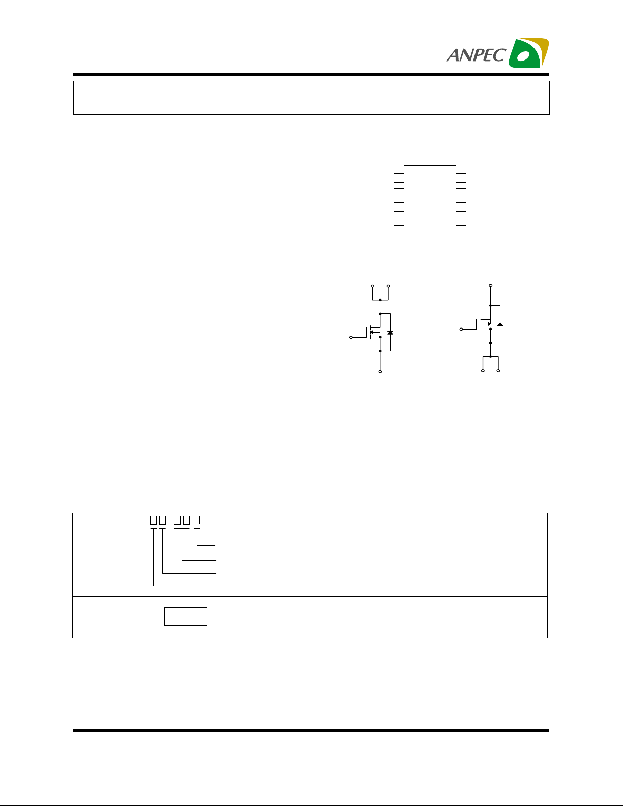
Pin Description
1
2
G1
3
S2
45
G2 D2
SO-8
D1 D1
G1
S1
N-Channel MOSFET
8S1
D1
7
D1
6
D2
S2
G2
D2 D2
P-Channel MOSFET
Ordering and Marking Information
APM4542
Lead Free Code
Handling Code
Temp. Range
Package Code
APM4542 K :
ANPEC reserves the right to make changes to improve reliability or manufacturability without notice, and advise
customers to obtain the latest version of relevant information to verify before placing orders.
Copyright ANPEC Electronics Corp.
Rev. A.2 - Sep., 2003
APM4542
XXXXX
Package Code
K : SO-8
Operation Junction Temp. Range
C : -55 to 1 50 C
Handling Code
TR : Tape & Reel
Lead Free Code
L : Lead Free Device Blank : Orginal Device
XXXXX - Date Co d e
°
www.anpec.com.tw1
Page 2
APM4542
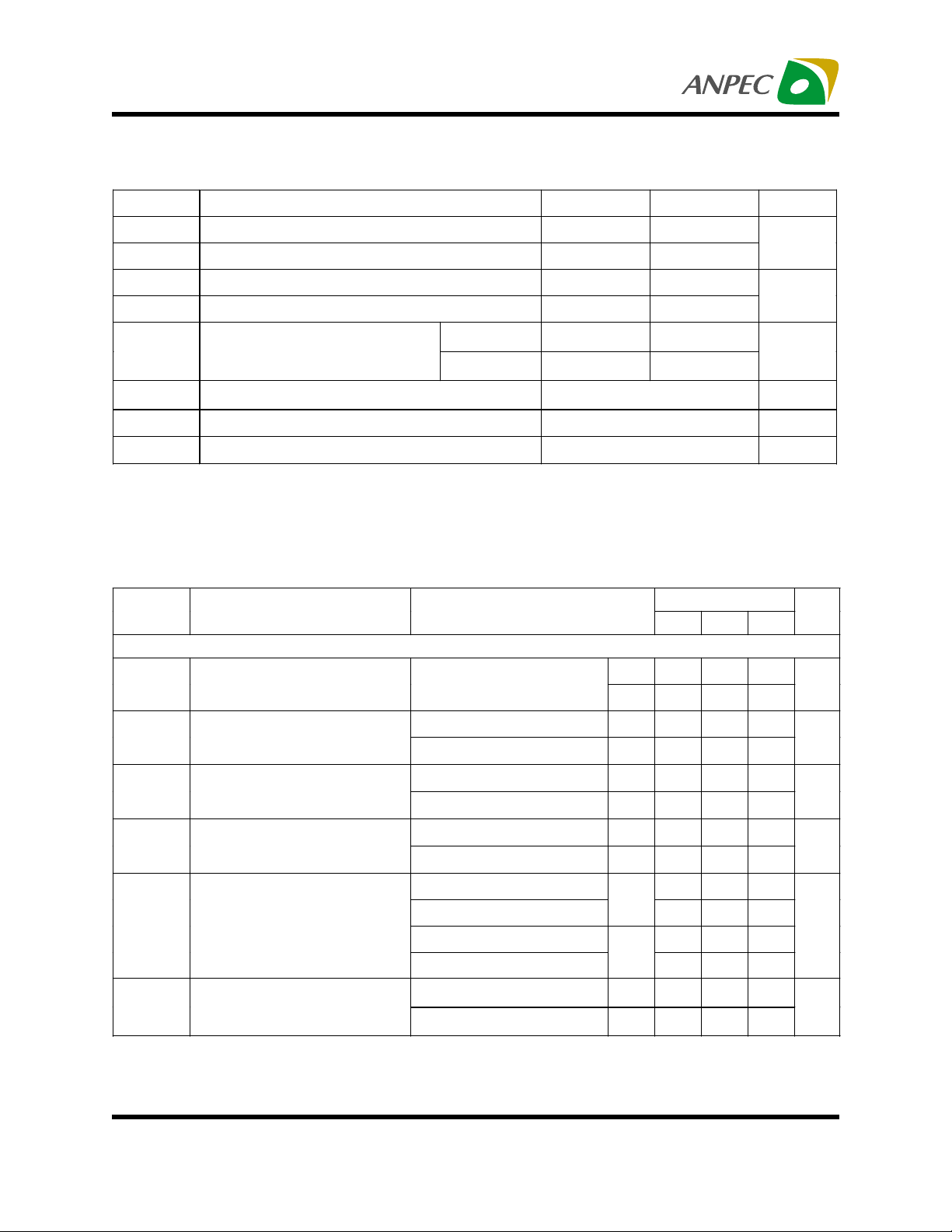
Absolute Maximum Ratings (T
= 25°C unless otherwise noted)
A
Symbol Parameter N-Channel P-Channel Unit
V
Drain-Source Voltage 30 -30
DSS
V
Gate-Source Voltage ±20 ±20
GSS
*
I
Maximum Drain Current – Continuous 7 -5
D
IDM Maximum Drain Current – Pulsed 28 -20
PD
Maximum Power Dissipation
TA=25°C
T
=100°C
A
2 2
0.8 0.8
TJ Maximum Junction Temperature 150
T
Storage Temperature Range -55 to 150
STG
R
θ
Thermal Resistance – Junction to Ambient 62.5
jA
V
A
W
°C
°C
°C/W
* Surface Mounted on FR4 Board, t ≤ 10 sec.
Electrical Characteristics (T
Symbol Parameter Test Condition
= 25°C unless otherwise noted)
A
APM4542
Min.
Typ. Max.
Unit
Static
Notes
BV
I
DSS
Drain-Source Breakdown
DSS
Voltage
Zero Gate Voltage Drain
Current
V
GS
VDS=24V , VGS=0V
V
DS
VDS=VGS , IDS=250µA
V
Gate Threshold Voltage
GS(th)
V
DS=VGS
VGS=±20V , VDS=0V
I
Gate Leakage Current
GSS
V
GS
VGS=10V , IDS=7A
Drain-Source On-state
R
a
DS(ON)
Resistance
a
V
Diode Forward Voltage
SD
a
: Pulse test ; pulse width ≤300µs, duty cycle ≤ 2%
VGS=4.5V , IDS=5A
VGS=-10V , IDS=-5.5A
V
GS
ISD=2A , VGS=0V N-Ch
I
SD
N-Ch
=0V , IDS=250µA
P-Ch
N-Ch
=-24V , VGS=0V
P-Ch
N-Ch
, IDS=-250µA
P-Ch
N-Ch
=±20V , VDS=0V
P-Ch
N-Ch
P-Ch
=-4.5V , IDS=-4A
=-2.3A , VGS=0V P-Ch
30
-30
1
-1
1 1.5 2
-1 -1.5 -2
±100
±100
17 24
22 30
35 56
51 78
0.7 1.3
-0.7 -1.3
V
µA
V
nA
mΩ
V
Copyright ANPEC Electronics Corp.
Rev. A.2 - Sep., 2003
www.anpec.com.tw2
Page 3
APM4542
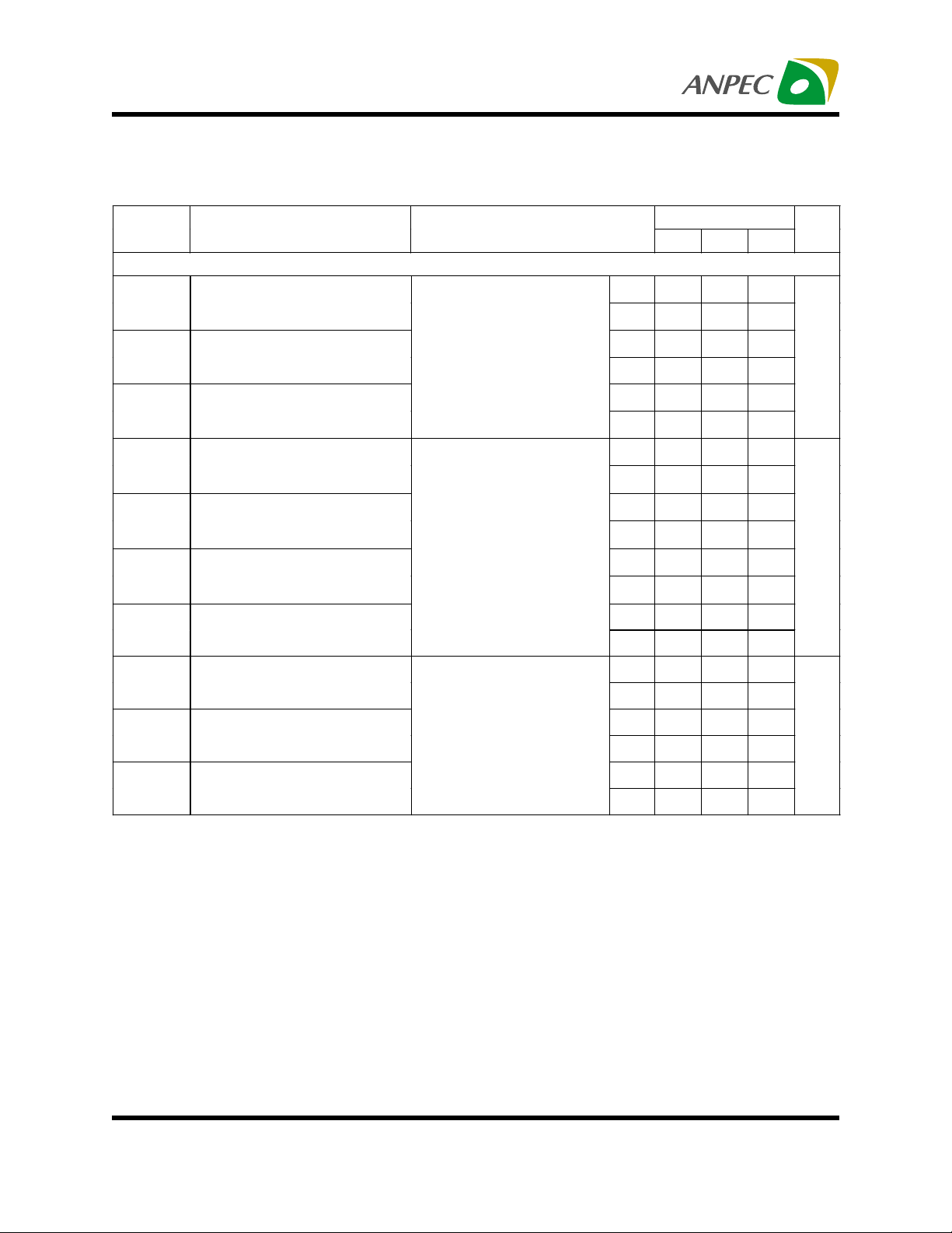
Electrical Characteristics (Cont.) (T
= 25°C unless otherwise noted)
A
Symbol Parameter Test Condition
Dynamic
t
b
Qg Total Gate Charge
Qgs Gate-Source Charge
Qgd Gate-Drain Charge
t
Turn-on Delay Time
d(ON)
Tr Turn-on Rise Time
Turn-off Delay Time
d(OFF)
Tf Turn-off Fall Time
C
Input Capacitance
iss
C
Output Capacitance
oss
C
Reverse Transfer Capacitance
rss
N-Channel
=15V , IDS= 7A
V
DS
V
=10V
GS
P-Channel
=-15V , IDS=-5.5A
V
DS
=-10V
V
GS
N-Channel
=15V , IDS=2A ,
V
DD
=10V , RG=6Ω ,
V
GEN
R
=7.5Ω
L
P-Channel
=-15V , IDS=-2A ,
V
DD
=-10V , RG=6Ω,
V
GEN
R
=7.5Ω
L
N-Channel
=0V, VDS=25V
V
GS
Frequency=1.0MHz
P-Channel
=0V, VDS=-25V
V
GS
Frequency=1.0MHz
N-Ch
P-Ch
N-Ch
P-Ch
N-Ch
P-Ch
N-Ch
P-Ch
N-Ch
P-Ch
N-Ch
P-Ch
N-Ch
P-Ch
N-Ch
P-Ch
N-Ch
P-Ch
N-Ch
P-Ch
APM4542
Min.
Typ. Max.
19 28
28 36
1.6
5
3.6
4
11 20
12 24
17 28
15 29
36 62
35 60
20 36
15 30
835
950
145
160
15
110
Unit
nC
ns
pF
Notes
b
: Guaranteed by design, not subject to production testing
Copyright ANPEC Electronics Corp.
Rev. A.2 - Sep., 2003
www.anpec.com.tw3
Page 4
APM4542
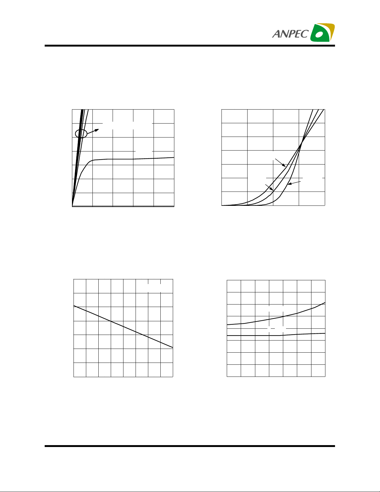
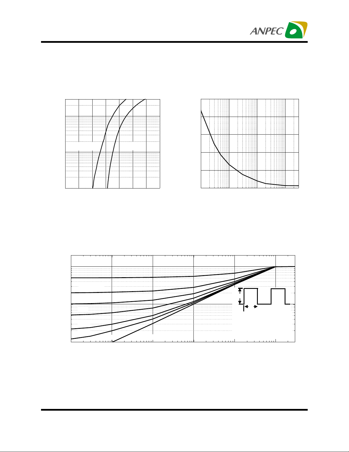
Typical Characteristics
N-Channel
Output Characteristics
28
24
20
16
12
8
-Drain Current (A)
D
I
4
0
012345
VDS-Drain-to-Source Voltage (V)
Threshold Voltage vs. Junction Temperature
1.6
1.4
VGS= 4,5,6,7,8,9,10V
VGS=3V
VGS=2V
IDS =250µA
Transfer Characteristics
28
24
20
16
12
8
-Drain Current (A)
D
I
4
0
1.5 2.0 2.5 3.0 3.5
Tj=25oC
Tj=125oC
Tj=-55oC
VGS-Gate-to-Source Voltage (V)
On-Resistance vs. Drain Current
0.040
0.035
1.2
1.0
0.8
(Normalized)
0.6
-Threshold Voltage (V)
GS(th)
0.4
V
0.2
-50 -25 0 25 50 75 100 125 150
Tj-Junction Temperature (°C)
Copyright ANPEC Electronics Corp.
Rev. A.2 - Sep., 2003
0.030
0.025
0.020
0.015
0.010
RDS(on)-On-Resistance (Ω)
0.005
0.000
0 4 8 1216202428
VGS=4.5V
VGS=10V
IDS-Drain Current (A)
www.anpec.com.tw4
Page 5

APM4542
Typical Characteristics (Cont.)
N-Channel
On-Resistance vs. Gate-to-Source Voltage
0.8
0.7
0.6
0.5
0.4
0.3
0.2
DS(on)-On-Resistance (Ω)
R
0.1
0.0
0246810
VGS-Gate-to-Source Voltage (V) Tj-Junction Temperature (°C)
10
VDS=15V
I
=7A
DS
8
6
4
2
-Gate-to-Source Voltage (V)
GS
V
0
048121620
Gate Charge
ID= 7A
On-Resistaence vs. Junction Temperature
1.8
VGS = 10V
1.6
I
= 7A
DS
1.4
1.2
1.0
(Normalized)
0.8
0.6
RDS(on)-On-Resistance (Ω)
0.4
-50 -25 0 25 50 75 100 125 150
Capacitance Characteristics
1200
1000
800
600
400
Frequency=1MHz
Ciss
C-Capacitance (pF)
200
0
0 5 10 15 20 25 30
Coss
Crss
QG-Total Gate Charge (nC)
Copyright ANPEC Electronics Corp.
Rev. A.2 - Sep., 2003
VDS-Drain-to-Source Voltage (V)
www.anpec.com.tw5
Page 6
APM4542
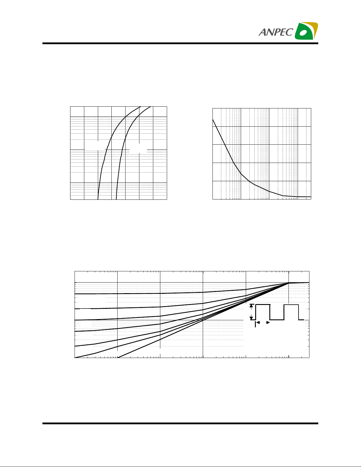
Typical Characteristics (Cont.)
N-Channel
Source-Drain Diode Forward Voltage
30
10
1
-Source Current (A)
S
I
0.1
Tj=150oC
0.0 0.2 0.4 0.6 0.8 1.0 1.2 1.4
Tj=25oC
VSD-Source-to-Drain Voltage
Normalized Transient Thermal Transient Impedence, Junction to Ambient
2
Single Pulse Power
75
60
45
30
Power (W)
15
0
0.01 0.1 1 10 30
Time (sec)
1
Duty Cycle=0.5
D=0.2
0.1
D=0.1
Thermal Impedance
Normalized Effective Transient
0.01
D=0.05
D=0.02
D=0.01
1E-4 1E-3 0.01 0.1 1 10 30
Copyright ANPEC Electronics Corp.
Rev. A.2 - Sep., 2003
SINGLE PULSE
Square Wave Pulse Duration (sec)
P
DM
t
1
t
1.Duty Cycle, D= t1/t2
2.Pe r U nit Base = R
3.TJM-TA=PDMZ
4.Surface Mounted
2
thJA
thJA
www.anpec.com.tw6
=62.5oC/W
Page 7

APM4542
Typical Characteristics
P-Channel
Output Characteristics
20
15
10
-ID-Drain Current (A)
5
0
0246810
-VGS= 4,5,6,7,8,9,10V
-VGS=3V
-VDS - Drain-to-Source Voltage (V)
Transfer Characteristics
20
15
10
5
-ID-Drain Current (A)
0
012345
Tj=125oC
Tj=25oC
Tj=-55oC
-VGS - Gate-to-Source Voltage (V)
Threshold Voltage vs. Junction Temperature
1.75
1.50
1.25
1.00
0.75
(Normalized)
0.50
0.25
-VGS(th)-Threshold Voltage (V)
0.00
-50 -25 0 25 50 75 100 125 150
Tj - Junction Temperature (°C)
Copyright ANPEC Electronics Corp.
Rev. A.2 - Sep., 2003
-IDS=250
µΑ
On-Resistance vs. Drain Current
0.105
0.090
0.075
VGS=-4.5V
0.060
0.045
0.030
RDS(on)-On-Resistance (Ω)
0.015
0.000
0 5 10 15 20
VGS=-10V
-ID - Drain Current (A)
www.anpec.com.tw7
Page 8

APM4542
Typical Characteristics (Cont.)
P-Channel
On-Resistance vs. Gate-to-Source Voltage
0.150
0.125
0.100
0.075
0.050
0.025
RDS(on)-On-Resistance (Ω)
0.000
2345678910
-VGS - Gate-to-Source Voltage (V)
-ID= 5.5A
Gate Charge
10
-VDS=15 V
-I
8
= 5.5 A
DS
On-Resistance vs. Junction Temperature
1.8
-VGS = 10V
1.6
-I
= 5.5A
DS
1.4
1.2
1.0
(Normalized)
0.8
RDS(on)-On-Resistance (Ω)
0.6
0.4
-50 -25 0 25 50 75 100 125 150
TJ - Junction Temperature (°C)
1500
1250
Capacitance
Frequency=1MHz
6
4
2
-VGS-Gate-Source Voltage (V)
0
0 5 10 15 20 25 30
QG - Gate Charge (nC)
Copyright ANPEC Electronics Corp.
Rev. A.2 - Sep., 2003
1000
750
500
Ciss
Capacitance (pF)
250
0
0 5 10 15 20 25 30
Coss
-VDS - Drain-to-Source Voltage (V)
www.anpec.com.tw8
Crss
Page 9
APM4542
Typical Characteristics (Cont.)
P-Channel
Source-Drain Diode Forward Voltage
20
10
1
-Source Current (A)
S
-I
0.1
0.0 0.2 0.4 0.6 0.8 1.0 1.2 1.4
Tj=150oC
Tj=25oC
-VSD-Source-to-Drain Voltage (V )
Normalized Thermal Transient Impedance, Junction to Ambient
2
Single Pulse Power
75
60
45
30
Power (W)
15
0
0.01 0.1 1 10 30
Time (sec)
1
Duty Cycle=0.5
D=0.2
0.1
D=0.1
Thermal Impedance
Normalized Effective Transient
Copyright ANPEC Electronics Corp.
Rev. A.2 - Sep., 2003
D=0.05
D=0.02
0.01
1E-4 1E-3 0.01 0.1 1 10 30
D=0.01
SINGLE PULSE
Square Wave Pulse Duration (sec)
P
DM
t
1
t
1.Du ty C y cle , D = t1/t 2
2.Per Unit Base=R
3.TJM-TA=PDMZ
4.Surface Mounted
2
thJA
thJA
www.anpec.com.tw9
=62.5oC/W
Page 10

APM4542
Packaging Information
SOP-8 pin ( Reference JEDEC Registration MS-012)
HE
0.015X45
e1 e2
D
A1
A
1
L
0.004max.
Dim
A 1.35 1.75 0.053 0.069
A1 0.10 0.25 0.004 0.010
D 4.80 5.00 0.189 0.197
E 3.80 4.00 0.150 0.157
H 5.80 6.20 0.228 0.244
L 0.40 1.27 0.016 0.050
e1 0.33 0.51 0.013 0.020
e2 1.27BSC 0.50BSC
18
φ
Millimeters Inches
Min. Max. Min. Max.
°
8
°
Copyright ANPEC Electronics Corp.
Rev. A.2 - Sep., 2003
www.anpec.com.tw10
Page 11

APM4542
Physical Specifications
Terminal Material Solder-Plated Copper (Solder Material : 90/10 or 63/37 SnPb)
Lead Solderability Meets EIA Specification RSI86-91, A NSI/J-STD-002 C a teg ory 3 .
Reflow Condition (IR/Convection or VPR Reflow)
Reference JEDEC Standard J-STD-020A APRIL 1999
Peak temperature
temperature
Pre-heat temperature
°
183 C
Time
Classification Reflow Profiles
Convection or IR/
Convection
Average ramp-up rate(183°C to Peak) 3°C/second max. 10 °C /second max .
Preheat temperature 125 ± 25°C)
Temperature maintained above 183°C
Time within 5°C of actual peak temperature
Peak temperature range
Ramp-down rate
Time 25°C to peak temperature
120 seconds max
60 – 150 seconds
10 –20 seconds 60 seconds
220 +5/-0°C or 235 +5/-0°C 215-219°C or 235 +5/-0°C
6 °C /second max . 10 °C /second max .
6 minutes max.
VPR
Package Reflow Conditions
pkg. thickness
and all bgas
Convection 220 +5/-0 °C Convection 235 +5/- 0 °C
VPR 215-219 °C VPR 235 +5/-0 °C
IR/Convection 220 +5/-0 °C IR/Convection 235 +5/-0 °C
Copyright ANPEC Electronics Corp.
Rev. A.2 - Sep., 2003
2.5mm
≥≥≥≥
pkg. thickness < 2.5mm and
pkg. volume
350 mm³
≥≥≥≥
pkg. thickness < 2.5mm and pkg.
volume < 350mm³
www.anpec.com.tw11
Page 12

APM4542
Reliability test program
T est item Method Description
SOLDERABILITY MIL-STD-883D-2003 245°C,5 SEC
HOLT MIL-STD 883D-1005.7 1000 Hrs Bias @ 125°C
PCT JESD-22-B, A102 168 Hrs, 100% RH, 121°C
TST MIL-STD 883D-1011.9 -65°C ~ 150°C, 200 Cycles
Carrier Tape & Reel Dimensions
t
W
E
F
Po
A
P
P1
Ao
J
D
Bo
D1
C
Ko
T2
B
T1
Application A B C J T1 T2 W P E
330 ± 162 +1.5
F D D1 Po P1 Ao Bo Ko tSOP- 8
5.5± 1 1.55 +0.1 1.55+ 0.25 4.0 ± 0.1 2.0 ± 0.1 6.4 ± 0.1 5.2± 0. 1 2.1± 0.1 0.3±0.013
Copyright ANPEC Electronics Corp.
Rev. A.2 - Sep., 2003
12.75+
0.15
2 ± 0.5 12.4 ± 0.2 2 ± 0.2 1 2± 0. 3 8± 0.1 1 .75±0.1
www.anpec.com.tw12
Page 13

APM4542
Cover Tape Dimensions
Application Carrier Width Cover Tape Width Devices Per Reel
SOP- 8
Customer Service
Anpec Electronics Corp.
Head Office :
5F, No. 2 Li-Hsin Road, SBIP,
Hsin-Chu, T aiwan, R.O.C.
T el : 886-3-5642000
Fax : 886-3-5642050
Taipei Branch :
7F, No. 137, Lane 235, Pac Chiao Rd.,
Hsin Tien City, Taipei Hsien, Taiwan, R. O. C.
T el : 886-2-89191368
Fax : 886-2-89191369
12 9.3 2500
Copyright ANPEC Electronics Corp.
Rev. A.2 - Sep., 2003
www.anpec.com.tw13
 Loading...