

APL5930
3A, Ultra Low Dropout (0.23V Typical) Linear Regulator
Features
• Compatible with APL5913
• Ultra Low Dropout
- 0.23V(typical) at 3A Output Current
• Low ESR Output Capacitor (Multi-layer
Chip Capacitors (MLCC)) Applicable
• 0.8V Reference Voltage
• High Output Accuracy
- ±1.5% over Line, Load, and Temperature Range
• Fast Transient Response
• Adjustable Output Voltage
• Power-On-Reset Monitoring on Both VCNTL and
VIN Pins
• Internal Soft-Start
• Current-Limit and Short Current-Limit Protections
• Thermal Shutdown with Hysteresis
• Open-Drain VOUT Voltage Indicator (POK)
• Low Shutdown Quiescent Current (<30 µA)
• Shutdown/Enable Control Function
• Simple SOP-8P Package with Exposed Pad
• Lead Free and Green Devices Available
(RoHS Compliant)
General Description
The APL5930 is a 3A ultra low dropout linear regulator.
The IC needs two supply voltages, one is a control voltage
(V
) for the control circuitry, the other is a main supply
CNTL
voltage (VIN) for power conversion, to reduce power dissipation and provide extremely low dropout voltage.
The APL5930 integrates many functions. A Power-OnReset (POR) circuit monitors both supply voltages on
VCNTL and VIN pins to prevent erroneous operations.
The functions of thermal shutdown and current-limit protect the device against thermal and current over-loads. A
POK indicates the output voltage status with a delay time
set internally. It can control other converter for power
sequence. The APL5930 can be enabled by other power
systems. Pulling and holding the EN voltage below 0.4V
shuts off the output.
The APL5930 is available in a SOP-8P package which
features small size as SOP-8 and an Exposed Pad to
reduce the junction-to-case resistance to extend power
range of applications.
Applications
• Front Side Bus VTT (1.2V/3A)
• Note Book PC Applications
• Motherboard Applications
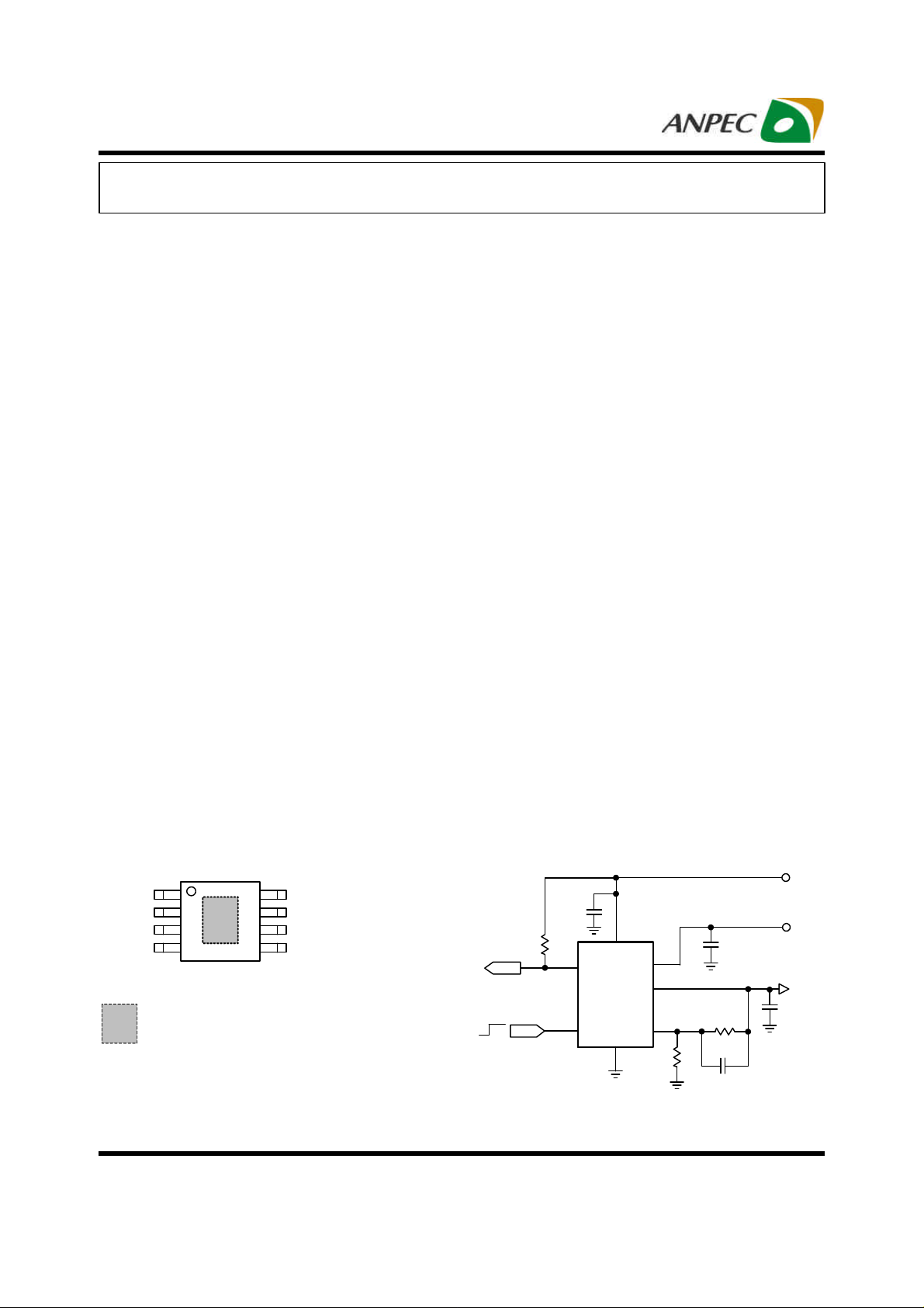
Simplified Application CircuitPin Configuration
V
1
GND
2
FB
3
VOUT
4
VOUT
SOP-8P (Top View)
= Exposed Pad
(connected to VIN plane for better heat dissipation)
ANPEC reserves the right to make changes to improve reliability or manufacturability without notice, and
advise customers to obtain the latest version of relevant information to verify before placing orders.
Copyright ANPEC Electronics Corp.
Rev. A.4 - Sep., 2009
8
7
6
5
EN
POK
VCNTL
VIN
POK
Enable
EN
VCNTL
POK
VOUT
APL5930
EN
GND
VIN
FB
Optional
www.anpec.com.tw1
CNTL
V
IN
V
OUT
APL5930
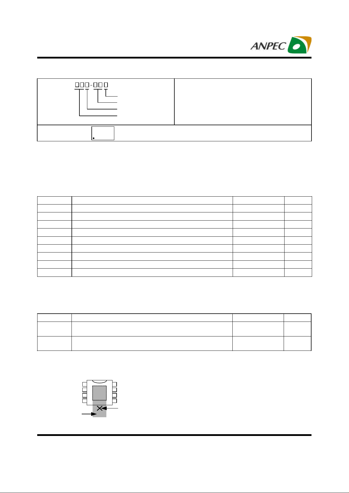
Ordering and Marking Information
APL5930
Assembly Material
Handling Code
Temperature Range
Package Code
APL5930 KA :
APL5930
XXXXX
Note: ANPEC lead-free products contain molding compounds/die attach materials and 100% matte tin plate termination finish; which
are fully compliant with RoHS. ANPEC lead-free products meet or exceed the lead-free requirements of IPC/JEDEC J-STD-020D for
MSL classification at lead-free peak reflow temperature. ANPEC defines “Green” to mean lead-free (RoHS compliant) and halogen
free (Br or Cl does not exceed 900ppm by weight in homogeneous material and total of Br and Cl does not exceed 1500ppm by
weight).
Absolute Maximum Ratings (Note 1)
Symbol Parameter Rating Unit
VIN VIN Supply Voltage (VIN to GND) -0.3 ~ 4.0 V
V
VCNTL Supply Voltage (VCNTL to GND) -0.3 ~ 7 V
CNTL
V
VOUT to GND Voltage -0.3 ~ VIN +0.3 V
OUT
POK to GND Voltage -0.3 ~ 7 V
EN, FB to GND Voltage -0.3 ~ V
PD Power Dissipation 3 W
TJ Maximum Junction Temperature 150
T
Storage Temperature -65 ~ 150
STG
T
Maximum Lead Soldering Temperature, 10 Seconds 260
SDR
Note 1: Absolute Maximum Ratings are those values beyond which the life of a device may be impaired. Exposure to absolute
maximum rating conditions for extended periods may affect device reliability.
Package Code
KA : SOP-8P
Operating Ambient Temperature Range
I : -40 to 85 oC
Handling Code
TR : Tape & Reel
Assembly Material
G : Halogen and Lead Free Device
XXXXX - Date Code
CNTL
+0.3 V
o
o
o
C
C
C
Thermal Characteristics
Symbol Parameter Typical Value Unit
θJA
θJC
Note 2: θJA is measured with the component mounted on a high effective thermal conductivity test board in free air. The exposed pad
Junction-to-Ambient Resistance in Free Air
Junction-to-Case Resistance in Free Air
of SOP-8P is soldered directly on the PCB.
Note 3: The “Thermal Pad Temperature” is measured on the PCB copper area connected to the thermal pad of package.
1
2
VIN
3
4
8
7
6
5
Measured Point
PCB Copper
Copyright ANPEC Electronics C orp.
Rev. A.4 - Sep., 2009
(Note 2)
(Note 3)
SOP-8P
SOP-8P
42
18
o
C/W
o
C/W
www.anpec.com.tw2
APL5930
Recommended Operating Conditions
Symbol Parameter Range Unit
V
VCNTL Supply Voltage 3.0 ~ 5.5 V
CNTL
VIN VIN Supply Voltage 1.2 ~ 3.65 V
V
VOUT Output Voltage (when V
OUT
I
VOUT Output Current
OUT
C
VOUT Output Capacitance
OUT
ESR
ESR of VOUT Output Capacitor
COUT
CNTL-VOUT
TA Ambient Temperature -40 ~ 85
TJ Junction Temperature -40 ~ 125
Electrical Characteristics
Unless otherwise specified, these specifications apply over V
are at TA=25oC.
>1.9V) 0.8 ~ VIN – V
Continuous Current 0 ~ 3
Peak Current 0 ~ 4
I
= 3A at 25% nominal V
OUT
I
= 2A at 25% nominal V
OUT
I
= 1A at 25% nominal V
OUT
8 ~ 1100
OUT
8 ~ 1700
OUT
8 ~ 2400
OUT
0 ~ 200
=5V, VIN=1.8V, V
CNTL
= 1.2V and TA= -40 ~ 85 oC. Typical values
OUT
V
DROP
A
µF
mΩ
o
C
o
C
Symbol Parameter Test Conditions
APL5930
Min. Typ. Max.
SUPPLY CURRENT
I
VCNTL Supply Current EN = VCNTL, I
VCNTL
=0A - 1.0 1.5 mA
OUT
ISD VCNTL Supply Current at Shutdown EN = GND - 15 30
VIN Supply Current at Shutdown EN = GND, VIN=3.65V - - 1
POWER-ON-RESET (POR)
Rising VCNTL POR Threshold 2.5 2.7 2.9 V
VCNTL POR Hysteresis - 0.4 - V
Rising VIN POR Threshold
VIN POR Hysteresis
0.8 0.9 1.0 V
- 0.5 - V
OUTPUT VOLTAGE
V
Reference Voltage FB=VOUT - 0.8 - V
REF
V
=3.0 ~ 5.5V, I
Output Voltage Accuracy
Load Regulation I
Line Regulation I
VOUT Pull-low Resistance
CNTL
TJ= -40~125oC
=0A ~3A - 0.06 0.25
OUT
=10mA, V
OUT
V
=3.3V, VEN=0V, V
CNTL
FB Input Current VFB=0.8V -100
= 0~3A,
OUT
= 3.0 ~ 5.5V - 0.15 - + 0.15 %/V
CNTL
<0.8V
OUT
-1.5
- +1.5 %
- 85 -
- 100
DROPOUT VOLTAGE
TJ=25oC - 0.26 0.31
TJ=-40~125oC - - 0.42
TJ=25oC - 0.24 0.29
TJ=-40~125oC - - 0.40
TJ=25oC - 0.23 0.28
TJ=-40~125oC - - 0.38
V
VIN-to-VOUT Dropout Voltage
DROP
V
=2.5V
OUT
V
V
OUT
OUT
=1.8V
=1.2V
V
=5.0V
CNTL
, I
=3A
OUT
Unit
µA
µA
%
Ω
nA
V
Copyright ANPEC Electronics C orp.
www.anpec.com.tw3
Rev. A.4 - Sep., 2009
APL5930
Electrical Characteristics (Cont.)
Unless otherwise specified, these specifications apply over V
are at TA=25oC.
Symbol
Parameter Test Conditions
DROPOUT VOLTAGE (CONT.)
I
Current-Limit Level
LIM
TJ=25oC 4.7 5.7 6.7
TJ= -40 ~ 125oC 4.2 - -
PROTECTIONS
I
Short Current-Limit Level VFB<0.2V - 1.1 - A
SHORT
Short Current-Limit Blanking
Time
From beginning of soft-start 0.6 1.5 - ms
TSD Thermal Shutdown Temperature TJ rising - 170 -
Thermal Shutdown Hysteresis - 50 -
ENABLE AND SOFT-START
EN Logic High Threshold
Voltage
VEN rising 0.5 0.8 1.1 V
EN Hysteresis - 0.1 - V
EN Pull-High Current EN=GND - 5 -
TSS Soft-Start Interval 0.3 0.6 1.2 ms
Turn On Delay From being enabled to V
POWER-OK AND DELAY
V
Rising POK Threshold Voltage VFB rising 90 92 94 %
THPOK
POK Threshold Hysteresis - 8 - %
POK Pull-low Voltage POK sinks 5mA - 0.25 0.4 V
POK Debounce Interval VFB<falling POK voltage threshold - 10 POK Delay Time From VFB =V
=5V, VIN=1.8V, V
CNTL
rising 10% 60 120 180
OUT
to rising edge of the V
THPOK
= 1.2V and TA= -40 ~ 85 oC. Typical values
OUT
APL5930
Min. Typ. Max.
POK
1 2 4 ms
Unit
A
o
C
o
C
µA
µs
µs
Copyright ANPEC Electronics C orp.
www.anpec.com.tw4
Rev. A.4 - Sep., 2009
APL5930
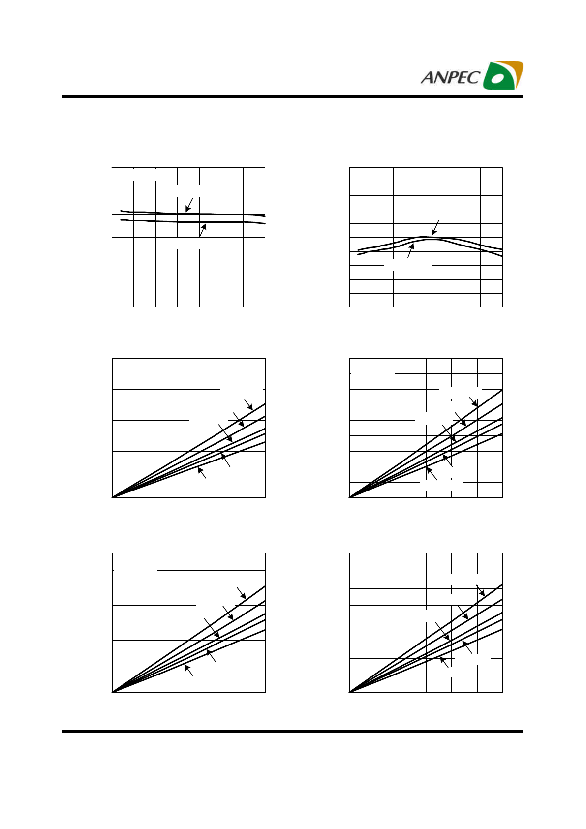
Typical Operating Characteristics
Current-Limit vs. Junction
Temperature
6.5
V
= 1.2V
OUT
6.0
(A)
5.5
LIM
5.0
4.5
V
CNTL
V
CNTL
= 5V
= 3.3V
Current-Limit, I
4.0
3.5
-50 -25 0 25 50 75 100 125
Junction Temperature (
Dropout Voltage vs. Output Current
450
V
= 5V
CNTL
400
V
= 1.2V
OUT
350
(mV)
300
DROP
250
200
150
100
Dropout Voltage, V
50
0
0 0.5 1 1.5 2 2.5 3
Output Current, I
TJ = 75°C
TJ = 25°C
TJ = - 40°C
OUT
Dropout Voltage vs. Output Current
400
V
= 5V
CNTL
350
V
= 1.5V
OUT
300
(mV)
DROP
250
200
TJ = 125°C
TJ = 75°C
TJ = 25°C
o
)
C
TJ = 125°C
TJ = 0°C
(A)
Short Current-Limit vs. Junction
Temperature
1.20
1.18
1.16
(mA)
1.14
SHORT
1.12
1.10
1.08
1.06
1.04
Short Current-Limit, I
1.02
1.00
-50 -25 0 25 50 75 100
V
CNTL
= 3.3V
V
CNTL
= 5V
Junction Temperature (
Droput Voltage vs. Output Current
450
V
= 3.3V
CNTL
400
V
= 1.2V
OUT
350
(mV)
300
DROP
250
200
150
100
Dropout Voltage, V
50
0
0 0.5 1 1.5 2 2.5 3
Output Current, I
TJ = 125°C
TJ = 75°C
TJ = 25°C
TJ = 0°C
TJ = - 40°C
OUT
Dropout Voltage vs. Output Current
400
V
= 5V
CNTL
350
V
= 1.8V
OUT
300
(mV)
DROP
250
200
TJ = 75°C
TJ = 25°C
o
)
C
(A)
TJ = 125°C
125
150
100
Dropout Voltage, V
50
0
0 0.5 1 1.5 2 2.5 3
Output Current, I
TJ = 0°C
TJ = - 40°C
OUT
Copyright ANPEC Electronics C orp.
Rev. A.4 - Sep., 2009
(A)
150
100
Dropout Voltage, V
50
0
0 0.5 1 1.5 2 2.5 3
Output Current, I
TJ = - 40°C
OUT
www.anpec.com.tw5
TJ = 0°C
(A)
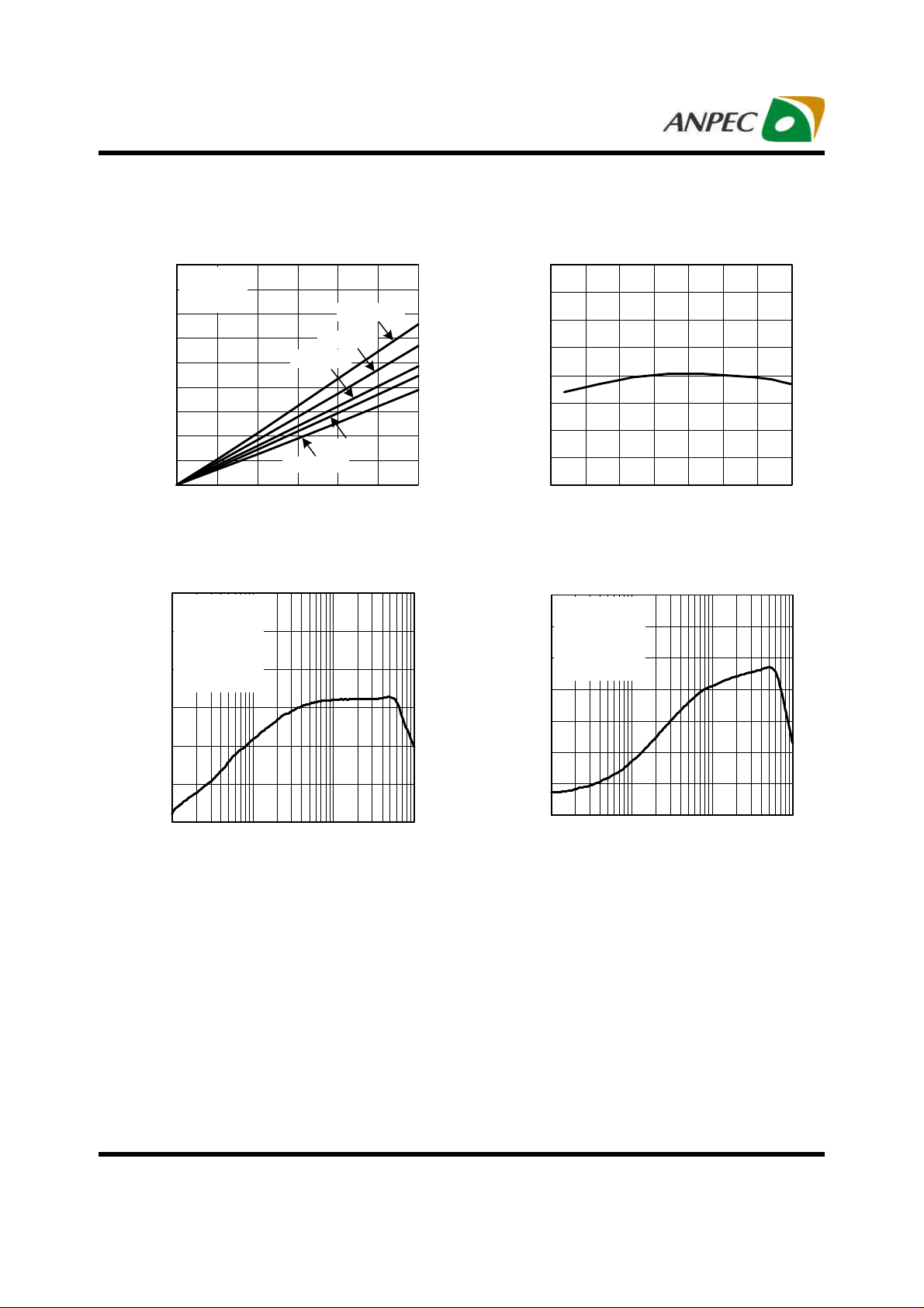
APL5930
Typical Operating Characteristics (Cont.)
Dropout Voltage vs. Output Current
450
V
= 5V
CNTL
400
V
= 2.5V
OUT
350
(mV)
300
DROP
250
200
150
100
Dropout Voltage, V
50
0
0 0.5 1 1.5 2 2.5 3
TJ = 25°C
TJ = - 40°C
Output Current, I
TJ = 125°C
TJ = 75°C
TJ = 0°C
(A)
OUT
VIN Power Supply Rejection Ratio
(PSRR)
0
V
=5V
CNTL
VIN=1.8V
-10
V
=100mV
PK-PK
IN
V
=1.2V
OUT
I
=3A
OUT
-20
CIN=10µF
C
=10µF
OUT
-30
-40
-50
Power Supply Rejection Ratio (dB)
-60
1000 10000 100000 1000000
Frequency (Hz)
Reference Voltage vs. Junction
Temperature
0.808
0.806
(V)
0.804
REF
0.802
0.800
0.798
0.796
Reference Voltage, V
0.794
0.792
-50 -25 0 25 50 75 100 125
Junction Temperature (oC)
VCNTL Power Supply Rejection Ratio
(PSRR)
0
V
=4.6~5.4V
CNTL
VIN=1.8V
-10
V
=1.2V
OUT
I
=3A
OUT
-20
CIN=C
=10µF
OUT
-30
-40
-50
-60
Power Supply Rejection Ratio (dB)
-70
1000 10000 100000 1000000
Frequency (Hz)
Copyright ANPEC Electronics C orp.
Rev. A.4 - Sep., 2009
www.anpec.com.tw6

APL5930
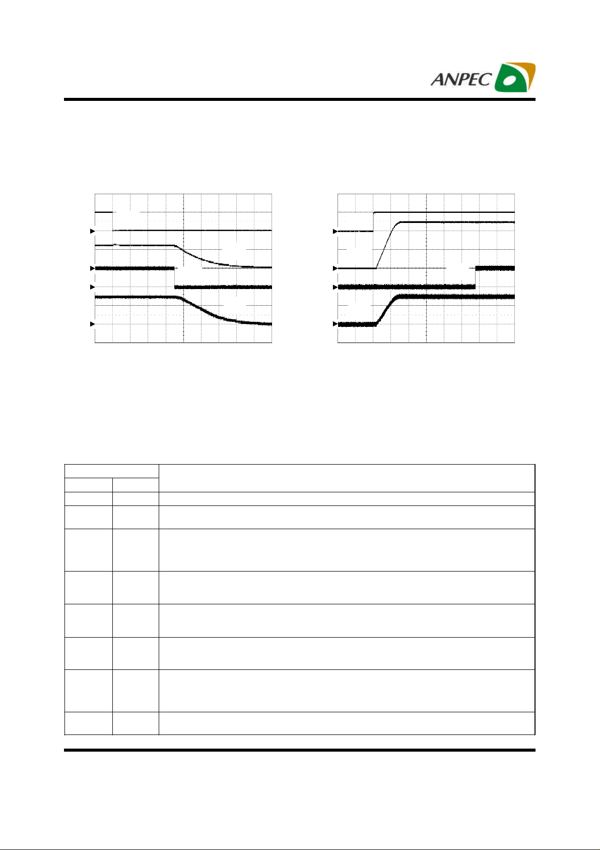
Operating Waveforms
Refer to the typical application circuit. The test condition is VIN=1.8V, V
unless otherwise specified.
CNTL
=5V, V
=1.2V, TA= 25oC
OUT
1
2
3
4
C
=10µF, CIN=10µF, RL=0.4Ω
OUT
CH1: V
CNTL
CH2: VIN, 1V/Div, DC
CH3: V
CH4: V
TIME: 2ms/Div
, 1V/Div, DC
OUT
, 5V/Div, DC
POK
Load Transient Response
Power On
, 5V/Div, DC
Power Off
V
CNTL
V
CNTL
V
IN
V
OUT
V
POK
1
2
3
4
C
=10µF, CIN=10µF, RL=0.4Ω
OUT
CH1: V
CNTL
CH2: VIN, 1V/Div, DC
CH3: V
CH4: V
TIME: 2ms/Div
, 1V/Div, DC
OUT
, 5V/Div, DC
POK
, 5V/Div, DC
V
IN
V
OUT
V
POK
Over Current Protection
V
1
2
I
=10mA to 3A to 10mA (rise / fall time = 1µs)
OUT
C
=10µF, CIN=10µF
OUT
CH1: V
OUT
CH2: I
, 1A/Div, DC
OUT
OUT
I
OUT
, 50mV/Div, AC
TIME: 50µs/Div
Copyright ANPEC Electronics C orp.
Rev. A.4 - Sep., 2009
1
4
C
=10µF, CIN=10µF, I
OUT
CH1: V
CH4: I
OUT
TIME: 0.2ms/Div
V
OUT
I
OUT
, 0.5V/Div, DC
OUT
, 2A/Div, DC
= 2A to 5.6A
OUT
www.anpec.com.tw7
APL5930
Operating Waveforms (Cont.)
Refer to the typical application circuit. The test condition is VIN=1.8V, V
unless otherwise specified.
CNTL
=5V, V
=1.2V, TA= 25oC
OUT
Shutdown
V
1
2
3
4
EN
C
=10µF, CIN=10µF, RL=0.4Ω
OUT
CH1: VEN, 5V/Div, DC
CH2: V
CH3: V
CH4: I
TIME: 2µs/Div
, 1V/Div, DC
OUT
, 5V/Div, DC
POK
, 2A/Div, DC
OUT
Pin Description
Enable
V
EN
1
V
OUT
V
POK
I
OUT
V
OUT
2
3
I
OUT
4
C
=10µF, CIN=10µF, RL=0.4Ω
OUT
CH1: VEN, 5V/Div, DC
CH2: V
CH3: V
CH4: I
TIME: 0.5ms/Div
, 0.5V/Div, DC
OUT
, 5V/Div, DC
POK
, 2A/Div, DC
OUT
V
POK
PIN
NO. NAME
FUNCTION
1 GND Ground pin of the circuitry. All voltage levels are measured with respect to this pin.
2 FB
Voltage Feedback Pin. Connecting this pin to an external resistor divider receives the feedback voltage
of the regulator.
Output pin of the regulator. Connecting this pin to load and output capacitors (10µF at least) is required
3,4
VOUT
for stability and improving transient response. The output voltage is programmed by the resistor-divider
connected to FB pin. The VOUT can provide 3A (max.) load current to loads. During shutdown, the
output voltage is quickly discharged by an internal pull-low MOSFET.
Main supply input pin for voltage conversions. A decoupling capacitor (≥10µF recommended) is usually
5 VIN
connected near this pin to filter the voltage noise and improve transient response. The voltage on this
pin is monitored for Power-On-Reset purpose.
Bias voltage input pin for internal control circuitry. Connect this pin to a voltage source (+5V
6 VCNTL
recommended). A decoupling capacitor (1µF typical) is usually connected near this pin to filter the
voltage noise. The voltage at this pin is monitored for Power-On-Reset purpose.
Power-OK signal output pin. This pin is an open-drain output used to indicate the status of output
7 POK
voltage by sensing FB voltage. This pin is pulled low when output voltage is not within the Power-OK
voltage window.
Active-high enable control pin. Applying and holding the voltage on this pin below the enable voltage
8 EN
threshold shuts down the output. When re-enabled, the IC undergoes a new soft-start process. When
leave this pin open, an internal pull-up current (5µA typical) pulls the EN voltage and enables the
regulator.
Exposed
Pad
-
Connect this pad to system VIN plane for good thermal conductivity.
Copyright ANPEC Electronics C orp.
Rev. A.4 - Sep., 2009
www.anpec.com.tw8

APL5930
Block Diagram
VCNTL
VCNTL
5µA
EN
0.8V
POK
PWOK
Delay
Typical Application Circuit
C
CNTL
1µF
R3
5.1kΩ
POK
EN
Enable
7
POK
APL5930
8
EN
Thermal
Shutdown
Enable
POR
90%
V
6
VCNTL
VOUT
GND
1
V
0.8V
REF
VIN
REF
FB
Control Logic
and
Soft-Start
Soft-Start
Error Amplifier
FB
5
3,4
2
R2
24kΩ
POR
Enable
Current-Limit
and
Short Current-
Limit
R1
12kΩ
Power-
On-Reset
(POR)
ISEN
C
IN
10µF
VIN
VOUT
GND
V
CNTL
(+5V is preferred)
V
IN
+1.8V
V
OUT
+1.2V / 3A
C
OUT
10µF
(X5R/X7R Recommended)
Copyright ANPEC Electronics C orp.
Rev. A.4 - Sep., 2009
Optional
(X5R/X7R Recommended)
10µF: GRM31MR60J106KE19 Murata
C1
www.anpec.com.tw9

APL5930
Function Description
Power-On-Reset
A Power-On-Reset (POR) circuit monitors both of supply
voltages on VCNTL and VIN pins to prevent wrong logic
controls. The POR function initiates a soft-start process
after both of the supply voltages exceed their rising POR
voltage thresholds during powering on. The POR function also pulls low the POK voltage regardless the output
status when one of the supply voltages falls below its
falling POR voltage threshold.
Internal Soft-Start
An internal soft-start function controls rise rate of the output voltage to limit the current surge during start-up. The
typical soft-start interval is about 0.6 ms.
Output Voltage Regulation
An error amplifier works with a temperature-compensated 0.8V reference and an output NMOS regulates
output to the preset voltage. The error amplifier is designed with high bandwidth and DC gain provides very
fast transient response and less load regulation. It compares the reference with the feedback voltage and amplifies the difference to drive the output NMOS which provides load current from VIN to VOUT.
Thermal Shutdown
A thermal shutdown circuit limits the junction temperature of APL5930. When the junction temperature exceeds
+170oC, a thermal sensor turns off the output NMOS, allowing the device to cool down. The regulator regulates
the output again through initiation of a new soft-start process after the junction temperature cools by 50oC, resulting in a pulsed output during continuous thermal overload conditions. The thermal shutdown is designed with
a 50oC hysteresis to lower the average junction temperature during continuous thermal overload conditions, extending lifetime of the device.
For normal operation, the device power dissipation should
be externally limited so that junction temperatures will
not exceed +125oC.
Enable Control
The APL5930 has a dedicated enable pin (EN). A logic
low signal applied to this pin shuts down the output. Following a shutdown, a logic high signal re-enables the
output through initiation of a new soft-start cycle. When
left open, this pin is pulled up by an internal current source
(5µA typical) to enable normal operation. It’s not necessary to use an external transistor to save cost.
Current-Limit Protection
The APL5930 monitors the current flowing through the
output NMOS and limits the maximum current to prevent
load and APL5930 from damages during current overload conditions.
Short Current-Limit Protection
The short current-limit function reduces the current-limit
level down to 1.1A (typical) when the voltage on FB pin
falls below 0.2V (typical) during current overload or shortcircuit conditions.
The short current-limit function is disabled for successful start-up during soft-start interval.
Copyright ANPEC Electronics C orp.
Rev. A.4 - Sep., 2009
Power-OK and Delay
The APL5930 indicates the status of the output voltage by
monitoring the feedback voltage (VFB) on FB pin. As the
VFB rises and reaches the rising Power-OK voltage threshold (V
the end of the delay time, the IC turns off the internal
NMOS of the POK to indicate that the output is ok. As the
VFB falls and reaches the falling Power-OK voltage
threshold, the IC turns on the NMOS of the POK (after a
debounce time of 10µs typical).
), an internal delay function starts to work. At
THPOK
www.anpec.com.tw10

APL5930
Application Information
Power Sequencing
The power sequencing of VIN and VCNTL is not necessary to be concerned. However, do not apply a voltage to
VOUT for a long time when the main voltage applied at
VIN is not present. The reason is the internal parasitic
diode from VOUT to VIN conducts and dissipates power
without protections due to the forward-voltage.
Output Capacitor
The APL5930 requires a proper output capacitor to maintain stability and improve transient response. The output
capacitor selection is dependent upon ESR (equivalent
series resistance) and capacitance of the output capacitor over the operating temperature.
Ultra-low-ESR capacitors (such as ceramic chip
capacitors) and low-ESR bulk capacitors (such as solid
tantalum, POSCap, and Aluminum electrolytic capacitors)
can all be used as output capacitors.
During load transients, the output capacitors, depending
on the stepping amplitude and slew rate of load current,
are used to reduce the slew rate of the current seen by
the APL5930 and help the device to minimize the variations of output voltage for good transient response. For
the applications with large stepping load current, the lowESR bulk capacitors are normally recommended.
Decoupling ceramic capacitors must be placed at the
load and ground pins as close as possible and the impedance of the layout must be minimized.
Ultra-low-ESR capacitors (such as ceramic chip capacitors) and low-ESR bulk capacitors (such as solid
tantalum, POSCap, and Aluminum electrolytic capacitors)
can all be used as an input capacitor of VIN. For most
applications, the recommended input capacitance of VIN
is 10µF at least. However, if the drop of the input voltage
is not cared, the input capacitance can be less than 10µF.
More capacitance reduces the variations of the supply
voltage on VIN pin.
Setting Output Voltage
The output voltage is programmed by the resistor divider
connected to FB pin. The preset output voltage is calculated by the following equation :
R1
+⋅=
10.8 VOUT
R2
........... (V)
Where R1 is the resistor connected from VOUT to FB with
Kelvin sensing connection and R2 is the resistor connected from FB to GND. A bypass capacitor(C1) may be
connected with R1 in parallel to improve load transient
response and stability.
Input Capacitor
The APL5930 requires proper input capacitors to supply
current surge during stepping load transients to prevent
the input voltage rail from dropping. Because the parasitic inductor from the voltage sources or other bulk capacitors to the VIN pin limit the slew rate of the surge
currents, more parasitic inductance needs more input
capacitance.
Copyright ANPEC Electronics C orp.
Rev. A.4 - Sep., 2009
www.anpec.com.tw11
APL5930
Layout Consideration
the top-layer of PCBs. The VIN pad must have wide
size to conduct heat into the ambient air through the
VIN plane and PCB as a heat sink.
2. Please place the input capacitors for VIN and VCNTL
pins near the pins as close as possible for
decoupling high-frequency ripples.
3. Ceramic decoupling capacitors for load must be
placed near the load as close as possible for
decoupling high-frequency ripples.
4. To place APL5930 and output capacitors near the
load reduces parasitic resistance and inductance
for excellent load transient response.
5. The negative pins of the input and output capacitors
and the GND pin must be connected to the ground
plane of the load.
6. Large current paths, shown by bold lines on the figure 1, must have wide tracks.
7. Place the R1, R2, and C1 near the APL5930 as close
as possible to avoid noise coupling.
8. Connect the ground of the R2 to the GND pin by using a dedicated track.
9. Connect the one pin of the R1 to the load for Kelvin
sensing.
10. Connect one pin of the C1 to the VOUT pin for reliable feedback compensation.
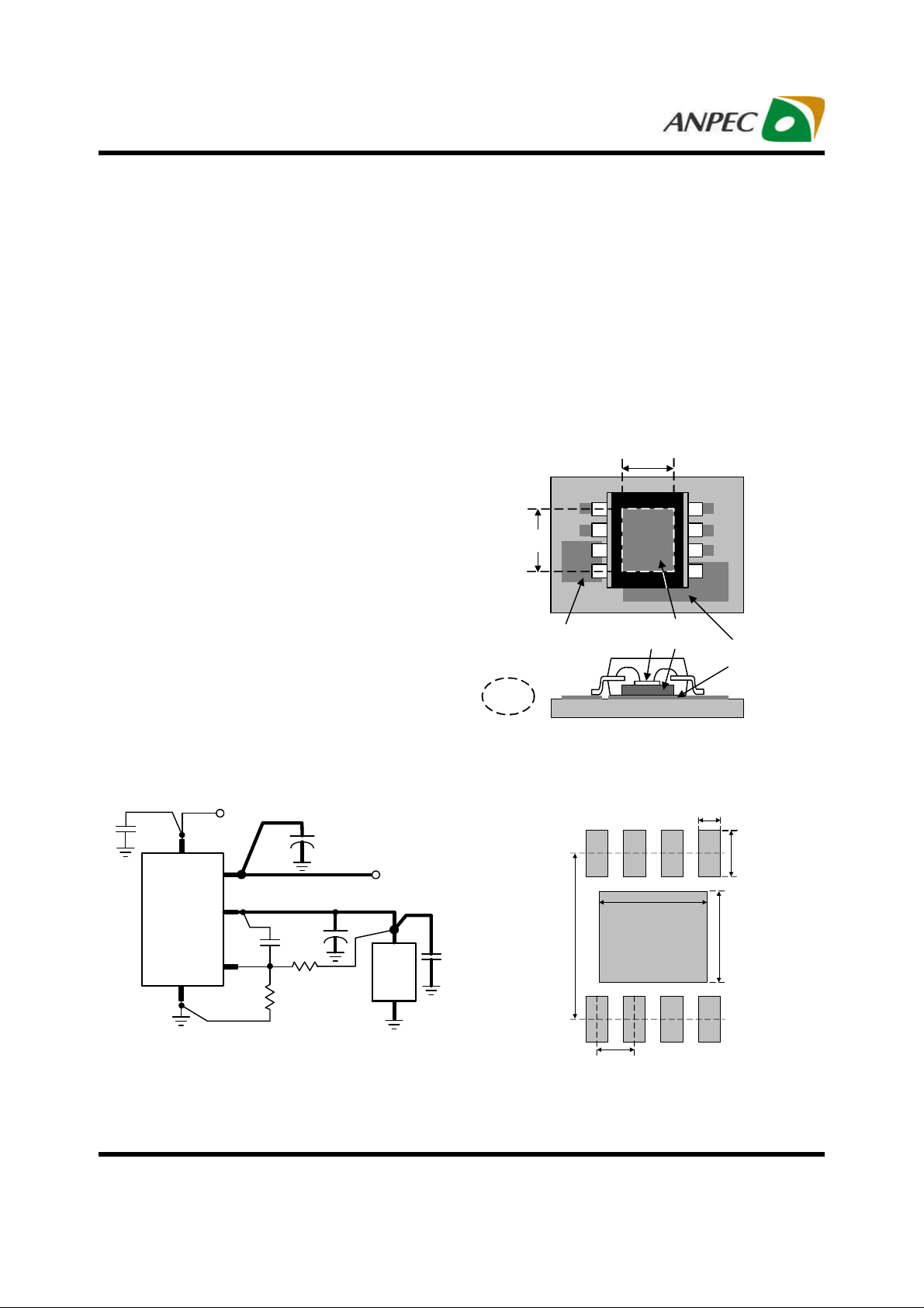
Thermal Consideration1. Please solder the Exposed Pad on the VIN pad on
Refer to the figure 2, the SOP-8P is a cost-effective pack-
age featuring a small size like a standard SOP-8 and a
bottom exposed pad to minimize the thermal resistance
of the package, being applicable to high current applications. The exposed pad must be soldered to the top-layer
VIN plane. The copper of the VIN plane on the Top layer
conducts heat into the PCB and ambient air. Please enlarge the area of the top-layer pad and the VIN plane to
reduce the case-to-ambient resistance (θCA).
102 mil
Ambient
Air
118 mil
Top
VOUT
plane
1
2
3
4
SOP-8P
Die
8
7
6
5
Exposed
Pad
PCB
Top
VIN
plane
Figure 2
V
CNTL
C
CNTL
VCNTL
APL5930
GND
VIN
VOUT
C1
FB
R2
C
IN
C
OUT
R1
Figure 1
Copyright ANPEC Electronics C orp.
Rev. A.4 - Sep., 2009
V
V
OUT
Load
Recommended Minimum Footprint
0.024
8 7 6 5
IN
0.138
0.212
1 2 3 4
0.050
Unit : Inch
0.072
0.118
www.anpec.com.tw12

APL5930
Pack age Information
SOP-8P
D
D1
SEE VIEW A
L
b
c
D
E
e
h
A
A1
A2
D1
E1
0
THERMAL
PAD
e
S
Y
M
B
O
L
MIN.
0.00
1.25
0.31
0.17
4.80 5.00
2.50
5.80 6.20
3.80 4.00
2.00
0.25
0.40
E2
b
MILLIMETERS
1.27 BSC
0oC
E
E1
o
h X 45
c
A
A2
0.25
A1
L
VIEW A
SOP-8P
MAX.
1.60
0.15
0.51
0.25
3.50
3.00
0.50
1.27
8oC 0oC 8oC
MIN.
0.000
0.049
0.012
0.007
0.189 0.197
0.098
0.228 0.244
0.150 0.157
0.079E2
0.010
0.016
θ
INCHES
0.050 BSC
GAUGE PLANE
SEATING PLANE
MAX.
0.063
0.006
0.020
0.010
0.138
0.118
0.020
0.050
Note : 1. Followed from JEDEC MS-012 BA.
2. Dimension "D" does not include mold flash, protrusions or gate burrs.
Mold flash, protrusion or gate burrs shall not exceed 6 mil per side .
3. Dimension "E" does not include inter-lead flash or protrusions.
Inter-lead flash and protrusions shall not exceed 10 mil per side.
Copyright ANPEC Electronics C orp.
Rev. A.4 - Sep., 2009
www.anpec.com.tw13

APL5930
Carrier Tape & R eel Dimensions
OD0
B0
P0
P2
P1
A
E1
F
W
Application
SOP-8P
K0
SECTION A-A
B
A
H
A0
SECTION B-B
OD1
B
T
A
d
T1
A H T1 C d D W E1 F
330.0±2.00 50 MIN.
12.4+2.00
-0.00
13.0+0.50
-0.20
1.5 MIN. 20.2 MIN. 12.0±0.30 1.75±0.10 5.5±0.05
P0 P1 P2 D0 D1 T A0 B0 K0
4.0±0.10 8.0±0.10 2.0±0.05
1.5+0.10
-0.00
1.5 MIN.
0.6+0.00
-0.40
6.40±0.20 5.20±0.20 2.10±0.20
Devices Per Unit
Package Type
SOP- 8P
Copyright ANPEC Electronics C orp.
Rev. A.4 - Sep., 2009
(mm)
Unit Quantity
Tape & Reel 2500
www.anpec.com.tw14

APL5930
Taping Direction Information
SOP-8P
USER DIRECTION OF FEED
Classification Profile
Copyright ANPEC Electronics C orp.
Rev. A.4 - Sep., 2009
www.anpec.com.tw15

APL5930
Classification Reflow Profiles
Profile Feature Sn-Pb Eutectic Assembly Pb-Free Assembly
Preheat & Soak
Temperature min (T
Temperature max (T
Time (T
smin
to T
smax
smin
smax
) (ts)
)
)
Average ramp-up rate
(T
to TP)
smax
Liquidous temperature (TL)
Time at liquidous (tL)
Peak package body Temperature
(Tp)*
Time (tP)** within 5°C of the specified
classification temperature (Tc)
Average ramp-down rate (Tp to T
smax
Time 25°C to peak temperature
See Classification Temp in table 1 See Classification Temp in table 2
)
100 °C
150 °C
60-120 seconds
150 °C
200 °C
60-120 seconds
3 °C/second max. 3°C/second max.
183 °C
60-150 seconds
217 °C
60-150 seconds
20** seconds 30** seconds
6 °C/second max. 6 °C/second max.
6 minutes max. 8 minutes max.
* Tolerance for peak profile Temperature (Tp) is defined as a supplier minimum and a user maximum.
** Tolerance for time at peak profile temperature (tp) is defined as a supplier minimum and a user maximum.
Table 1. SnPb Eutectic Process – Classification Temperatures (Tc)
Package
Thickness
<2.5 mm
Volume mm
3
Volume mm
<350
235 °C 220 °C
≥350
3
≥2.5 mm 220 °C 220 °C
Table 2. Pb-free Process – Classification Temperatures (Tc)
Package
Thickness
<1.6 mm
1.6 mm – 2.5 mm
Volume mm3
<350
Volume mm3
350-2000
Volume mm3
260 °C 260 °C 260 °C
260 °C 250 °C 245 °C
>2000
≥2.5 mm 250 °C 245 °C 245 °C
Reliability Test Program
Test item Method Description
SOLDERABILITY JESD-22, B102
HOLT JESD-22, A108
PCT JESD-22, A102
TCT JESD-22, A104
HBM MIL-STD-883-3015.7
MM JESD-22, A115
Latch-Up JESD 78
Copyright ANPEC Electronics C orp.
Rev. A.4 - Sep., 2009
5 Sec, 245°C
1000 Hrs, Bias @ 125°C
168 Hrs, 100%RH, 2atm, 121°C
500 Cycles, -65°C~150°C
VHBM≧2KV
VMM≧200V
10ms, 1tr≧100mA
www.anpec.com.tw16

APL5930
Customer Service
Anpec Electronics Corp.
Head Office :
No.6, Dusing 1st Road, SBIP,
Hsin-Chu, Taiwan, R.O.C.
Tel : 886-3-5642000
Fax : 886-3-5642050
Taipei Branch :
2F, No. 11, Lane 218, Sec 2 Jhongsing Rd.,
Sindian City, Taipei County 23146, Taiwan
Tel : 886-2-2910-3838
Fax : 886-2-2917-3838
Copyright ANPEC Electronics C orp.
Rev. A.4 - Sep., 2009
www.anpec.com.tw17

 Loading...