Anpec APL5913KA Schematics

APL5913
0.8V Reference Ultra Low Dropout (0.25V@3A) Linear Regulator
Features
• Ultra Low Dropout
- 0.25V(typical) at 3A Output Current
• Low ESR Output Capacitor (Multi-layer Chip
Capacitors (MLCC)) Applicable
• 0.8V Reference Voltage
• High Output Accuracy
- ±1.5% over Line, Load and Temperature
• Fast Transient Response
• Adjustable Output Voltage by External
Resistors
• Power-On-Reset Monitoring on Both VCNTL and
VIN Pins
• Internal Soft-Start
• Current-Limit Protection
• Under-Voltage Protection
• Thermal Shutdown with Hysteresis
• Power-OK Output with a Delay Time
• Shutdown for Standby or Suspend Mode
• Simple SOP-8P Package with Exposed Pad
• Lead Free and Green Devices Available
(RoHS Compliant)
General Description
The APL5913 is a 3A ultra low dropout linear regulator.
This product is specifically designed to provide well supply v olatage for front-side-bus termination on
motherboards and NB applications. The IC needs two
supply voltages, a control voltage for the c ircuitry and a
main supply voltage for power c onversion, to reduce
power diss ipation and provide extremely low dropout.
The APL5913 integrates many functions. A Power-On-Reset (POR) circuit monitors both s upply voltages to prevent wrong operations. A thermal s hutdown and current
limit functions protect the device against thermal and current over-loads. A POK indicates the output status with
time delay which is set internally. It can control other converter for power sequence. The APL5913 is enabled by
other power sys tem. Pulling and holding the EN pin below 0.3V shuts off the output.
The APL5913 is available in SOP-8P package which features small size as SOP-8 and an Exposed Pad to reduce
the junction-to-case resistance, being applicable in
2~2.4W applications.
Applications
• Front Side Bus VTT (1.2V/3A)
• Note Book PC Applications
• Motherboard Applications
Copyright ANPEC Electronics Corp.
Rev. A.7 - Apr., 2008
Pin Configuration
1
GND
2
FB
VOUT
VOUT
SOP-8P (Top View)
= Exposed Pad
(connected to VIN plane for better heat
dissipation)
VIN
3
4
8
7
6
5
EN
POK
VCNTL
VIN
www.anpec.com.tw1
APL5913
o
Ordering and Marking Information
APL5913
Assembly Material
Handling Code
Temperature Range
Package Code
Package Code
KA : SOP-8P
Operating Ambient Temperature Range
C : 0 to 70 C
Handing Code
TR : Tape & Reel
Assembly Material
L : Lead Free Device
G : Halogen and Lead Free Device
APL5913 KA :
APL5913
XXXXX
XXXXX - Date Code
Note: ANPEC lead-free products contain molding compounds/die attach materials and 100% matte tin plate termination finish; which
are fully compliant with RoHS. ANPEC lead-free products meet or exceed the lead-free requirements of IPC/JEDEC J-STD-020C for
MSL classification at lead-free peak reflow temperature. ANPEC defines “Green” to mean lead-free (RoHS compliant) and halogen
free (Br or Cl does not exceed 900ppm by weight in homogeneous material and total of Br and Cl does not exceed 1500ppm by
weight).
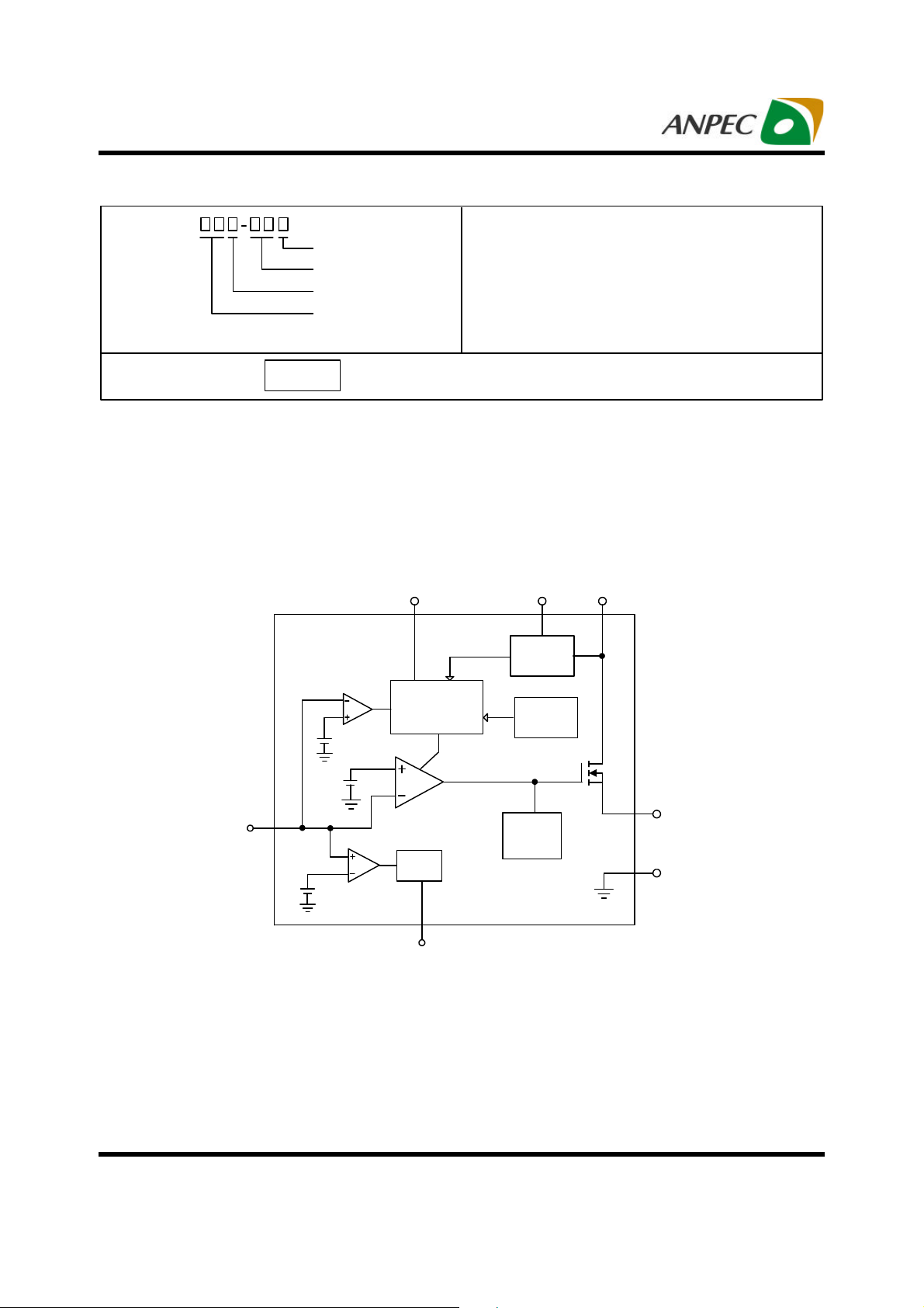
Block Diagram
EN
Power-
On-Reset
VINVCNTL
FB
VREF
0.8V
90%
VREF
0.4V
UV
POK
Soft-Start
and
Control Logic
EAMP
Delay
POK
Thermal
Limit
VOUT
Current
Limit
GND
Copyright ANPEC Electronics C orp.
www.anpec.com.tw2
Rev. A.7 - Apr., 2008
APL5913
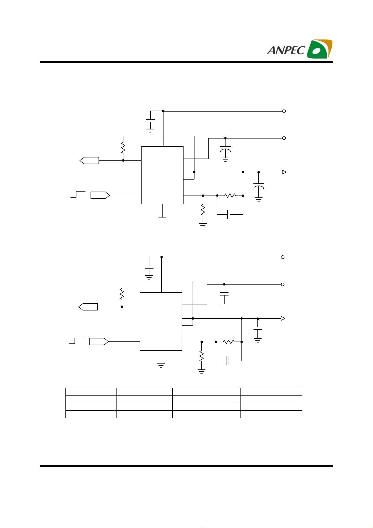
Typical Application Circuits
1. Using an Output Capacitor with ESR≥18mΩ
C
CNTL
1µF
Enable
POk
EN
R3
1k
7
8
VCNTL
POk
APL5913
EN
GND
1
6
VOUT
VOUT
VIN
FB
V
CNTL
+5V
V
IN
C
OUT
+1.5V
V
OUT
+1.2V / 3A
C
IN
5
100µF
3
4
2
220µF
R1
R2
1k
2k
C1
33nF (in the range of 12 ~ 48nF)
2. Using an MLCC as the Output Capacitor
C
CNTL
1µF
R3
1k
POk
EN
7
8
Enable
V
OUT
(V)
R1 (kΩ) R2 (kΩ)
1.05 43 137.6 47
1.5 27 30.86 82
1.8 15 12 150
POk
EN
6
VCNTL
APL5913
GND
1
VIN
VOUT
VOUT
FB
V
CNTL
+5V
V
IN
OUT
+1.5V
V
OUT
+1.2V / 3A
C
IN
5
22µF
3
4
C
2
22µF
R1
R2
39k
78k
C1
56pF
C1 (pF)
Copyright ANPEC Electronics C orp.
Rev. A.7 - Apr., 2008
www.anpec.com.tw3
APL5913
Absolute Maximum Ratings
Symbol Parameter Rating Unit
V
VCNTL Supply Voltage (VCNTL to GND) -0.3 ~ 7 V
CNTL
VIN VIN Supply Voltage (VIN to GND) -0.3 ~ 3.3 V
V
EN and FB to GND -0.3 ~ V
I/O
V
POK to GND -0.3 ~ 7 V
POK
PD Power Dissipation 3 W
TJ Junction Temperature 150
T
Storage Temperature -65 ~ 150
STG
T
Maximum Lead Soldering Temperature, 10 Seconds 260
SDR
Thermal Characteristics
Symbol Parameter Value Unit
θ
JA
θJC
Junction-to- Ambient Thermal Resistance in Free Air
Junction -to - Case Thermal Resistance in Free Air
(Note1)
42
(Note 2)
18
CNTL
+0.3
o
C/W
o
C/W
V
o
C
o
C
o
C
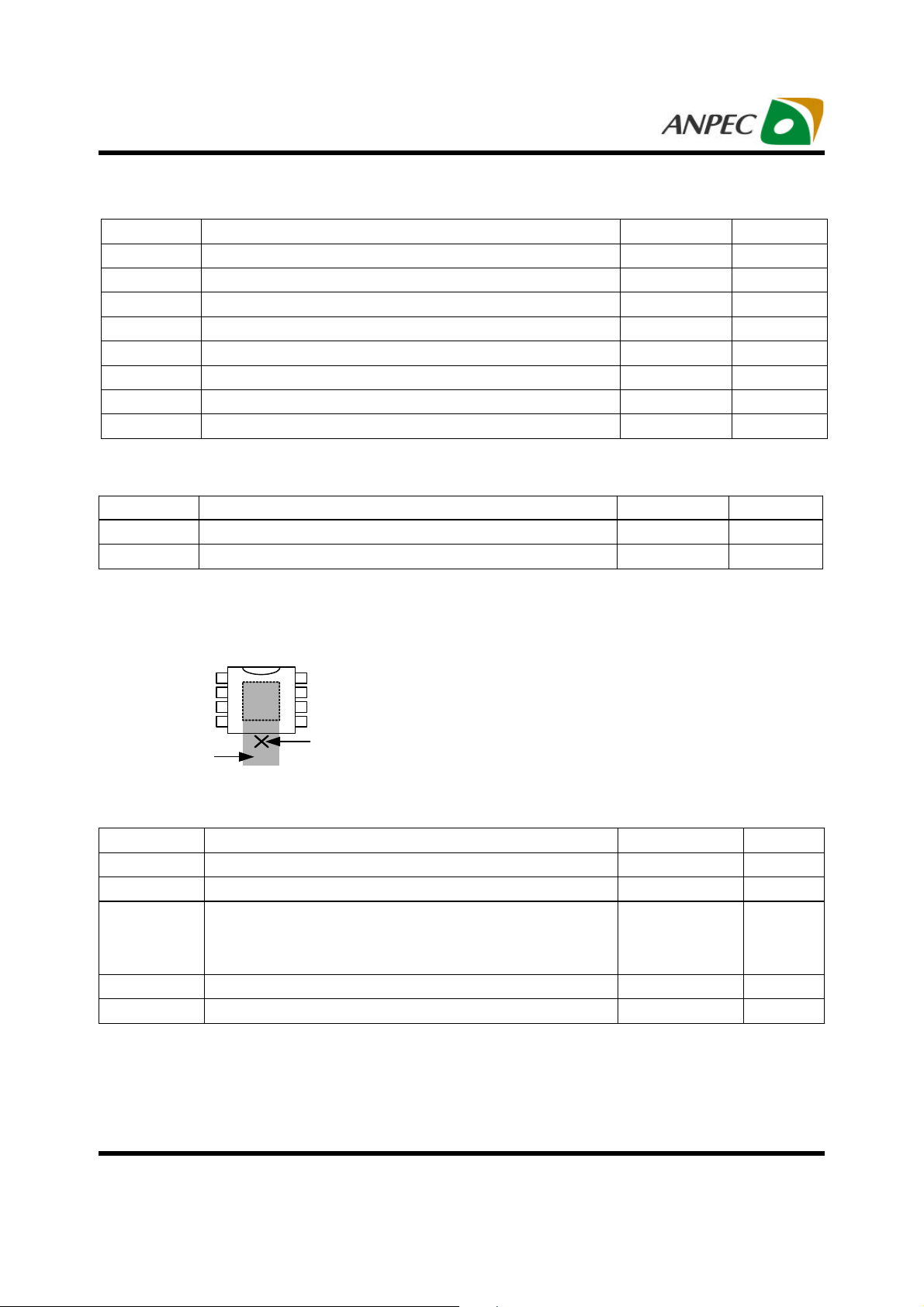
Note 1 : θJA is measured with the component mounted on a high effective thermal conductivity test board in free air. The exposed pad
of SOP-8P is soldered directly on the PCB.
Note 2 : The “Thermal Pad Temperature” is measured on the PCB copper area connected to the thermal pad of package.
1
2
VIN
3
4
8
7
6
5
Measured Point
PCB Copper
Recommended Operating Conditions
Symbol Parameter Range Unit
V
VCNTL Supply Voltage 3.1 ~ 6 V
CNTL
VIN VIN Supply Voltage 1.1 ~ 3.3 V
Output Voltage
V
OUT
I
VOUT Output Current 0 ~ 4 A
OUT
V
V
CNTL
CNTL
=3.3±5%
=5.0±5%
TJ Junction Temperature -25 ~ 125
0.8 ~ 1.2
0.8 ~ VIN-0.2
V
o
C
Copyright ANPEC Electronics C orp.
www.anpec.com.tw4
Rev. A.7 - Apr., 2008
APL5913
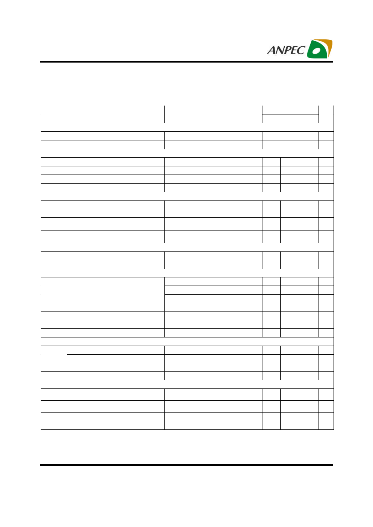
Electrical Characteristics
Refer to the typical application circuit. These specifications apply over, V
to 70°C, unless otherwise specified. Typical values refer to TA = 25°C.
= 5V, VIN = 1.5V, V
CNTL
= 1.2V and TA = 0
OUT
Symbol
Parameter Test Conditions
APL5913
Min Typ Max
SUPPLY CURRENT
I
VCNTL Supply Current EN = VCNTL, VFB is well regulated 0.4 1 2 mA
CNTL
ISD VCNTL Shutdown Current EN = GND 180 380
POWER-ON-RESET
VCNTL POR Threshold V
Rising 2.7 2.9 3.1 V
CNTL
VCNTL POR Hysteresis 0.4 V
VIN POR Threshold V
Rising 0.8 0.9 1.0
IN
VIN POR Hysteresis 0.5 V
OUTPUT VOLTAGE
V
Reference Voltage FB =VOUT 0.8 V
REF
Output Voltage Accuracy I
Line Regulation
Load Regulation I
=0A ~ 3A, TJ= -25 ~125oC -1.5
OUT
V
=3.3 ~ 5.5V
CNTL
=0A ~ 3A 0.06 0.15 %
OUT
-0.13 0 0.13 %/V
+1.5 %
DROPOUT VOLTAGE
Dropout Voltage
OUT
I
OUT
= 3A, V
= 3A, V
=5V, TJ= 25oC 0.17 0.25 V
CNTL
=5V, TJ= -50~125oC 0.3 V
CNTL
I
PROTECTION
V
=5V, TJ= 25oC 4.8 5.7 6.6 A
CNTL
V
=5V, TJ= -25 ~ 125oC 4 A
I
LIM
Current Limit
CNTL
V
=3.3V, TJ= 25oC 4.6 5.5 6.4 A
CNTL
V
=3.3V, TJ= -25 ~ 125oC 3.8 A
CNTL
TSD Thermal Shutdown Temperature TJ Rising 150
Thermal Shutdown Hysteresis 50
Under-Voltage Threshold VFB Falling 0.4 V
ENABLE AND SOFT-START
EN Logic High Threshold Voltage VEN Rising 0.3 0.4 0.5 V
EN Hysteresis 30 mV
EN Pin Pull-Up Current EN=GND 10
TSS Soft-Start Interval 2 ms
POWER OK AND DELAY
V
V
T
POK Threshold Voltage for Power
POK
OK
POK Threshold Voltage for Power
PNOK
Not OK
POK Low Voltage POK sinks 5mA
POK Delay Time 1 3 10 ms
DELAY
VFB Rising
VFB Falling
92%
90%
81%
79%
0.25 0.4 V
94% V
83% V
Unit
µ
A
o
C
oC
µ
A
REF
REF
Copyright ANPEC Electronics C orp.
www.anpec.com.tw5
Rev. A.7 - Apr., 2008
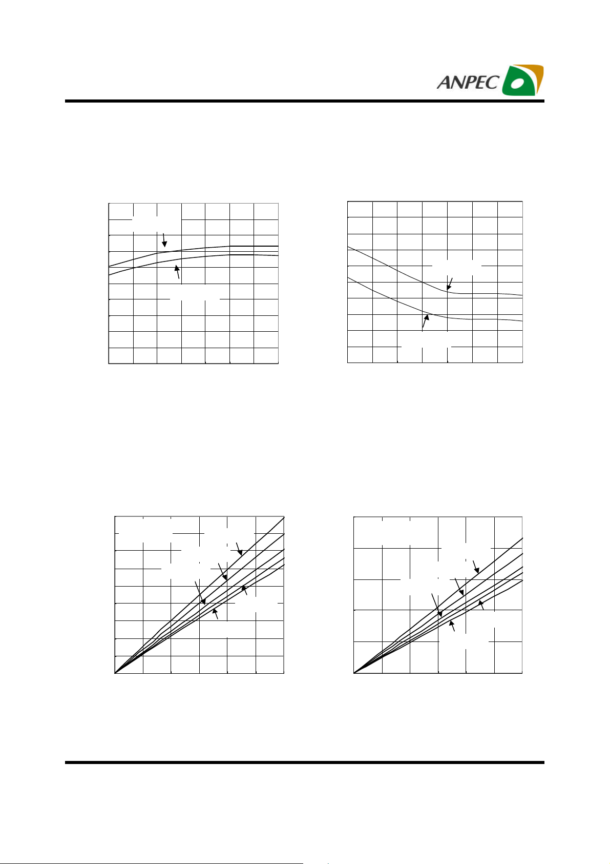
APL5913
Typical Operating Characteristics
VCNTL Supply Current vs.
Junction Temperature
1.0
0.9
0.8
0.7
0.6
0.5
0.4
0.3
0.2
0.1
VCNTL Supply Current, ICNTL (mA)
0.0
-50 -25 0 25 50 75 100 125
V
=5V
CNTL
V
=3.3V
CNTL
Junction Temperature (°C)
Current-limit vs.
Junction Temperature
5.5
5.4
5.3
5.2
5.1
5
4.9
4.8
Current-limit, ILIM (A)
4.7
4.6
4.5
-50 -25 0 25 50 75 100 125
V
CNTL
=3.3V
V
=5V
CNTL
Junction Temperature (°C)
Dropout Voltage vs. Output Current
450
V
=3.3V
CNTL
V
OUT
=1.2V
TJ=125°C
TJ=75°C
TJ=25°C
TJ=-25°C
0
0.0 0.5 1.0 1.5 2.0 2.5 3.0
400
350
300
250
200
150
Dropout Voltage (mV)
100
50
Copyright ANPEC Electronics C orp.
Rev. A.7 - Apr., 2008
TJ=0°C
Dropout Voltage vs. Output Current
250
V
=5V
CNTL
V
=1.2V
OUT
200
TJ=125°C
TJ=75°C
150
100
50
Dropout Voltage (mV)
0
0.0 0.5 1.0 1.5 2.0 2.5 3.0
TJ=25°C
TJ=-25°C
Output Current, lOUT(A)Output Current, lOUT(A)
www.anpec.com.tw6
TJ=0°C
 Loading...