


APL5912
0.8V Reference Ultra Low Dropout (0.2V@5A) Linear Regulator
Features
• Ultra Low Dropout
- 0.2V (typical) at 5A Output Current
• Low ESR Output Capacitor (Multi-layer Chip
Capacitors (MLCC)) Applicable
• 0.8V Reference Voltage
• High Output Accuracy
- ±1.5% over Line, Load and Temperature
• Fast Transient Response
• Adjustable Output Voltage by External
Resistors
• Power-On-Reset Monitoring on Both VCNTL and
VIN Pins
• Internal Soft-Start
• Current-Limit Protection
• Under-Voltage Protection
• Thermal Shutdown with Hysteresis
• Power-OK Output with a Delay Time
General Description
The APL5912 is a 5A ultra low dropout linear regulator.
This product is specifically designed to provide well supply voltage for front-side-bus termination on motherboard
and NB applications. The IC needs two supply voltages, a
control voltage for the circuitry and a main supply volatege
for power conversion, to reduc e power dissipation and
provide extremely low dropout.
The APL5912 integrates many functions. A Power-OnReset (POR) circuit monitors both supply voltages to prevent wrong operations. A thermal s hutdown and current
limit functions protect the device against thermal and current over-loads. A POK indicates the output status with
time delay which is set internally. It can control other converter for power sequence. The APL5912 is enabled by
other power system. Pulling and holding the EN pin below 0.3V shuts off the output.
The APL5912 is available in SOP-8P package which features small size as SOP-8 and an Exposed Pad to reduce
the junction-to-case resistanc e, being applicable in
2~2.5W applications.
• Shutdown for Standby or Suspend Mode
• Simple SOP-8P Package with Exposed Pad
• Lead Free and Green Devices Available
(RoHS Compliant)
Applications
• Front Side Bus VTT (1.2V/5A)
• Note Book PC Applications
• Motherboard Applications
Copyright ANPEC Electronics Corp.
Rev. A.9 - Apr., 2008
Pin Configuration
1
GND
2
FB
VOUT
VOUT
SOP-8P (Top View)
(connected to VIN plane for better heat
dissipation)
= Exposed Pad
VIN
3
4
8
7
6
5
EN
POK
VCNTL
VIN
www.anpec.com.tw1
APL5912
o
Ordering and Marking Information
APL5912
Assembly Material
Handling Code
Temperature Range
Package Code
Package Code
KA : SOP-8P
Operating Ambient Temperature Range
C : 0 to 70 C
Handing Code
TR : Tape & Reel
Assembly Material
L : Lead Free Device
G : Halogen and Lead Free Device
APL5912 KA :
APL5912
XXXXX
XXXXX - Date Code
Note: ANPEC lead-free products contain molding compounds/die attach materials and 100% matte tin plate termination finish; which
are fully compliant with RoHS. ANPEC lead-free products meet or exceed the lead-free requirements of IPC/JEDEC J-STD-020C for
MSL classification at lead-free peak reflow temperature. ANPEC defines “Green” to mean lead-free (RoHS compliant) and halogen
free (Br or Cl does not exceed 900ppm by weight in homogeneous material and total of Br and Cl does not exceed 1500ppm by
weight).
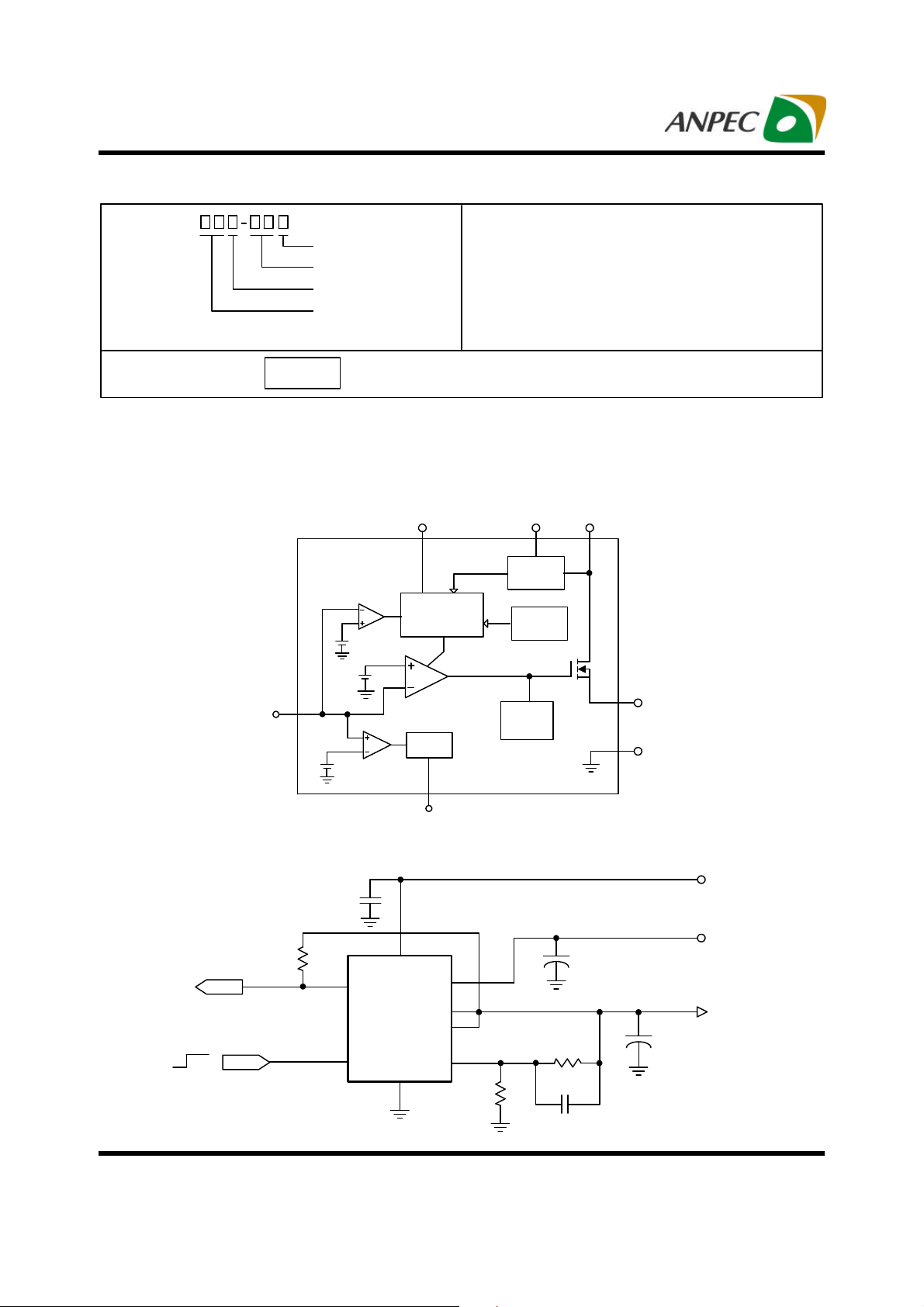
Block Diagram
0.4V
UV
EN
Soft-Start
and
Control Logic
Power-
On-Reset
Thermal
Limit
VINVCNTL
VREF
0.8V
FB
POK
90%
VREF
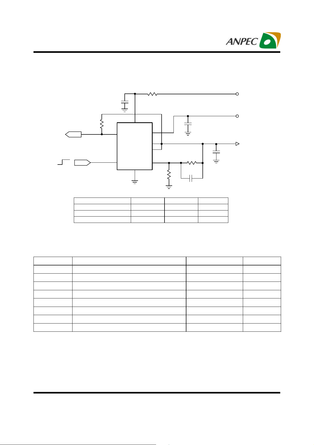
Typical Application Circuit
1. Using an Output Capacitor with ESR≥18mΩ
C
CNTL
1µF
R3
1k
POK
EN
Enable
7
POK
APL5912
8
EN
EAMP
6
VCNTL
GND
1
Delay
POK
VIN
VOUT
VOUT
FB
Current
Limit
VOUT
GND
VCNTL
+5V
VIN
OUT
+1.5V
VOUT
+1.2V / 5A
C
IN
5
3
4
2
R2
2k
100µF
R1
1k
C1
(in the range of 12 ~ 48nF)
33nF
C
220µF
Copyright ANPEC Electronics C orp.
www.anpec.com.tw2
Rev. A.9 - Apr., 2008
APL5912
Typical Application Circuit (Cont.)
2. Using an MLCC as the Output Capacitor
R4
10 (in the range of 5.1~15Ω)
6
5
VIN
FB
3
4
2
VOUT
VOUT
1
Enable
POK
EN
R3
1k
C
1µF
CNTL
7
8
VCNTL
POK
APL5912
EN
GND
R2
78k
R1
39k
C1
30pF
C
IN
22µF
C
OUT
22µF
V
CNTL
+5V
V
IN
+1.5V
V
OUT
+1.2V / 5A
V
OUT
(V)
R1 (kΩ) R2 (kΩ)
C1 (pF)
1.05 43 137.6 27
1.5 27 30.86 36
1.8 15 12 68
Absolute Maximum Ratings
Symbol Parameter Rating Unit
V
VCNTL Supply Voltage (VCNTL to GND) -0.3 ~ 7 V
CNTL
VIN VIN Supply Voltage (VIN to GND) -0.3 ~ 3.3 V
V
EN and FB to GND -0.3 ~ V
I/O
V
POK to GND -0.3 ~ 7 V
POK
PD Power Dissipation 3 W
TJ Junction Temperature 150
T
Storage Temperature -65 ~ 150
STG
T
Maximum Lead Soldering Temperature, 10 Seconds 260
SDR
+0.3 V
CNTL
o
C
o
C
o
C
Copyright ANPEC Electronics C orp.
Rev. A.9 - Apr., 2008
www.anpec.com.tw3
APL5912
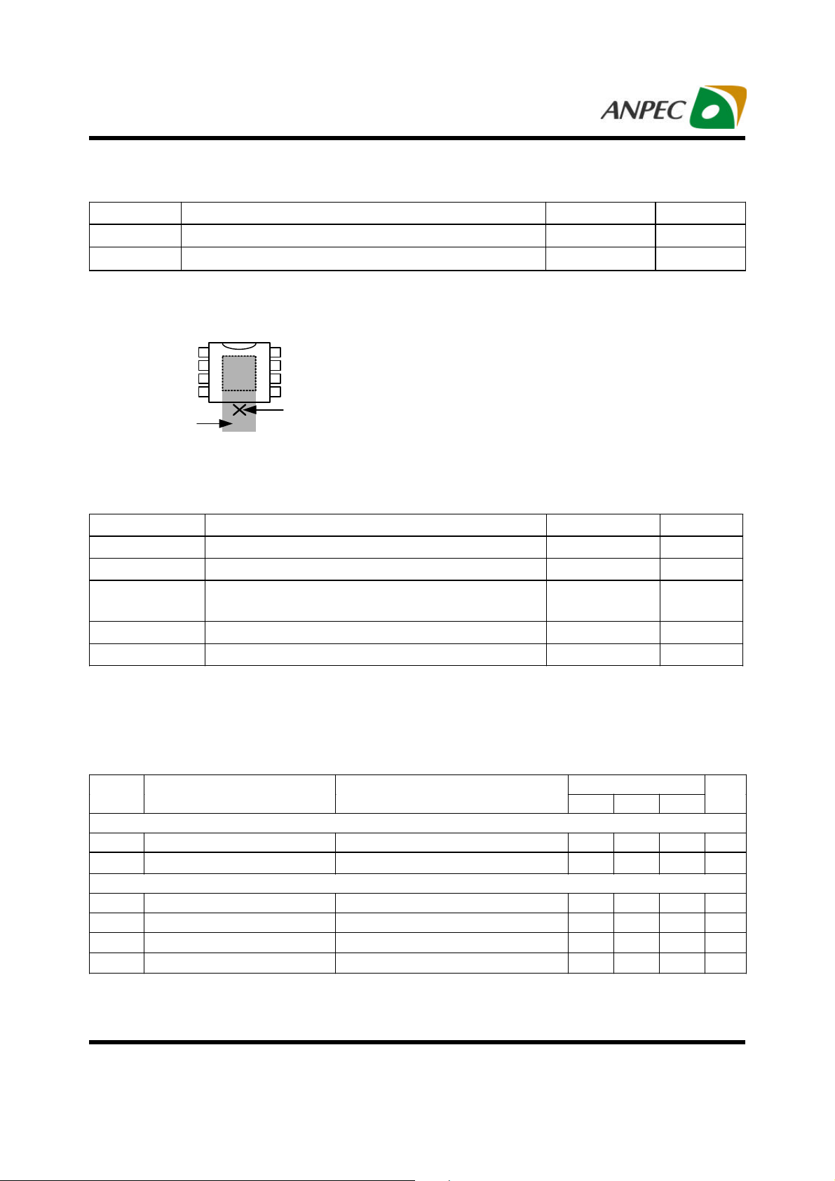
Thermal Characteristics
Symbol Parameter Value Unit
Junction-to-Ambient Thermal Resistance in Free Air
Junction-to-Case Thermal Resistance
(Note 2)
17
is measured with the component mounted on a high effective thermal conductivity test board in free air. The exposed pad
Note 1 : θ
θ
JA
θJC
JA
of SOP-8P is soldered directly on the PCB.
Note 2 : The “Thermal Pad Temperature” is measured on the PCB copper area connected to the thermal pad of package.
(Note 1)
40
o
C/W
o
C/W
1
2
VIN
3
4
8
7
6
5
Measured Point
PCB Copper
Recommended Operating Conditions
Symbol Parameter Range Unit
V
VCNTL Supply Voltage 3.1 ~ 6 V
CNTL
VIN VIN Supply Voltage 1.1 ~ 3.3 V
OUT
I
VOUT Output Current 0 ~ 6 A
OUT
V
V
CNTL
CNTL
=3.3±5%
=5.0±5%
V
Output Voltage
0.8 ~ 1.2
0.8 ~ VIN-0.2
TJ Junction Temperature -25 ~ 125
Electrical Characteristics
Refer to “Typical Applic ation Circuits”. These specifications apply over, V
70°C, unless otherwise specified. Typical values refer to TA =25°C.
=5V, VIN=1.5V, V
CNTL
OUT
V
o
C
= 1.2V and TA=0 to
Symbol
Parameter Test Conditions
APL5912
Min Typ Max
Unit
SUPPLY CURRENT
I
VCNTL Supply Current EN = VCNTL, VFB is well regulated. 0.4 1 2 mA
CNTL
ISD VCNTL Shutdown Current EN = GND 180 380
µ
A
POWER-ON-RESET
VCNTL POR Threshold V
Rising 2.7 2.9 3.1 V
CNTL
VCNTL POR Hysteresis 0.4 V
VIN POR Threshold VIN Rising 0.8 0.9 1.0 V
VIN POR Hysteresis 0.5 V
Copyright ANPEC Electronics C orp.
Rev. A.9 - Apr., 2008
www.anpec.com.tw4
APL5912
Electrical Characteristics (Cont.)
Refer to “Typical Application Circuit”. These specifications apply over, V
= 5V, VIN = 1.5V, V
CNTL
= 1.2V and TA = 0 to
OUT
70°C, unless otherwise specified. Typical values refer to TA =25°C.
Symbol
Parameter Test Conditions
OUTPUT VOLTAGE
V
Reference Voltage FB =VOUT 0.8 V
REF
Output Voltage Accuracy I
Line Regulation V
Load Regulation I
=0A ~ 5A, TJ= -25 ~125oC -1.5 +1.5 %
OUT
=3.3 ~ 5.5V -0.13 0.13 %/V
CNTL
=0A ~ 5A 0.06 0.15 %
OUT
DROPOUT VOLTAGE
Dropout Voltage
I
OUT
OUT
= 5A, V
= 5A, V
=5V, TJ= 25oC 0.15 0.2 V
CNTL
=5V, TJ= -25~125oC 0.25 V
CNTL
I
PROTECTION
V
=5V, TJ= 25oC 7 8 9 A
CNTL
V
=5V, TJ= -25 ~ 125oC 6 A
I
Current Limit
LIM
CNTL
V
=3.3V, TJ= 25oC 6.8 7.8 8.8 A
CNTL
V
=3.3V, TJ= -25 ~ 125oC 6 A
CNTL
TSD Thermal Shutdown Temperature TJ Rising 150
Thermal Shutdown Hysteresis 50
Under-Voltage Threshold VFB Falling 0.4 V
ENABLE AND SOFT-START
EN Logic High Threshold Voltage VEN Rising 0.3 0.4 0.5 V
EN Hysteresis 30 mV
EN Pin Pull-Up Current EN=GND 10
TSS Soft-Start Interval 2 ms
POWER OK AND DELAY
POK Threshold Voltage for
POK
Power OK
POK Threshold Voltage for
Power Not OK
VFB Rising 90% 92% 94% V
VFB Falling 79% 81% 83% V
V
V
PNOK
POK Low Voltage POK sinks 5mA 0.25 0.4 V
T
POK Delay Time 1 3 10 ms
DELAY
APL5912
Min Typ Max
Unit
o
C
oC
µ
A
REF
REF
Copyright ANPEC Electronics C orp.
www.anpec.com.tw5
Rev. A.9 - Apr., 2008
APL5912
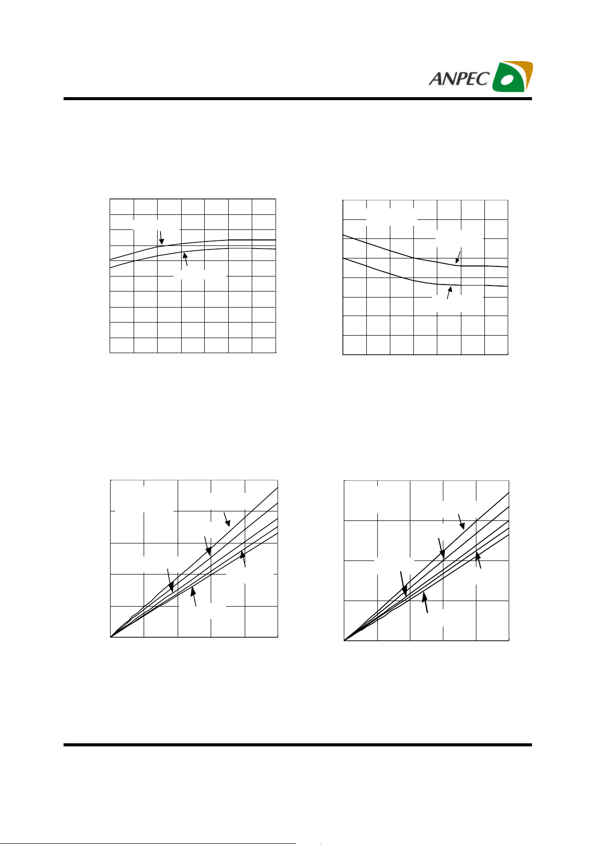
Typical Operating Characteristics
VCNTL Supply Current vs.
Junction Temperature
1.0
0.9
V
= 5V
(mA)
CNTL
0.8
0.7
CNTL
0.6
V
0.5
CNTL
= 3.3V
0.4
0.3
0.2
VCNTL Supply Current, I
0.1
0.0
-50 -25 0 25 50 75 100 125
Junction Temperature (°C)
Dropout Voltage vs. Output Current
Current-limit vs. Junction Temperature
8.6
V
=1.2V
8.4
8.2
8
(A)
LIM
7.8
7.6
7.4
Current-limit, I
7.2
7
-50 -25 0 25
OUT
V
CNTL
V
=3.3V
CNTL
75 100 125
50
Junction Temperature (°C)
Dropout Voltage vs. Output Current
=5V
250
V
=3.3V
200
V
CNTL
OUT
=1.2V
TJ=125 C
TJ=75 C
150
TJ=25 C
100
Dropout Voltage (mV)
50
TJ=-25 C
0
0 1 2 3 4 5
Output Current, l
OUT
Copyright ANPEC Electronics C orp.
Rev. A.9 - Apr., 2008
(A)
TJ=0 C
200
V
=5V
CNTL
V
=1.2V
OUT
TJ=125 C
150
TJ=75 C
100
Dropout Voltage (mV)
50
TJ=25 C
TJ=-25 C
0
0 1 2 3 4 5
Output Current, l
OUT
(A)
www.anpec.com.tw6
TJ=0 C

APL5912
Typical Operating Characteristics
Reference Voltage vs. Junction Temperature
0.808
0.806
0.804
(mV)
REF
0.802
0.800
0.798
0.796
Reference Voltage, V
0.794
0.792
-50 -25 0 25 50 75 100 125
Junction Temperature (°C)
POK Delay Time vs. Junction Temperature
4.5
4.3
4.1
3.9
3.7
3.5
3.3
3.1
POK Delay Time (ms)
2.9
2.7
2.5
-50 -25 0 25 50 75 100 125
V
=5V
CNTL
V
=3.3V
CNTL
Junction Temperature (°C)
VCNTL PSRR
0.00
V
= 4.5V~5.5V
CNTL
VIN = 1.5V
-10.00
V
= 1.2V
OUT
I
= 5A
OUT
CIN = 100µF
C
-20.00
-30.00
-40.00
-50.00
Ripple Rejection (dB)
-60.00
-70.00
Copyright ANPEC Electronics C orp.
Rev. A.9 - Apr., 2008
= 330µF(ESR=30mΩ)
OUT
100 1000 10000 100000 1000000
Frequency (Hz)
VIN PSRR
0
V
= 5V
CNTL
VIN = 1.5V(lower bound)
V
-10
-20
-30
-40
Amplitude (dB)
-50
-60
= 100mV
INPK-PK
CIN = 47µF
C
= 330µF(30m ohm)
OUT
I
= 5A
OUT
V
= 1.2V
OUT
100 1000 10000 100000 1000000
Frequency (Hz)
www.anpec.com.tw7

APL5912
Operating Waveforms
Test Circuit
R4
R8
8.2K
Shutdown
C8
470pF
Q3
7
6
5
VCC
OCSET
UGATE
PHASE
U2
APW7057
FB
LGATE
GND
3
C2
1µF
BOOT
1
2
8
4
2.2
D1
1N4148
C6
0.1µF
R7
2K
C3
1µF
Q1
APM2014N
Q2
APM2014N
R5
1.75k
C7
0.1µF
1. Load transient Response
1.1 Using an Output Capacitor with ESR≥18mΩ
- C
- I
= 220µF/6.3V (ESR = 30mΩ), CIN = 100µF/6.3V
OUT
= 10mA to 5A to 10mA, Rise time = Fall time = 1µs
OUT
R6
0
L2
3.3µH
L1
1µH
C4
470µF x2
1000µF x2
C5
Enable
C9
47µF
VIN
+1.5V
EN
CVCNTL
1µF
CIN
100µF
8
5
VCNTL
VIN
U1
APL5912
EN
GND
VCNTL
+5V
6
POK
VOUT
VOUT
1
+5V
FB
2
R2
2K
POK
R3
7
3
4
1K
VOUT
+1.2V/5A
COUT
220µF
R1
1K
C1
33nF
I
= 10mA ->5A I
OUT
11
VOUT
IOUT
22
Ch1 : V
Ch2 : I
, 50mV/Div
OUT
, 2A/Div
OUT
Time : 2µs/Div
Copyright ANPEC Electronics C orp.
Rev. A.9 - Apr., 2008
= 10mA -> 5A ->10mA I
OUT
R1=1kΩ, R2=2kΩ, C1=33nF
11
22
Ch1 : V
Ch2 : I
, 50mV/Div
OUT
, 2A/Div
OUT
Time : 20µs/Div
VOUT
IOUT
11
22
Ch1 : V
Ch2 : I
Time : 2µs/Div
= 5A ->10mA
OUT
, 50mV/Div
OUT
, 2A/Div
OUT
www.anpec.com.tw8
VOUT
IOUT

APL5912
Operating Waveforms (Cont.)
1.2 Using an MLCC as the Output Capacitor
- C
- I
11
= 22µF/6.3V (ESR = 3mΩ), CIN = 22µF/6.3V
OUT
= 10mA to 5A to 10mA, Rise time = Fall time = 1µs
OUT
I
= 10mA -> 5A I
OUT
= 10mA -> 5A ->10mA I
OUT
R1=39kΩ, R2=78kΩ,
R3=30nF
11
V
OUT
= 5A ->10mA
OUT
V
11
V
OUT
OUT
I
OUT
22
Ch1 : V
Ch2 : I
, 100mV/Div
OUT
, 2A/Div
OUT
Time : 2µs/Div
2. Power ON and Power OFF :
- V
- C
Ch1
Ch2
Ch3
= 1.5V, V
IN
= 220µF/6.3V (ESR = 30mΩ), CIN = 100µF/6.3V, RL = 1Ω
OUT
Power ON
CNTL
= 5V,V
V
V
V
V
POK
OUT
IN
OUT
CNTL
= 1.2V
22
Ch1 : V
Ch2 : I
Time : 20µs/Div
I
OUT
, 100mV/Div
OUT
, 2A/Div
OUT
Ch1
Ch1
Ch2
Ch2
Ch3
Ch3
22
Ch1 : V
Ch2 : I
Time : 2µs/Div
, 100mV/Div
OUT
, 2A/Div
OUT
Power OFF
Power OFF
V
VIN
VINVIN
IN
V
OUT
VOUT
VOUTVOUT
V
VCNTL
VCNTLVCNTL
CNTL
V
VPOK
VPOKVPOK
POK
I
OUT
Ch4
Ch1 : VIN, 1V/div
Ch2 : V
Ch3 : V
Ch4 : V
OUT
POK
CNTL
,1V/div
,1V/div
,2V/div
Time : 10ms/div
Copyright ANPEC Electronics C orp.
Rev. A.9 - Apr., 2008
Ch4
Ch4
Ch1 : VIN, 1V/div
Ch2 : V
Ch3 : V
Ch4 : V
OUT
POK
CNTL
, 1V/div
, 1V/div
, 2V/div
Time : 10ms/div
www.anpec.com.tw9

APL5912
Operating Waveforms (Cont.)
3. Shutdown and Enable :
- V
- C
Ch1
Ch1
= 1.5V, V
IN
= 220µF/6.3V (ESR = 30mΩ), CIN = 100µF/6.3V, RL = 1Ω
OUT
CNTL
= 5V, V
OUT
= 1.2V
Shutdown
Shutdown
V
VEN
VENVEN
EN
Ch1
Ch1
Enable
Enable
V
VEN
VENVEN
EN
Ch2
Ch2
Ch3
Ch3
Ch4
Ch4
Ch1 : VEN, 5V/div
Ch2 : V
Ch3 : I
Ch4 : V
OUT
OUT
POK
, 1V/div
, 1A/div
, 1V/div
Time : 1ms/div
4. POK Delay :
- V
- C
Ch1
Ch1
= 1.5V, V
IN
= 220µF/6.3V (ESR = 30mΩ), CIN = 100µF/6.3V, RL = 1Ω
OUT
V
IN
VIN
VINVIN
CNTL
= 5V, V
= 1.2V
OUT
POK Delay
POK Delay
V
VOUT
VOUTVOUT
OUT
I
IOUT
IOUTIOUT
OUT
V
VPOK
VPOKVPOK
POK
Ch2
Ch2
Ch3
Ch3
Ch4
Ch4
Ch1 : VEN, 5V/div
Ch2 : V
Ch3 : I
Ch4 : V
Time : 1ms/div
V
VOUT
VOUTVOUT
OUT
I
IOUT
IOUTIOUT
OUT
V
VPOK
VPOKVPOK
OUT
, 1A/div
OUT
POK
POK
, 1V/div
, 1V/div
V
VOUT
VOUTVOUT
OUT
Ch2
Ch2
V
VPOK
VPOKVPOK
Ch3
Ch3
POK
Ch1 : VIN, 5V/div
Ch2 : V
Ch3 : V
, 1V/div
OUT
, 1V/div
POK
Time : 1ms/div
Copyright ANPEC Electronics C orp.
Rev. A.9 - Apr., 2008
www.anpec.com.tw10

APL5912
Functional Pin Description
GND (Pin 1)
Ground pin of the circuitry. All voltage levels are measured
with respect to this pin.
FB (Pin 2)
Connecting this pin to an external resistor divider receives the feedback voltage of the regulator. The output
voltage set by the resistor divider is determined by :
where R1 is c onnected from VOUT to FB with Kelvin
sensing and R2 is connected from FB to GND. A bypass capacitor may be c onnected with R1 in parallel to
improve load transient response.
VOUT (Pin 3, 4)
Output of the regulator. Please c onnect Pin 3 and 4 together using wide tracks . It is necessary to connect a
output capacitor with this pin for closed-loop compensation and improve transient res ponses.
VIN (Pin 5) and Exposed Pad
R1
+⋅=
10.8 VOUT
R2
(V)
VCNTL (Pin 6)
Power input pin of the control circuitry. Connecting this
pin to a +5V (recommended) supply voltage provides the
bias for the control circuitry. The voltage at this pin is
monitored for Power-On-Reset purpose.
POK (Pin 7)
Power-OK signal output pin. This pin is an open-drain
output used to indicate status of output voltage by sensing FB voltage. This pin is pulled low when the rising FB
voltage is not above the V
voltage is below the V
is not OK.
EN (Pin 8)
Enable c ontrol pin. Pulling and holding this pin below
0.3V shuts down the output. When re-enabled, the IC
undergoes a new soft-start cyc le. When leave this pin
open, an internal current source 10µA pulls this pin up to
VCNTL voltage, enabling the regulator.
PNOK
threshold or the falling FB
POK
threshold, indicating the output
Main supply input pins for power convers ions. The Exposed Pad provides a very low impedance input path for
the main supply voltage. Please tie the Exposed Pad and
VIN Pin (Pin 8) together to reduce the dropout voltage. The
voltage at this pins is monitored for Power-On-Reset
purpose.
Function Description
Power-On-Reset
A Power-On-Reset (POR) circuit monitors both input voltages at VCNTL and VIN pins to prevent wrong logic
controls. The POR function initiates a soft-start proc ess
after the two supply voltages exceed their rising POR
thres hold voltages during powering on. The POR function also pulls low the POK pin regardless the output
voltage when the VCNTL voltage falls below its falling
POR threshold.
Internal Soft-Start
An internal s oft-start function controls rising rate of the
output voltage to limit the current surge at start-up. The
typical soft-start interval is about 2ms.
Output Voltage Regulation
An error amplifier works with a tem perature-compensated 0.
8V reference and an output NMOS regulates output to the
preset voltage. The error amplifier is designed with high
bandwidth and DC gain provides very fast transient re-
Copyright ANPEC Electronics C orp.
Rev. A.9 - Apr., 2008
www.anpec.com.tw11

APL5912
Function Description (Cont.)
Output Voltage Regulation (Cont.) For normal operation, devic e power dissipation should
sponse and less load regulation. It c ompares the refer-
ence with the feedback voltage and amplifies the difference to drive the output NMOS which provides load current from VIN to VOUT.
Current-Limit
The APL5912 monitors the current via the output NMOS
and limits the maximum current to prevent load and
APL5912 from damages during overload or short-circ uit
conditions.
Under-Voltage Protection (UVP)
The APL5912 monitors the voltage on FB pin after softstart proc ess is finished. Therefore, the UVP is disable
during soft-start. When the voltage on FB pin falls below
the under-voltage threshold, the UVP circuit shuts off the
output immediately. After a while, the APL5912 starts a
new soft-start to regulate output.
Thermal Shutdown
A thermal shutdown circuit limits the junction temperature of
APL5912. When the junction temperature exceeds
+150°C, a thermal sensor turns off the output NMOS,
allowing the device to cool down. The regulator regulates
the output again through initiation of a new soft-start
cycle after the junction temperature cools by 50oC, resulting in a pulsed output during continuous thermal overload conditions. The thermal shutdown is designed with
a 50oC hysteresis to lower the average junction temperature during continuous thermal overload conditions, extending lifetime of the device.
be externally limited s o that junction temperatures will
not exceed +125°C.
Enable Control
The APL5912 has a dedicated enable pin (EN). A logic
low signal (VEN< 0.3V) applied to this pin shuts down the
output. Following a s hutdown, a logic high signal re-enables the output through initiation of a new softstart cycle.
Left open, this pin is pulled up by an internal current source
(10µA typical) to enable operation. It’s not necessary to use
an external transistor to save cos t.
Power-OK and Delay
The APL5912 indicates the status of the output voltage by
monitoring the feedback voltage (VFB) on FB pin. As the
VFB rises and reaches the rising Power-OK threshold
(V
), an internal delay function starts to perform a delay
POK
time. At the end of the delay time, the IC turns off the
internal NMOS of the POK to indicate the output is OK. As
the VFB falls and reaches the falling Power-OK threshold
(V
), the IC immediately turns on the NMOS of the POK to
PNO K
indicate the output is not OK without a delay time.
Application Information
Power Sequencing
The power s equencing of VIN and VCNTL is not necessary to be concerned. However, do not apply a voltage to
VOUT for a long time when the main voltage applied at
VIN is not present. The reason is the internal parasitic
diode from VOUT to VIN conducts and dissipates power
without protections due to the forward-voltage.
Copyright ANPEC Electronics C orp.
Rev. A.9 - Apr., 2008
Output Capacitor
The APL5912 requires a proper output capacitor to maintain stability and improv e transient response over temperature and current. The output capacitor selection is to
select proper ESR (equivalent s eries resistance) and
capacitance of the output capacitor for good stability and
load transient response.
www.anpec.com.tw12

APL5912
Application Information (Cont.)
Output Capacitor (Cont.)
The APL5912 is designed with a programmable feedback
compensation adjusted by an external feedback network for
the use of wide ranges of ESR and capacitance in all
applications. Ultra-low-ESR capacitors (such as ceramic
chip capacitors) and low-ESR bulk capacitors (such as
solid tantalum, POSCap, and Aluminum electrolytic
capacitors) can all be used as an output capacitor. The
value of the output capacitors c an be increased without
limit.
During load transients, the output capacitors, depending on
the stepping amplitude and slew rate of load current, are
used to reduce the s lew rate of the current seen by the
APL5912 and help the device to minimize the variations
of output voltage for good transient response. For the applications with large stepping load current, the low-ESR
bulk capacitors are normally recommended.
Decoupling ceramic capacitors must be placed at the load
and ground pins as close as possible and the impedance of the layout must be minimized.
Input Capacitor
The APL5912 requires proper input capacitors to supply
current surge during stepping load transients to prevent
the input rail from dropping . Because the parasitic inductor from the voltage sources or other bulk capacitors to the
VIN pin limit the s lew rate of the surge currents, more
parasitic inductance needs more input capacitance.
Ultra-low-ESR capacitors (such as ceramic chip
capacitors) and low-ESR bulk capacitors (such as solid
tantalum, POSCap, and Aluminum electrolytic capacitors)
can all be used as an input capacitor of VIN. For most of
applications, the recommended input capacitance of VIN
is 10µF at least. If the drop of the input voltage is not
cared, the input capacitance can be less than 10µF. More
capacitance reduces the variations of the input voltage of
VIN pin.
Feedback Network
Figure 1 shows the feedback network among VOUT, GND,
and FB pins. It works with the internal error amplifier to
provide proper frequency response for the linear regulator.
The ESR is the equivalent series resistance of the output
capacitor. The C
capacitor. The V
is ideal capacitance in the output
OUT
is the setting of the output voltage.
OUT
VOUT
VOUT
APL5912
ESR
COUT
VERR
EAMP
VREF
FB
VFB
Figure 1
R1
R2
C1
The feedback network selection, depending on the values of the ESR and C
, has been classified into three
OUT
conditions :
• Condition 1 : Large ESR ( ≥18mΩ )
- Select the R1 in the range of 400Ω ~ 2.4kΩ
- Calculate the R2 as the following:
0.8(V)
)R1(k)R2(k
⋅Ω=Ω
OUT
0.8(V)-(V)V
(1) ..........
- Calculate the C1 as the following:
10
(V)V
⋅
)R1(k
Ω
40C1(nF)
(V)V
OUTOUT
⋅≤≤
Ω
(2) ......
)R1(k
• Condition 2 : Middle ESR
- Calculate the R1 as the following:
1500
)R1(k OUT +⋅−
=Ω
)ESR(m
Ω
(3) ......... 30(V)V37.5
Select a proper R1(selected) to be a little larger than
the calculated R1.
- Calculate the C1 as the following:
F)(C
OUT
[ ]
Where R1=R1
Select a proper C1
(selected)
50)ESR(mC1(pF)
(selected)
µ
⋅+Ω=
)R1(k
Ω
(4) ...................
to be a little smaller than the
calculated C1.
- The C1 calculated from equation (4) must meet
the following equation :
50
)ESR(m
Ω
⋅
1
+⋅
15.1C1(pF)
+⋅≥
OUT
Ω
(V)V37.5
(5) ..
)R1(k
Copyright ANPEC Electronics C orp.
Rev. A.9 - Apr., 2008
www.anpec.com.tw13

APL5912
Application Information (Cont.)
Feedback Network (Cont.)
Where R1=R1(calculated) from equation (3)
If the C1(calculated) can not meet the equation
(5), please use the Condition 3.
- Use equation (2) to calc ulate the R2.
• Condition 3: Low ESR (eg. Ceramic Capacitors)
- Calculate the R1 as the following:
Select a proper R1(selected) to be a little larger than
the calculated R1. The minimum selected R1 is
equal to 1kΩ when the calculated R1 is smaller
than 1k or negative.
- Calculate the C1 as the following :
(V)V37.5
OUT
⋅
)R1(k
Ω
Where R1=R1
(selected)
OUT
1F)(C8.5))ESR(m(0.17C1(pF)
+⋅µ⋅+Ω⋅=
Select a proper C1(selected) to be a little smaller
than the calculated C1.
- The C1 calculated from equation (7) must meet
the following equation :
0.033C1(pF) OUT
⋅
+≥
OUT
Ω
(V)V1.25
)R1(k
µ⋅Ω⋅
Where R1=R1(calculated) from equation (6)
PCB Layout Consideration (See Figure 2)
1. Please solder the Exposed Pad and VIN together on
the PCB. The main current flow is through the exposed
pad.
2. Please place the input capacitors for VIN and VCNTL
pins near pins as clos e as possible.
3. Ceramic decoupling capacitors for load must be placed
near the load as close as possible.
4. To place APL5912 and output capacitors near the load
is good for performance.
(6) .. (V)V37.5F)(C294))ESR(m(5.9)R1(k OUTOUT ⋅−µ⋅+Ω⋅=Ω
5. The negative pins of the input and output capacitors
and the GND pin of the APL5912 are connected to the
ground plane of the load.
6. Please connect PIN 3 and 4 together by a wide track or
plane on the Top layer.
7. Large current paths must have wide tracks.
8. See the Typical Application
- Connect the one pin of the R2 to the GND of APL5912.
(7) ..
V
CNTL
C
CNTL
VCNTL
APL5912
(8) .. F)(C)ESR(m
VIN
VOUT
VOUT
C1
FB
GND
R2
R1
C
IN
C
OUT
V
IN
V
OUT
Load
If the C1(calculated) can not meet the equation
(8), please use the Condition 2.
- Use equation (2) to calculate the R2.
The reason to have three conditions desc ribed above is
to optimize the load transient respons es for all kinds of
the output capacitor. For stability only, the Condition 2, regardless of equation (5), is enough for all kinds of output
capacitor.
Copyright ANPEC Electronics C orp.
Rev. A.9 - Apr., 2008
Figure 2
- Connect the one pin of R1 to the Pin 3 of APL5912
- Connect the one pin of C1 to the Pin 3 of APL5912
www.anpec.com.tw14

APL5912
Application Information (Cont.)
Thermal Consideration
See Figure 3. The SOP-8P is a cost-effective package featuring a small size like a standard SOP-8 and a bottom
exposed pad to minimize the thermal resis tance of the
package, being applicable to high current applications.
The exposed pad must be soldered to the top VIN plane.
The copper of the VIN plane on the Top layer conducts heat
into the PCB and air. Please enlarge the area to reduce the
case-to-ambient resistance (θCA).
102 mil
1
2
3
4
SOP-8P
Exposed
Die
Ambient
Air
118 mil
Top
VOUT
plane
Figure 3
Recommended Minimum Footprint
8 7 6 5
0.138
0.212
Pad
0.024
8
7
6
5
PCB
Top
VIN
plane
0.072
0.118
1 2 3 4
0.050
Unit : Inch
Copyright ANPEC Electronics C orp.
Rev. A.9 - Apr., 2008
www.anpec.com.tw15

APL5912
Pack age Information
SOP-8P
D
D1
SEE VIEW
A
THERMAL
PAD
e
S
Y
M
B
O
L
A
A1
A2
b
c
D
D1
E
E1
E2
e
h
0
E
E1
E2
h X 45
cb
A
A1 A2
SOP-8P
MILLIMETERS
MIN.
0.00
1.25
0.31
0.17
4.80 5.00
2.25
5.80 6.20
3.80 4.00
2.00
1.27 BSC
0.25
0.40L
o
0
Note : 1. Follow JEDEC MS-012 BA.
2. Dimension "D" does not include mold flash, protrusions
or gate burrs. Mold flash, protrusion or gate burrs shall not
exceed 6 mil per side .
3. Dimension "E" does not include inter-lead flash or protrusions.
Inter-lead flash and protrusions shall not exceed 10 mil per side.
MAX.
1.60
0.15
0.51
0.25
3.50
3.00
0.50
1.27
o
8
VIEW A
MIN.
0.000
0.049
0.012
0.007
0.098
0.079
0.010
0.016
0
L
INCHES
0.050 BSC
o
0.25
GAUGE PLANE
SEATING PLANE
0
MAX.
0.063
0.006
0.020
0.010
0.1970.189
0.138
0.2440.228
0.1570.150
0.118
0.020
0.050
o
8
Copyright ANPEC Electronics C orp.
Rev. A.9 - Apr., 2008
www.anpec.com.tw16

APL5912
Carrier Tape & R eel Dimensions
OD0
B0
P0
P2
P1
A
E1
F
W
Application
SOP-8(P)
K0
SECTION A-A
B
HT1A
A0
SECTION B-B
OD1
B
T
A
d
A H T1 C d D W E1 F
330.0±
2.00
50 MIN.
12.4+2.00
-0.00
13.0+0.50
-0.20
1.5 MIN. 20.2 MIN.
12.0±0.30 1.75±0.10 5.5±0.05
P0 P1 P2 D0 D1 T A0 B0 K0
4.0±0.10 8.0±0.10 2.0±0.05
1.5+0.10
-0.00
1.5 MIN.
0.6+0.00
-0.40
6.40±0.20 5.20±0.20 2.10±0.20
(mm)
Devices Per Unit
Package Type Unit Quantity
SOP- 8P
Copyright ANPEC Electronics C orp.
Rev. A.9 - Apr., 2008
Tape & Reel 2500
www.anpec.com.tw17

APL5912
Reflow Condition (IR/Convection or VPR Reflow)
T
P
Ramp-up
T
L
Tsmax
Tsmin
Temperature
ts
Preheat
25
°
t 25 C to Peak
tp
t
Ramp-down
Critical Zone
TL to T
P
L
Time
Reliability Test Program
Test item Method Description
SOLDERABILITY MIL-STD-883D-2003
HOLT MIL-STD-883D-1005.7
PCT JESD-22-B, A102
TST MIL-STD-883D-1011.9
ESD MIL-STD-883D-3015.7 VHBM > 2KV, VMM > 200V
Latch-Up JESD 78 10ms, 1tr > 100mA
Classification Reflow Profiles
245°C, 5 sec
1000 Hrs Bias @125°C
168 Hrs, 100%RH, 121°C
-65°C~150°C, 200 Cycles
Profile Feature Sn-Pb Eutectic Assembly Pb-Free Assembly
Average ramp-up rate
(TL to TP)
Preheat
- Temperature Min (Tsmin)
- Temperature Max (Tsmax)
- Time (min to max) (ts)
Time maintained above:
- Temperature (TL)
- Time (tL)
Peak/Classification Temperature (Tp)
Time within 5°C of actual
Peak Temperature (tp)
Ramp-down Rate
Time 25°C to Peak Temperature
Note: All temperatures refer to topside of the package. Measured on the body surface.
Copyright ANPEC Electronics C orp.
Rev. A.9 - Apr., 2008
3°C/second max. 3°C/second max.
100°C
150°C
60-120 seconds
183°C
60-150 seconds
See table 1 See table 2
10-30 seconds 20-40 seconds
6°C/second max. 6°C/second max.
6 minutes max. 8 minutes max.
60-180 seconds
60-150 seconds
150°C
200°C
217°C
www.anpec.com.tw18

APL5912
Classification Reflow Profiles (Cont.)
Table 1. SnPb Eutectic Process – Package Peak Reflow Temperatures
Package Thickness Volume mm
<350
<2.5 mm
≥2.5 mm 225 +0/-5°C 225 +0/-5°C
240 +0/-5°C 225 +0/-5°C
3
Volume mm
≥
350
3
Table 2. Pb-free Process – Package Classification Reflow Temperatures
Package Thickness Volume mm3
<350
<1.6 mm
1.6 mm – 2.5 mm
≥2.5 mm 250 +0°C* 245 +0°C* 245 +0°C*
*Tolerance: The device manufacturer/supplier shall assure process compatibility up to and including the
stated classification temperature (this means Peak reflow temperature +0°C. For example 260°C+0°C)
at the rated MSL level.
260 +0°C* 260 +0°C* 260 +0°C*
260 +0°C* 250 +0°C* 245 +0°C*
Volume mm3
350-2000
Volume mm3
>2000
Customer Service
Anpec Electronics Corp.
Head Office :
No.6, Dusing 1st Road, SBIP,
Hsin-Chu, Taiwan
Tel : 886-3-5642000
Fax : 886-3-5642050
Taipei Branch :
2F, No. 11, Lane 218, Sec 2 Jhongsing Rd.,
Sindian City, Taipei County 23146, Taiwan
Tel : 886-2-2910-3838
Fax : 886-2-2917-3838
Copyright ANPEC Electronics C orp.
Rev. A.9 - Apr., 2008
www.anpec.com.tw19

 Loading...