

APL5158
150mA CMOS Low Dropout Regulator With Power OK
Features General Description
••
• Ultra low ground current : 60µA
••
••
• Low Dropout Voltage Regulator, 1.5V
••
••
• 150mA Load Current Capability
••
••
• Output Voltage Accuracy : ±2% Over Temp.
••
••
• Input Voltage Range of 2.7V to 6.0V
••
••
• Power Good (POK) Function
••
••
• Current Limit Protection
••
••
• Thermal Shutdown Protection
••
••
• Fast Transient Response
••
••
• Stability with low-ESR capacitors
••
••
• TTL Logic controlled enable input
••
••
• SOT-23-5 Package
••
Applications
• Processor power up sequencing
• Laptop,notebook, and palmtop computers
The APL5158 is a precise CMOS LDO with power ok
function. The APL5158 offers 2% output accuracy
over temp, and an ultra low ground current 60µA.
The power good function monitors the output voltage
and indicates when an error occurs in the system
(active low).In the event of an output fault such as
over current, thermal shutdown, the power ok output
is pulled low. The APL5158 also works with low-ESR
output capacitors, reducing the amount of board space
for power applications, critical in hand-held wireless
devices. Key features include current-limit, thermal
shutdown, fast transient response. A compact pack-
age SOT-23-5 is available for space saving purpose.
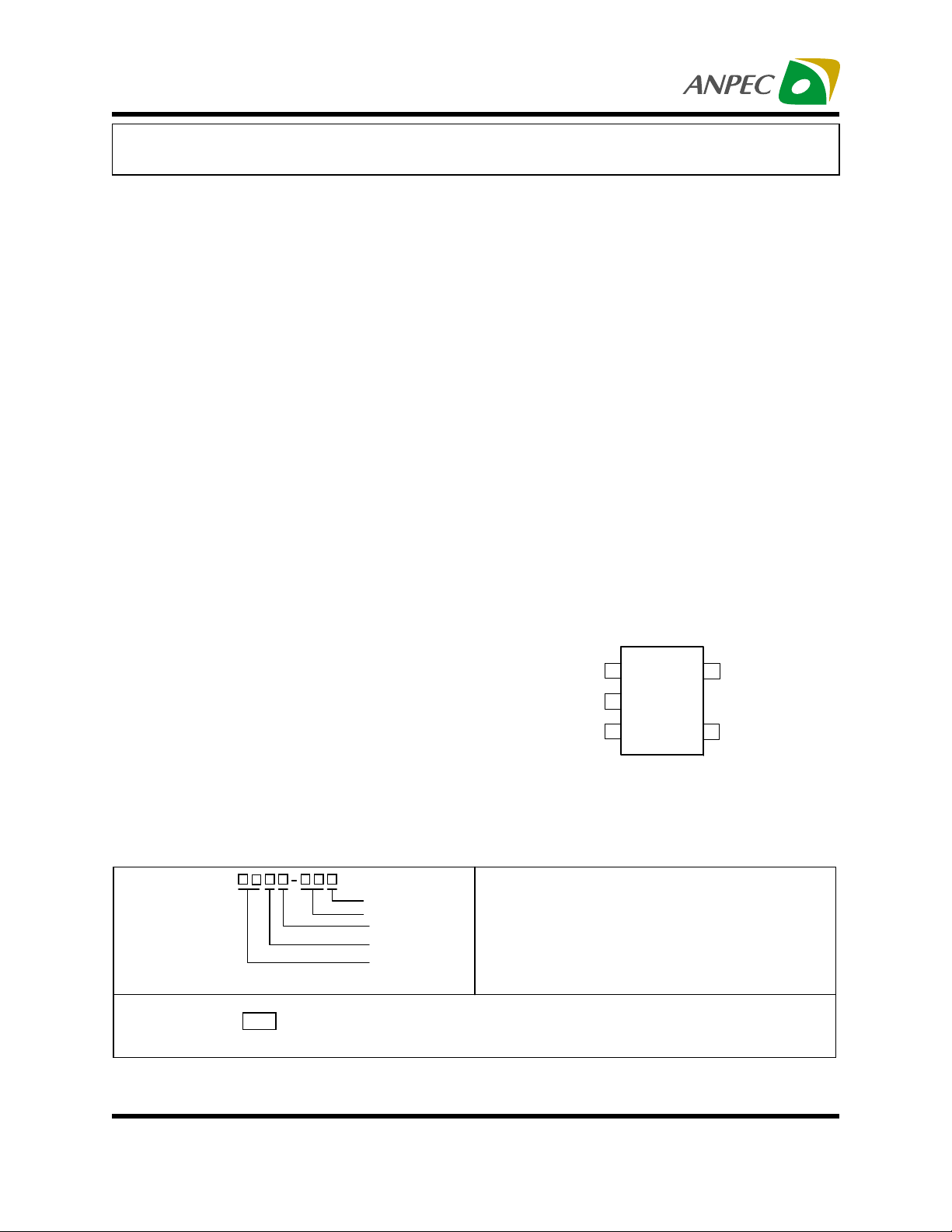
Pin Configuration
V
GND
EN
IN
1
2
3
5
4
OUT
V
POK
• Wireless LAN
SOT-23-5
Ordering and Marking Information
APL5158 -
Lead Free Code
Hand ling Code
Tem p. Ran ge
Package Code
Voltage C ode
185X
ANPEC reserves the right to make changes to improve reliability or manufacturability without notice, and advise
customers to obtain the latest version of relevant information to verify before placing orders.
Copyright ANPEC Electronics Corp.
Rev. A.4 - Aug., 2003
Package Code
B : S O T -2 3-5
Tem p. Ran ge
C : 0 to 7 0 C
Hand ling Code
TR : Tape & Reel
Voltage C ode :
1 2 : 1.2V
Lead Free Code
L : Le a d F re e D ev ice
B lan k : O rg ina l D ev ice
5 - 1 .2V
X - D ate C o de
°
www.anpec.com.tw1
APL5158
Pin Description
PIN
No. Name
I/O Description
1 VIN I Input supply voltage.
2 GND Ground pin for signal ground and power ground.
3 EN I Enable/shutdown input (active high). Do not leave open.
4 POK O Power OK indicator.
5 V
OUT
O Regulator output voltage.
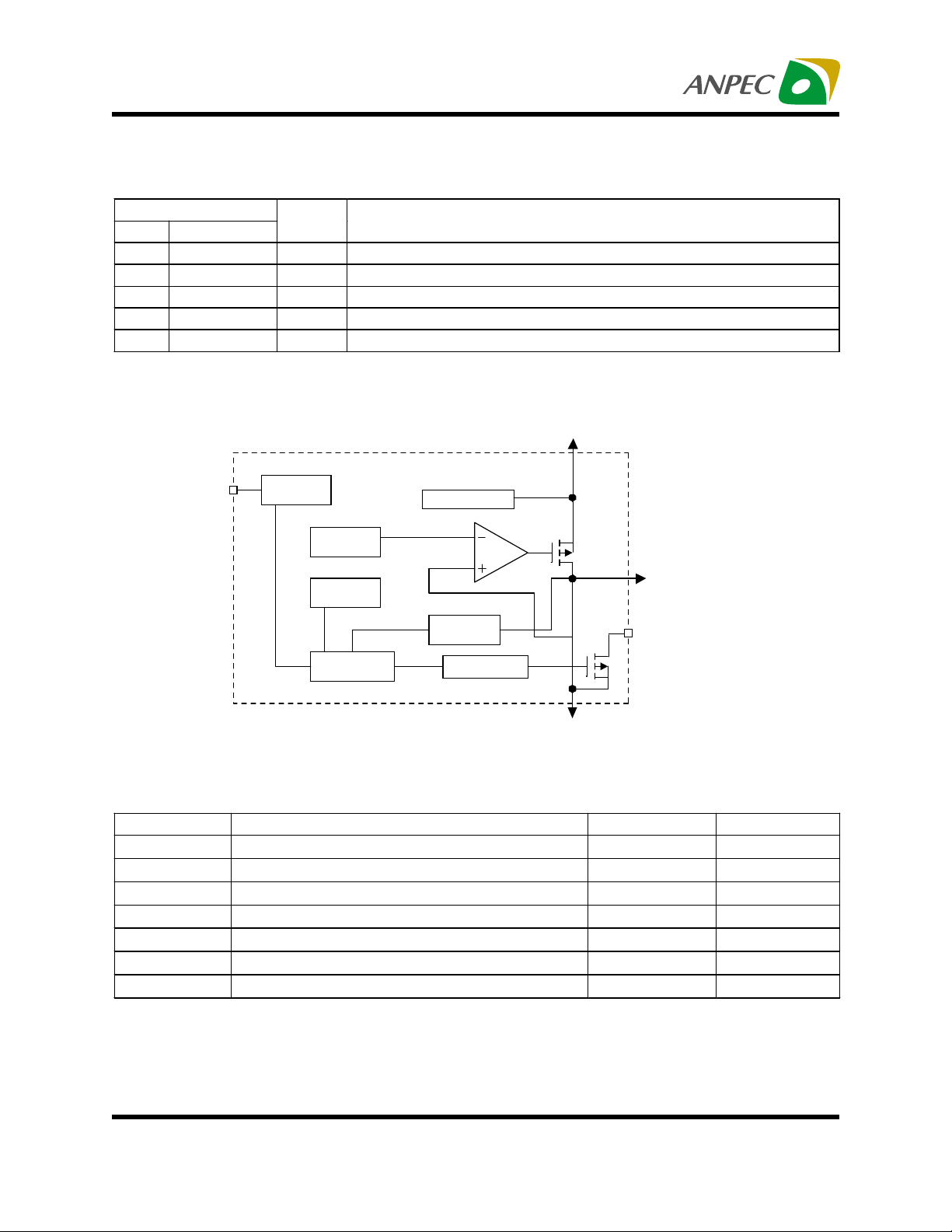
Block Diagram
V
IN
EN
Shutdown
Control
Voltage
Reference
Thermal
Protec tion
Power Okay
Control
Current Sens e
Voltage
Supervisor
2.5ms Delay
V
POK
OUT
GND
Absolute Maximum Ratings
Symbol Parameter Rating Unit
VIN Input Voltage 7 V
VEN
PD
TJ
STG
T
S
T
Soldering Temperature (10 seconds) 300
ESD ESD Classification 2 kV
Copyright ANPEC Electronics Corp.
Rev. A.4 - Aug., 2003
Enable Input Voltage 7 V
Power Dissipation Internally Limited W
Junction Temperature 150
Storage Temperature -65 to +150
www.anpec.com.tw2
°C
°C
°C
APL5158
Thermal Characteristics
Symbol
θ
JA
Thermal Resistance in Free Air
Parameter Rating Unit
SOT-23-5
357 °C/W
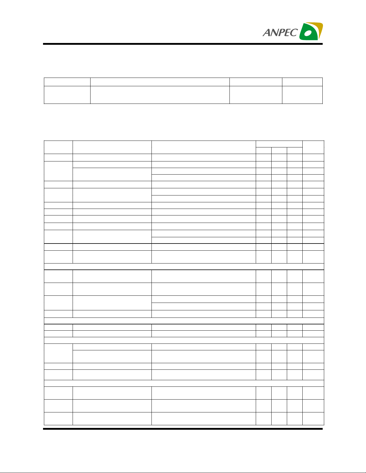
Electrical Characteristics
T
=25°C, V
A
Symbol Parameter Test Conditions
VIN Input Voltage
V
OUT
IQ Quiescent Current
I
GND
IL Output Load Current 150 mA
I
LIMIT
µV
µV
VIN-V
CL
I
REV
Enable Input
VIL
VIH
IEN Enable Input Current
Thermal Protection
TSD Thermal Shutdown 150 °C
T
SDHYS
Power Good
V
POK
VOL VO Out of Regulation Fault Condition,IOL=2mA,VIN=3.3V 0.13 0.15 V
I
POK
Switching Characteristics
t
STEP
Copyright ANPEC Electronics Corp.
Rev. A.4 - Aug., 2003
=5V, V
I
(EN)
=VI, I
=100µA, CL=1µF, unless otherwise specified.
O
APL5158
Min. Typ. Max.
2.7
Output Voltage IO=25mA 1.2 V
Output Voltage Accuracy
Ground Terminal Current
IO=0mA -1.0 +1.0 %
=1~150mA,TA=0°C to 70°C -2.0 +2.0 %
I
O
Ø0.8V
V
(EN)
I
=0mA
O
=150mA
I
O
0.45 1
60
370
Output Current Limit 300 600 m A
Line Regulation V
LNR
Load Regulation I
LDR
Dropout Voltage
OUT
=2.7V to 6V
IN
=10mA to 150mA
O
I
=100µA
O
=150mA 1.5 V
I
O
-0.1 +0.1
0.2 1
1.5
Load Capacitance ESR and Capacitance Tradeoffs 1
Reverse Output Current on
V
IN
Enable Input Logic-Low
Voltage
Enable Input Logic-High
Voltage
Resistance Discharge
=GND, V
IN
=2.7V to 6V Regulated Shutdown
V
IN
=2.7V to 6V Regulated Enabled
V
IN
Shutdown, V
Enabled, V
0.8V
V
Ø
EN
= Regulated Voltage
OUT
Ø0.8V
IL
Ù2V
IH
0.4
1.6
0.01
0.01
500
V
Hysteresis 15 °C
Low Threshold Output Falls % of V
High Threshold
Output Reaches % of V
Timer(Power OK)
POK Leakage Current Power good off,VIN=5V
Power Up Overshoot Max Voltage Overshoot Allowed on
(Power not OK) 83 %
OUT
,Starts Delay
O
90
1
1 %
Output During Power Up
Output Transient Time Limit Time for Output to Return within
5
Specified Regulation Range
Output Transient Voltage
Limit
Voltage that Load Step can Affect the
Nominal Output Voltage
1 %
www.anpec.com.tw3
Unit
6 V
µA
µA
µ
A
%
%
V
µF
4 mA
V
V
µA
µA
Ω
%
µA
µs
APL5158
Electrical Characteristics Cont.
T
=25°C, V
A
Symbol Parameter Test Conditions
ISR Load Step Current Slew
V
POK
Delay
Note 1 : Positive output current means the regulator is sourcing load current, and negative one is sinking
load current.
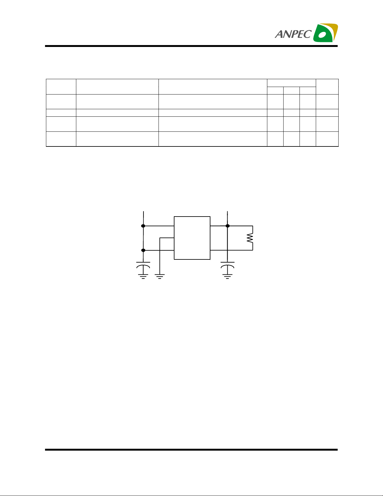
Application Circuit
=5V, V
I
Rate
(EN)
=VI, I
=100µA, CL=1µF, unless otherwise specified.
O
IL=10mA to 150mA
APL5158
Min. Typ. Max.
10
Unit
mA/µs
tr Power Up Rise Time 3 ms
tf Power Down Fall Time
Delay Time to Power Good 1 2.5 5 ms
VIN=3 to 6V
Discharge resistance=500Ω,
V
<1.08V
O
V
=1.2V
OUT
60
µs
1µF
1
V
IN
2
GND
3
EN POK
APL5158
5
V
OUT
4
10KΩ
1µF
Typical Application For Processor VID Code Power Sequencing Schematic
Copyright ANPEC Electronics Corp.
Rev. A.4 - Aug., 2003
www.anpec.com.tw4
APL5158
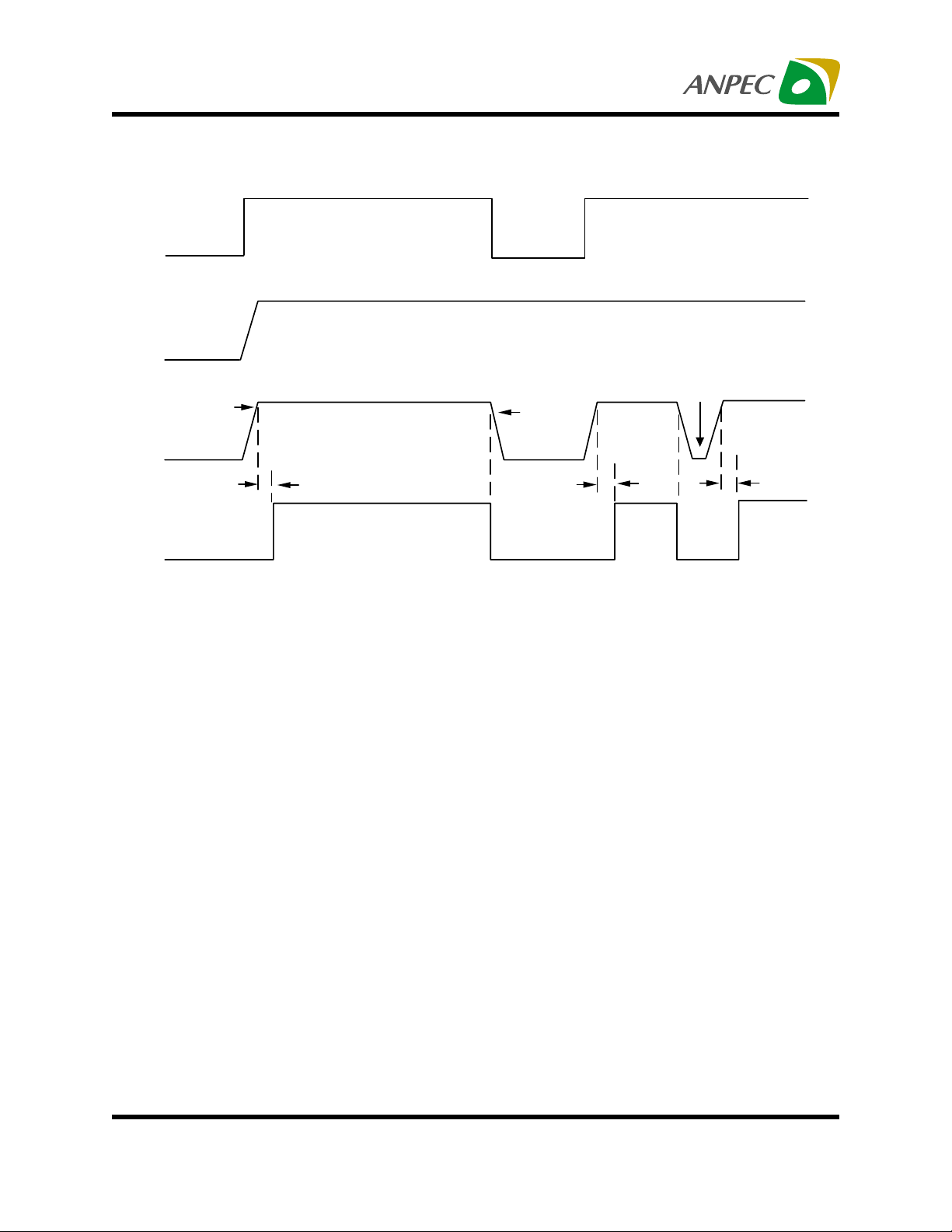
Timing Chart
EN
V
I
90% max
V
O
Fault Condition
83% min
2.5ms 2.5ms
POK Delay 2.5 ms typ.
POK
Copyright ANPEC Electronics Corp.
Rev. A.4 - Aug., 2003
www.anpec.com.tw5

APL5158
Typical Characteristics
Current Limit vs. lnput Voltage
700
600
500
400
300
200
Current Limit (mA)
100
0
3 3.5 4 4.5 5 5.5 6
Input Voltage (V)
POK Delay Time vs. Input Voltage
Ground Pin Current vs. Output Current
"
!#
!
#
#
#
Ground Pin Current (uA)
# # %# # #
VIN = 5V
Output Current (mA)
POK Sink Current vs. POK Low Voltage
#
"
IOL = 100uA
!
POK Delay Time (ms)
!"#$
Input Voltage (V)
Copyright ANPEC Electronics Corp.
Rev. A.4 - Aug., 2003
20
16
12
8
4
VIN = 3.3 V
POK is connected to VIN
POK Sink Current (mA)
0
00.511.522.533.5
POK Low Voltage (V)
www.anpec.com.tw6

APL5158
Typical Characteristics
EN Threshold Voltage vs. lnput Voltage
1.6
1.4
High Thershold
1
Low Thershold
0
23456
EN Threshold Voltage (V)
1.2
0.8
0.6
0.4
0.2
lnput Voltage (V)
Load Transient Response
Ground Pin Current vs. Input Voltage
IOUT =0mA
#
#
Ground Pin Current (uA)
!"#$
Input Voltage (V)
Line Transient Response
VOUT (10mV/div)
IOUT = 0.1mA to 150mA
(10mA /µs)
Time (20us/div) Time (20us / div)
Copyright ANPEC Electronics Corp.
Rev. A.4 - Aug., 2003
VIN = 3.3V
VIN = 3V to 4V
VOUT (20 mV/div)
www.anpec.com.tw7

APL5158
Typical Characteristics
Region of Stable COUT ESR vs. Output Current
10
VOUT = 1.2V
1
0.1
COUT = 1uF
Stable Region
COUT ESR(Ω)
0.01
Untested Region
0.001
0 50 100 150
Output Current (mA)
Power Down
Power Up
VIN (2V/div)
VOUT(0.5V/div)
POK(0.5V/div)
Time (2ms/div)
Exiting Shutdown
POK(0.5V/div)
Time (50ms/div)
Copyright ANPEC Electronics Corp.
Rev. A.4 - Aug., 2003
EN (2V/div)
VIN (2V/div)
VOUT(0.5V/div)
VOUT(0.5V/div)
POK(0.5V/div)
Time (2ms/div)
www.anpec.com.tw8

APL5158
Typical Characteristics
1.202
VIN =3.3V
1.200
POK Delay Time vs. TemperatureOutput Voltage vs. Temperature
4
VIN =3.3V
3.8
Output Voltage (V)
1.198
1.196
1.194
1.192
1.190
1.188
-40 -20 0 20 40 60 80 100 120
Temperature (°C)
Quiescent Current vs. Temperature
90
80
VIN =5V
70
IOUT =0mA
3.6
3.4
3.2
POK Delay Time (ms)
3
2.8
-40-20 0 20406080100
Temperature (°C)
60
50
VIN =3.3V
40
Quiescent Current (uA)
30
-40 -20 0 20 40 60 80 100 120
Temperature (°C)
Copyright ANPEC Electronics Corp.
Rev. A.4 - Aug., 2003
www.anpec.com.tw9

APL5158
Application Information
Capacitor Selection and Regulator
Stability
The APL5158 use at least a 1uF capacitor on the
input. This capacitor can use Aluminum, Tantalum or
Ceramic capacitors. Input capacitor with large value
and low ESR provides better PSRR and line-transient
response. The output capacitor also can use
Aluminum, Tantalum or Ceramic capacitors, and its
minimum values is recommended 1uF, ESR muse be
above 0.01Ω. The Curve of the region of stable C
ESR vs. load current in Typical Characteristics shows
the output capacitor ESR and load current range for
APL5158 stability. Large output capacitor values can
reduce noise and improve load-transient response,
stability, and PSRR. Note that some ceramic dielec-
trics exhibit large capacitance and ESR variation with
Temperature. If use this capacitor, it may be neces-
sary to use 2.2uF or more to ensure stability at tem-
perature below -10°C.
OUT
Power Ok
The power ok function monitors the output voltage
and drives high or low to indicate a fault. When a
fault condition such as overcurrent, undervoltage, ther-
mal shutdown., or dropout occurs, the power ok out-
put is pulled low. The power ok output comes back
when the output voltage has reached 90% of its nomi-
nal value and with a typ. 2.5ms delay time. The power
ok is an open-drain output, connect a 10kΩ resis-
tance to VOUT for typical application
Input-Output (Dropout)Voltage
The minimun input-output voltage differential (dropout)
determines the lowest usable supply voltage. The mini-
mum input voltage is 2.7V and output voltage is 1.2V,
so the dropout voltage is 1.5V.
Rev erse Protection
Load-Transient Considerations
The APL5158 Load-transient response graphs in Typi-
cal Characteristics show the transient response. A
step change in the load current from 0.1mA to 150mA
at 15u second will cause less than 10mV transient
spike. Large output capacitors value and low ESR
can reduce transient spike.
Shutdown/Enable
The APL5158 has an active high enable function.
Force EN high (>1.6V) enables the regulator, EN low
(<0.4V) disables the regulator and enter the shut-
down mode, it also causes the output voltage to dis-
charge through a 500Ω resistance to ground. In shut-
down mode, the quiescent current can reduce below
1uA. The EN pin cannot be floating, a floating EN pin
may cause an indeterminate state on the output. If it
is no use, connect to VIN for normal operation.
Copyright ANPEC Electronics Corp.
Rev. A.4 - Aug., 2003
The APL5158 has a internal reverse protection, it
doesnt need a external schottky diode to connect the
regulator input and output. If the output voltage is
forced above the input voltage, the IC will be shut-
down and the reverse output current is below 4mA , it
will increase with the output voltage. The maximum
allowable output voltage is 7V (see Absolute Maxi-
mum Rantings).
Current Limit
The APL5158 has a current limit protection, which
senses the current flows the P-channel MOSFET, and
controls the output voltage. The point where limiting
occurs is IOUT=600mA and the output voltage will be
shutdown. The output can be shorted to ground for
an indefinite amount of time without damaging the
part.
www.anpec.com.tw10

APL5158
Application Information
Thermal Protection
Thermal protection limits total power dissipation in the
APL5158. When the junction temperature exceeds
T
=+150°C, the thermal sensor generate a logic sig-
J
nal to turn off the pass transistor and let IC to cool.
When the ICs junction temperature cools by 15°C,
the thermal sensor will turn the pass transistor on
again, resulting in a pulsed output during continuous
thermal protection. Thermal protection is designed to
protect the IC in the event of fault conditions. For
continual operation, do not exceed the absolute maxi-
mum junction temperature rating of T
Operating Region and Power Dissi-
=+150°C.
J
pation
The thermal resistance of the case and circuit board,
ambient and junction air temperature, and the rate of
air flow all control the APL5158s maximum power
dissipation. The power dissipation across the device
is P = I
OUT (VIN-VOUT
tion is:
P
where TJ-TA is the temperature difference between
the junction and ambient air. θJB(or θ
resistance of the package, θ
tance through the printed circuit board, copper
traces, and other materials to the surrounding air.
The GND pin of the APL5158 provide an electrical
connection to ground and channeling heat away.
Connect the GND pin to ground using a large pad or
ground plane as a heatsink, it can improve maximize
thermal dissipation.
). The maximum power dissipa-
MAX
= (TJ-T
) / (θJB +θ
A
is the thermal resis-
BA
)
BA
) is the thermal
JB
Copyright ANPEC Electronics Corp.
Rev. A.4 - Aug., 2003
www.anpec.com.tw11

APL5158
Packaging Information
SOT-23-5
e1
45
12
3
E1 E
e
D
Dim
Min. Max. Min. Max.
A 0.95 1.45
A1 0.05 0.15
A2 0.90 1.30
D2.83.00
E2.63.00
E1 1.5 1.70
L 0.35 0.55
b
A2
A1 L 2
A
L
a
Millimeters Inches
0.037 0.057
0.002 0.006
0.035 0.051
0.110 0.118
0.102 0.118
0.059 0.067
0.014 0.022
L 1
L1 0.20 BSC 0.008 BSC
L2 0.5 0.7
0.020 0.028
N5 5
α
0
°
10
°
0
°
10
°
Copyright ANPEC Electronics Corp.
Rev. A.4 - Aug., 2003
www.anpec.com.tw12

APL5158
Physical Specifications
Terminal Material Solder-Plated Copper (Solder Material : 90/10 or 63/37 SnPb)
Lead Solderability Meets EIA Specification RSI86-91, ANSI/J-STD-002 Category 3.
Reflow Condition (IR/Convection or VPR Reflow)
Reference JEDEC Standard J-STD-020A APRIL 1999
Peak temperature
temperature
Pre-heat temperature
°
183 C
Time
Classification Reflow Prof iles
Convection or IR/
Convection
Average ramp-up rate(183°C to Peak) 3°C/second max. 10 °C /second max.
Preheat temperature 125 ± 25°C)
Temperature maintained above 183°C
Time within 5°C of actual peak temperature
Peak temperature range
Ramp-down rate
Time 25°C to peak temperature
120 seconds max
60 150 seconds
10 20 seconds 60 seconds
220 +5/-0°C or 235 +5/-0°C 215-219°C or 235 +5/-0°C
6 °C /second max. 10 °C /second max.
6 minutes max.
VPR
Package Reflow Conditions
pkg. thickness
and all bgas
Convection 220 +5/-0 °C Convection 235 +5/-0 °C
VPR 215-219 °C VPR 235 +5/-0 °C
IR/Convection 220 +5/-0 °C IR/Convection 235 +5/-0 °C
Copyright ANPEC Electronics Corp.
Rev. A.4 - Aug., 2003
2.5mm
≥≥≥≥
pkg. thickness < 2.5mm and
pkg. volume
350 mm³
≥≥≥≥
pkg. thickness < 2.5mm and pkg.
volume < 350mm³
www.anpec.com.tw13

APL5158
R e lia bilit y te s t pr o g ra m
SOLDERABILITY MIL-STD-883D-2003
HOLT MIL-STD-883D-1005.7
PCT JESD-22-B, A102
TST MIL-STD-883D-1011.9
245°C , 5 S EC
1000 Hrs Bias @ 125 °C
16 8 H rs, 100 % R H , 12 1°C
-65°C ~ 150°C , 20 0 C yc les
ESD MIL-STD-883D-3015.7 VHBM > 2KV, VMM > 200V
La tch-Up JE SD 78 10 m s , Itr > 100m A
Test item Method Description
Carrier Tape
W
E
F
Po
P
P1
Ao
D
Bo
D1
T2
t
Ko
A
Application
A B C J T1 T2 W P E
178±172 ± 1.0 13.0 + 0.2 2.5 ± 0.15 8.4 ± 2 1.5± 0.3
SOT-23-5
F D D1 Po P1 Ao Bo Ko t
3.5 ± 0.05 1.5 +0.1 1.5 +0.1 4.0 ± 0.1 2.0 ± 0.1 3.15 ± 0.1 3.2± 0.1 1.4± 0.1 0.2±0.03
Copyright ANPEC Electronics Corp.
Rev. A.4 - Aug., 2003
J
C
B
T1
8.0+ 0.3
- 0.3
4 ± 0.1 1.75± 0.1
www.anpec.com.tw14

APL5158
Cover Tape Dimensions
Application Carrier Width Cover Tape Width Devices Per Reel
SOT- 23
Customer Service
Anpec Electronics Corp.
Head Office :
5F, No. 2 Li-Hsin Road, SBIP,
Hsin-Chu, Taiwan, R.O.C.
Tel : 886-3-5642000
Fax : 886-3-5642050
Taipei Branch :
7F, No. 137, Lane 235, Pac Chiao Rd.,
Hsin Tien City, Taipei Hsien, Taiwan, R. O. C.
Tel : 886-2-89191368
Fax : 886-2-89191369
8 5.3 3000
Copyright ANPEC Electronics Corp.
Rev. A.4 - Aug., 2003
www.anpec.com.tw15
 Loading...