

APL5156
High Input Voltage, Low Quiescent Current, 150mA LDO Regulator
Features
• Wide Operating Voltage : 6.5V~25V
• Ultra Low Ground Current : 70µA
• High Output Accuracy : ±2% Over Temperature
• Excellent Load/Line Transient
• Low Dropout Voltage : 1900mv @ 150mA
• Fixed Output Voltages for 5V/3.3V or Adjustable
Voltage
• Built-In Reverse Battery Protection
• Built-In Reverse Leakage Protection
• Built-In Current-Limit Protection
• Built-In Over-Temperature Protection
• Zero Shutdown Current
• Internal Soft-Start Function 0.5ms~1.5ms (max)
Over Temperature
• POR Scheme to Prevent V
OUT
Spike
• Stable with Aluminum, Tantalum, or Ceramic
Capacitors
• SOT-23-5, SOT-89, and SOP-8P Packages
• Lead Free and Green Devices Available
(RoHS Compliant)
Applications
• USB Power Supply
• Keep-Alive Supply in Notebook and Portable
Computers
• Logic Supply for High-Voltage Batteries
• Battery Powered Systems
General Description
The APL5156 is a low ground current linear regulator,
which operates with input voltage from 6.5V to 25V and
delivers output current up to 150mA. Typical dropout voltage is only 1.9V at 150mA loading. This combination of
the high voltage and the low ground current makes the
APL5156 ideal for USB and portable devices, using 2cell or 3-cell Li-Ion battery inputs.
The APL5156 is stable with aluminum, tantalum, and
ceramic capacitors. It requires a 2.2µF or greater capacitor for stability.
The APL5156 has many protection functions, including
over-temperature, current-limit, reverse battery, and
reverse leakage protections which prevent the device from
thermal over-load, current over-load, reverse connection
of the battery and output current reversing to the VIN.
The APL5156 regulator is available in miniature SOT-235, SOT-89, and SOP-8P packages.
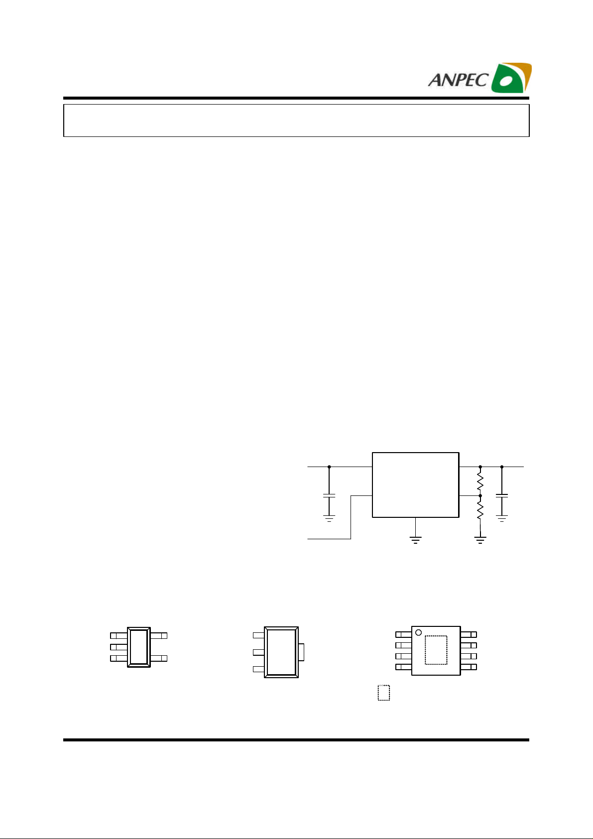
Simplified Application Circuit
VIN
C
IN
1µF
Adjustable Output Voltage (SOT-23-5/SOP-8P)
APL5156
EN
GND
VOUT
ADJ
C
OUT
2.2µF
Pin Configuration
SOT-23-5
VIN 1
GND 2
EN 3
ANPEC reserves the right to make changes to improve reliability or manufacturability without notice, and
advise customers to obtain the latest version of relevant information to verify before placing orders.
Copyright ANPEC Electronics Corp.
Rev. A.6 - Oct., 2009
5 VOUT
4 NC/ADJ
GND 1
VIN 2
VOUT 3
SOT-89
TAB: VIN
VOUT 1
NC 2
NC 3
NC/ADJ 4
SOP-8P
8 VIN
7 GND
6 NC
5 EN
Thermal Pad (connected to GND
plane for better dissipation)
www.anpec.com.tw1
APL5156
Ordering and Marking Information
APL5156
Assembly Material
Handling Code
Temperature Range
Package Code
Voltage Code
APL5156 B :
APL5156 33B :
APL5156 50B :
APL5156 D :
APL5156 KA :
Note: ANPEC lead-free products contain molding compounds/die attach materials and 100% matte tin plate termination finish; which
are fully compliant with RoHS. ANPEC lead-free products meet or exceed the lead-free requirements of IPC/JEDEC J-STD-020D for
MSL classification at lead-free peak reflow temperature. ANPEC defines “Green” to mean lead-free (RoHS compliant) and halogen
free (Br or Cl does not exceed 900ppm by weight in homogeneous material and total of Br and Cl does not exceed 1500ppm by
weight).
L56X
56RX
56ZX
APL5156
XXXXX33
APL5156
XXXXX
Package Code
B : SOT-23-5 D : SOT-89 KA : SOP-8P
Operating Ambient Temperature Range
I : -40 to 85 oC
Handling Code
TR : Tape & Reel
Voltage Code :
33 : 3.3V 50 : 5.0V Blank : Adjustable Version
Assembly Material
G : Halogen and Lead Free Device
X - Date Code
X - Date Code ; 33 - 3.3V
X - Date Code ; 50 - 5.0V
XXXXX - Date Code ; 33 - 3.3V
XXXXX - Date Code
Absolute Maximum Ratings (Note 1)
Symbol Parameter Rating Unit
VIN,VEN VIN, EN to GND Voltage - 27 to 27 V
EN to VIN Voltage -27 to 27 V
V
Note 1: Absolute Maximum Ratings are those values beyond which the life of a device may be impaired. Exposure to absolute
maximum rating conditions for extended periods may affect device reliability.
VOUT, ADJ to GND Voltage - 0.3 to 27 V
OUT,VADJ
VOUT, ADJ to VIN Voltage -27 to 27 V
PD Power Dissipation Internally Limited W
TJ Operating Junction Temperature -40 to 125
T
Storage Temperature Range -65 to +150
STG
T
Maximum Lead Soldering Temperature, 10 Seconds 260
SDR
o
o
o
Thermal Characteristics
Symbol Parameter Typical Value Unit
Thermal Resistance-Junction to Ambient
θJA
Copyright ANPEC Electronics Corp.
Rev. A.6 - Oct., 2009
(Note 2)
SOT-23-5
SOT-89
SOP-8P
235
180
50
o
C/W
www.anpec.com.tw2
C
C
C
APL5156
Thermal Characteristics (Cont.)
Symbol Parameter Typical Value Unit
Thermal Resistance-Junction to Case
θJC
SOT-89
SOT-23-5
SOP-8P
Note 2: θ
is measured with the component mounted on a high effective thermal conductivity test board in free air.
JA
Electrical Characteristics
Unless otherwise noted, these specifications apply over VIN=V
to TA=25oC.
Symbol Parameter Test Conditions
VIN Input Voltage
V
Output Voltage Accuracy -2 - 2 %
OUT
Output Voltage Range 3 - 20 V
I
OUT
I
IQ Quiescent Current
I
Load Current Range 0 - 150 mA
OUT
V
Reference Voltage -2% 1.24 +2% V
REF
REG
Line Regulation V
LINE
REG
Load Regulation 0.1mA<I
LOAD
V
Dropout Voltage
DROP
I
I
I
I
I
I
OUT
OUT
OUT
OUT
OUT
OUT
OUT
OUT
POWER-ON-RESET (POR)
Rising VIN Threshold 4 5 6 V
PROTECTIONS
Over-Temperature Shutdown - 150 -
OTS
I
LIMIT
I
SHORT
Over-Temperature Shutdown
Hysteresis
Circuit Current Limit VIN =V
Short Current V
Output Leakage,
Reverse Polarity Input
- 10 -
OUT
Load=500Ω,VIN= -15V, EN=GND
Load=500Ω, VIN=VEN= -15V
SOFT-START AND SHUTDOWN
TSS Soft-Start Interval From enable to V
VEN
Input High Voltage 2.5 - Input Low Voltage
IEN EN Pin Input Bias Current VEN=25V - 1 5
I
Shutdown Supply Current EN=Low, VIN=19V - 0.1 1
QSHDN
+2.5V, CIN=1µF, C
OUT
=2.2µF, TA=-40oC to 85oC. Typical values refer
OUT
Min. Typ. Max.
6.5 - 25 V
=0.1mA - 70 100
=50mA - 0.5 1 mA
=100mA - 2 3.5 mA
=150mA - 5 7 mA
+2.5V<VIN<25V, I
<150mA - 0.4 1 %
OUT
=1mA - 0.01 - %
OUT
=0.1mA - 1300 1900
=50mA - 1600 2000
=100mA - 1700 2100
=150mA - 1900 2300
+2.5V 250 350 500 mA
OUT
=0V - 50 - mA
- -3 -5
- -4 -5 mA
= 90% 0.5 1 1.5 ms
OUT
- - 0.6
130
38
20
APL5156
o
C/W
Unit
mV
µA
o
C
oC
µA
V
µA
µA
Copyright ANPEC Electronics Corp.
www.anpec.com.tw3
Rev. A.6 - Oct., 2009
APL5156
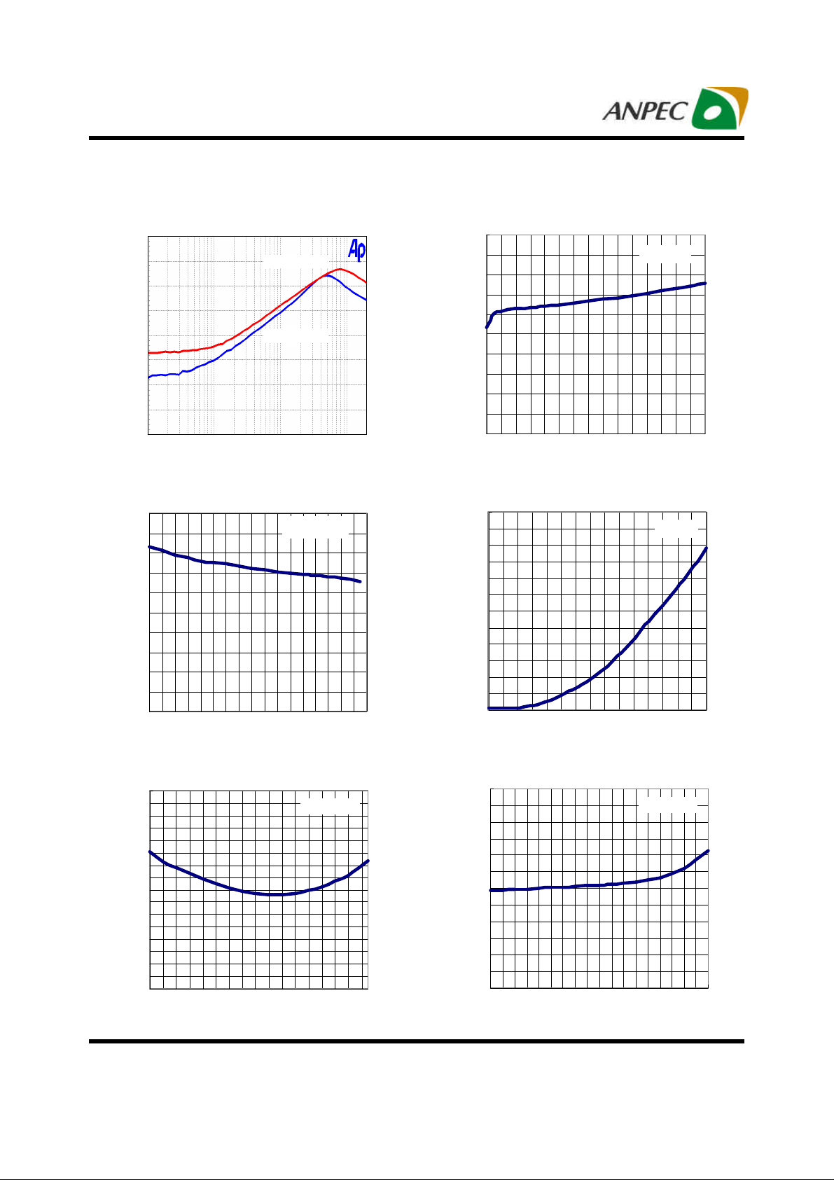
Typical Operating Characteristics
PSRR vs. Frequency
0
IOUT=100mA
-20
-40
IOUT=10mA
PSRR (dB)
-60
-80
10 100 1K 10K 100K
Frequency (Hz)
Dropout Voltage vs. Temperature
2.5
2
1.5
1
Dropout Voltage (V)
0.5
I
OUT
=150mA
Dropout Voltage vs. Output Current
2.5
2
1.5
1
Dropout Voltage (V)
0.5
0
0 20 40 60 80 100 120 140
Output Current (mA)
Quiescent Current vs. Output Current
6000
5000
4000
3000
2000
Quiescent Current (µA)
1000
TA=25°C
VIN=6V
0
-40 -20 0 20 40 60 80 100 120
Temperature (oC)
Quiescent Current vs. Temperature
90
85
80
75
70
65
60
Quiescent Current (µA)
55
50
-40 -20 0 20 40 60 80 100 120
Temperature (oC)
Copyright ANPEC Electronics Corp.
Rev. A.6 - Oct., 2009
I
OUT
=10mA
0
0 20 40 60 80 100 120 140
Output Current (mA)
Quiescent Current vs. Input Voltage
100
90
80
70
60
Quiescent Current (µA)
50
40
6 8 10 12 14 16 18 20 22 24
Input Voltage (V)
I
=10mA
OUT
www.anpec.com.tw4
APL5156
Typical Operating Characteristics (Cont.)
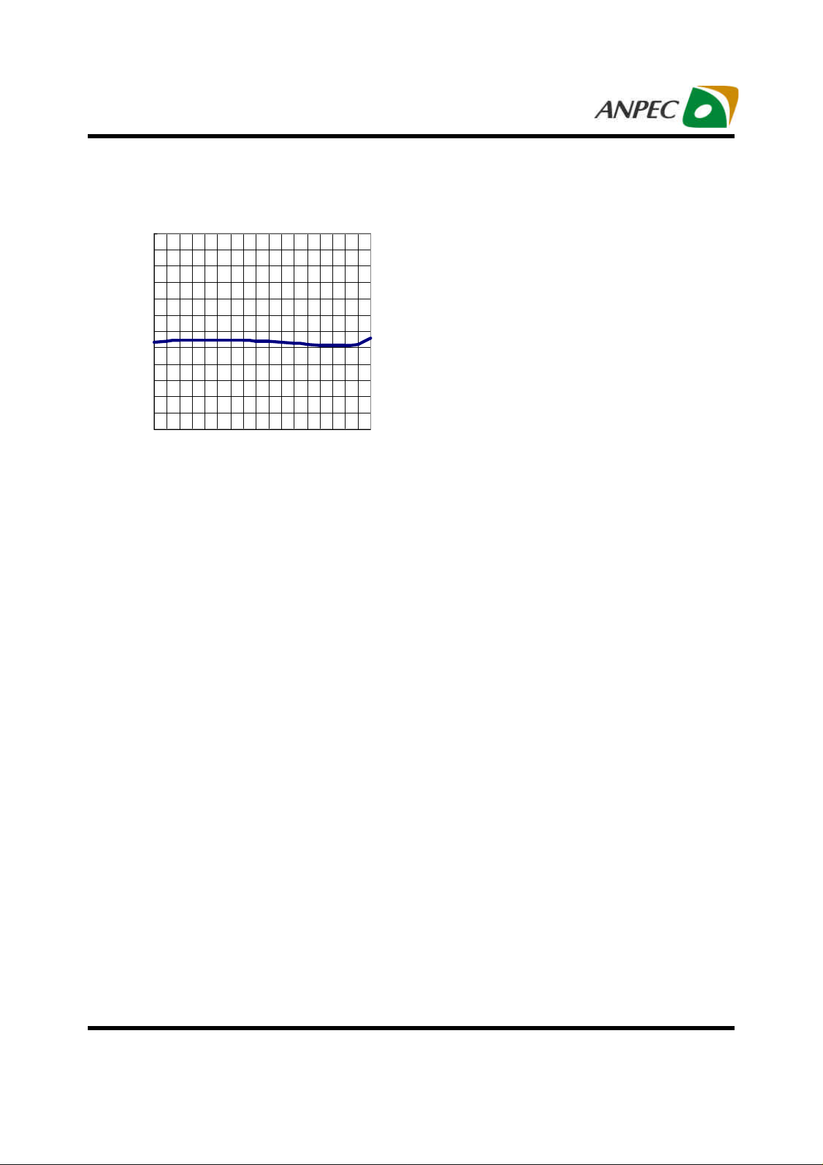
Output Voltage vs. Temperature
3.4
3.35
3.3
3.25
3.2
Output Voltage (V)
3.15
3.1
-20
-40
0 20 40 60 80 100 120
Temperature (oC)
Copyright ANPEC Electronics Corp.
Rev. A.6 - Oct., 2009
www.anpec.com.tw5
APL5156
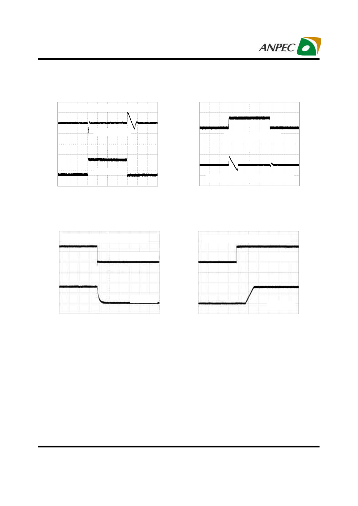
Operating Waveforms
Load Transient Line Transient
VIN=12V ; V
=3.3V ; CIN=1µF ; C
OUT
V
OUT
I
(1~150mA)
OUT
Time (50µs/div)
Entering Shutdown Delay
VIN=6V ; CIN=1µF ; C
OUT
(100mV/div)
=2.2µF ; I
OUT
OUT
=100mA
=2.2µF
VEN(2V/div)
VIN=11.5V~12.5V ; TR=1µs
V
(200mV/div) ; C
OUT
=2.2µF ; I
OUT
Time (50µs/div)
Exiting Shutdown Waveform
VIN=6V ; CIN=1µF ; C
=2.2µF ; I
OUT
=10mA
OUT
=100mA
OUT
VEN(2V/div)
Time (0.5ms/div)
Copyright ANPEC Electronics Corp.
Rev. A.6 - Oct., 2009
V
OUT
(2V/div)
Time (0.5ms/div)
V
OUT
www.anpec.com.tw6
(2V/div)

APL5156
Pin Description
PIN
NO.
SOT-23-5 SOT-89 SOP-8P
NAME
1 2 8 VIN Voltage supply input pin
2 1 7 GND Ground
3 - 5 EN Enable pin, Logic low=shutdown; Logic high=enable
4 - 4 NC/ADJ
NC: No Connection
ADJ: Output voltage feedback pin
5 3 1 VOUT Regulator out put pin
Block Diagram
FUNCTION
VIN
EN
ENABLE
V
REF
Adjustable Output Voltage (SOT-23-5/SOP-8P)
VIN
EN
ENABLE
GND
VOUT
R
1
ADJ
R
2
VOUT
R
1
V
REF
R
2
Fixed Output Voltage (SOT-23-5/SOP-8P)
Copyright ANPEC Electronics Corp.
GND
www.anpec.com.tw7
Rev. A.6 - Oct., 2009

APL5156
Block Diagram (Cont.)
VIN
V
REF
Fixed Output Voltage (SOT-89)
Typical Application Circuit
C
IN
1µF
VIN
EN
GND
GND
VOUT
ADJ
R
R
C
OUT
2.2µF
VOUT
1
2
Enable signal
1µF
Enable signal
1µF
Copyright ANPEC Electronics Corp.
Rev. A.6 - Oct., 2009
Adjustable Output Voltage (SOT-23-5/SOP-8P)
VIN
C
IN
EN
VOUT
NC
GND
Fixed Output Voltage (SOT-23-5/SOP-8P)
VIN
C
IN
VOUT
GND
Fixed Output Voltage (SOT-89)
C
OUT
2.2µF
C
OUT
2.2µF
www.anpec.com.tw8
APL5156
Application Information
Enable/Shutdown
The APL5156 features an active-high enable pin that allows the regulator to be disabled. Forcing the enable pin
low disables the regulator, so current consumed by the
regulator goes nearly to zero. Forcing the enable pin high
enables the output voltage. The enable pin can not float.
Input Capacitor
The APL5156 has high input voltage up to 25V. The input
capacitor must be rated to sustain voltages that may be
used on the input. An input capacitor may be required
when the device is not near the source power supply or
when supplied by a battery. Small and surface-mounted
ceramic capacitors can be used for bypassing. A larger
value may be required if the source supply has high ripple.
TT
−
P
=
)MAX(D
AJ
θ
JA
where TJ-TA is the temperature difference between the
junction and ambient air. θJA is the thermal resistance
between junction and ambient air.
For continual operation, do not exceed the absolute maximum junction temperature rating of TJ=125oC.
For example:
In SOT-23-5 package θJA=235oC/W. When operates the
APL5156 at TA=50oC, the maximum power dissipation
can be determined as below:
P
=(125oC-50oC)/(235oC/W)
D(MAX)
P
=319.1mW
D(MAX)
Output Capacitor
The APL5156 requires an output capacitor for stability.
The design requires 2.2µF or greater on the output to
maintain stability. It is optimized by using low-ESR ceramic chip capacitors. The maximum allowable ESR is
3Ω. More capacitance improves transient response. Place
the output capacitor as close to the VOUT pin as possible.
X7R/X5R dielectric-type ceramic capacitors are recommended because of their temperature performance. X7R
type capacitors change capacitance by 15% over their
operating temperature ranges. To use a ceramic chip
capacitor with Y5V dielectric, the value must be much
higher than an X7R ceramic capacitor to ensure the same
minimum capacitance over the equivalent operating temperature range.
No-Load Stability
The APL5156 will remain stable and in regulation with no
load unlike many other voltage regulators. This is especially important in CMOS RAM keep-alive applications.
Thermal Consideration
Thermal Pad Consideration
The SOP-8P is a cost-effective package which features a
small size, like a standard SOP-8, and a bottom thermal
pad to minimize the thermal resistance of the package is
applicable to high current applications. The thermal pad
must be soldered down to the copper plane on circuit
board. Heat can be conducted away from the thermal
pad through the copper plane to ambient. If the copper
plane is not on the top surface of the circuit board, 4 or 6
vias should be used to thermally couple the thermal pad
to the bottom plane.
For good thermal conduction, the vias must be plated
through and solder filled. The copper plane used to conduct heat away from the thermal pad should be as large
as practical.
0.072
0.150
0.118
0.024
The thermal resistance of junction to ambient controls
the APL5156's maximum power dissipation. The power
dissipation across the device is PD=I
OUT (VIN-VOUT
), and the
maximum power dissipation is :
Copyright ANPEC Electronics Corp.
Rev. A.6 - Oct., 2009
0.212
SOP-8P Layout Recommendation
www.anpec.com.tw9
ground
plane for
thermal
pad

APL5156
Application Information (Cont.)
Adjustable Regulator Application
The output voltage of APL5156 can be adjusted from 3V
to 20V by using two external resistors. The resistors set
the output voltage based on the following equation:
R
1
+=
R
2
where V
REF
REFOUT
=1.24V
1VV
Feedback resistor R2 should be larger than 100kΩ and
smaller than 1MΩ. The resistors should be placed as
close the device as possible to avoid noise.
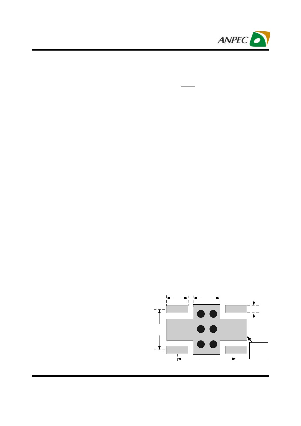
Recommended Minimum Footprint
SOT-23-5
0.076
0.1
SOP-8P
8 7 6 5
0.138
0.212
1 2 3 4
0.050
0.024
0.072
0.118
Unit : Inch
0.038
0.02
Unit : Inch
SOT-89
0.076
0.140
0.104
0.059
Copyright ANPEC Electronics Corp.
Rev. A.6 - Oct., 2009
0.022
Unit : Inch
0.05
0.067
www.anpec.com.tw10

APL5156
Pack age Information
SOT-23-5
D
e
b c
e1
SEE
VIEW A
E1
E
A
A2A1
L
VIEW A
0.25
GAUGE PLANE
SEATING PLANE
0
MAX.
1.45
0.15
1.30
0.50
0.22
3.00
1.80
0.60
8
SOT-23-5
MIN.
0.000
0.035
0.003
0.106
0.055
0.012
0
INCHES
MAX.
0.057
0.006
0.051
0.0200.012
0.009
0.122
0.1180.102
0.071
0.037 BSC
0.075 BSC
0.024
8
S
Y
M
B
O
L
A
A1
A2
b
c
D
E
E1
e
e1
L
0
Note : 1. Follow JEDEC TO-178 AA.
2. Dimension D and E1 do not include mold flash, protrusions or gate
burrs. Mold flash, protrusion or gate burrs shall not exceed 10 mil
per side.
MILLIMETERS
MIN.
0.00
0.90
0.30
0.08
2.70
2.60
1.40
0.95 BSC
1.90 BSC
0.30
0
3.10
Copyright ANPEC Electronics Corp.
Rev. A.6 - Oct., 2009
www.anpec.com.tw11

APL5156
Pack age Information
SOT-89
B1
S
Y
M
B
O
L
A
B
B1
C
D
D1
E
E1
e
e1
H
L 0.89
MIN. MAX.
1.40
0.44
0.36 0.48
0.35 0.44
4.40 4.60
1.62 1.83
2.29 2.60
2.13
3.94 4.25
D
D1
EL
H
e
e1
B
SOT-89
MILLIMETERS
1.60
0.56
2.29
1.50 BSC 0.059 BSC
3.00 BSC
1.20
E1
INCHES
MIN. MAX.
0.055
0.017
0.014 0.019
0.014 0.017
0.173 0.181
0.064 0.072
0.090 0.102
0.084
0.118 BSC
0.155 0.167
0.035
A
C
0.063
0.022
0.090
0.047
Copyright ANPEC Electronics Corp.
Rev. A.6 - Oct., 2009
Note : Follow JEDEC TO-243 AA.
www.anpec.com.tw12

APL5156
Pack age Information
SOP-8P
D
D1
SEE VIEW A
b
c
D
E
e
h
L
THERMAL
PAD
e
S
Y
M
B
O
L
A
A1
A2
D1
E1
0
Note : 1. Followed from JEDEC MS-012 BA.
2. Dimension "D" does not include mold flash, protrusions or gate burrs.
Mold flash, protrusion or gate burrs shall not exceed 6 mil per side .
3. Dimension "E" does not include inter-lead flash or protrusions.
Inter-lead flash and protrusions shall not exceed 10 mil per side.
MIN.
0.00
1.25
0.31
0.17
4.80 5.00
2.50
5.80 6.20
3.80 4.00
2.00
0.25
0.40
E2
b
MILLIMETERS
1.27 BSC
0oC
E
E1
o
h X 45
A
A2
A1
L
VIEW A
SOP-8P
MAX.
1.60
0.15
0.51
0.25
3.50
3.00
0.50
1.27
8oC 0oC 8oC
MIN.
0.000
0.049
0.012
0.007
0.189 0.197
0.098
0.228 0.244
0.150 0.157
0.079E2
0.010
0.016
c
0.25
GAUGE PLANE
SEATING PLANE
θ
INCHES
MAX.
0.063
0.006
0.020
0.010
0.138
0.118
0.050 BSC
0.020
0.050
Copyright ANPEC Electronics Corp.
Rev. A.6 - Oct., 2009
www.anpec.com.tw13

APL5156
Carrier Tape & R eel Dimensions
OD0
B0
P0
P2
P1
A
E1
F
W
Application
SOT-23-5
Application
SOT-89
Application
SOP-8P
K0
SECTION A-A
B
A
H
A0
SECTION B-B
OD1
B
T
A
d
T1
A H T1 C d D W E1 F
178.0±2.00 50 MIN.
8.4+2.00
-0.00
13.0+0.50
-0.20
1.5 MIN. 20.2 MIN. 8.0±0.30 1.75±0.10 3.5±0.05
P0 P1 P2 D0 D1 T A0 B0 K0
4.0±0.10 4.0±0.10 2.0±0.05
1.5+0.10
-0.00
1.0 MIN.
0.6+0.00
-0.40
3.20±0.20 3.10±0.20 1.50±0.20
A H T1 C d D W E1 F
178.0±2.00 50 MIN.
12.4+2.00
-0.00
13.0+0.50
-0.20
1.5 MIN. 20.2 MIN. 12.0±0.30 1.75±0.10 5.50±0.05
P0 P1 P2 D0 D1 T A0 B0 K0
4.0±0.10 8.0±0.10 2.0±0.05
1.5+0.10
-0.00
1.5 MIN.
0.6+0.00
-0.40
4.80±0.20 4.50±0.20 1.80±0.20
A H T1 C d D W E1 F
330.0±2.00 50 MIN.
12.4+2.00
-0.00
13.0+0.50
-0.20
1.5 MIN. 20.2 MIN. 12.0±0.30 1.75±0.10 5.5±0.05
P0 P1 P2 D0 D1 T A0 B0 K0
4.0±0.10 8.0±0.10 2.0±0.05
1.5+0.10
-0.00
1.5 MIN.
0.6+0.00
-0.40
6.40±0.20 5.20±0.20 2.10±0.20
Copyright ANPEC Electronics Corp.
Rev. A.6 - Oct., 2009
(mm)
www.anpec.com.tw14

APL5156
Devices Per Unit
Package Type Unit Quantity
SOT-23-5 Tape & Reel 3000
SOT-89 Tape & Reel 1000
SOP-8P
Taping Direction Information
SOT-23-5
Tape & Reel 2500
USER DIRECTION OF FEED
SOT-89
Copyright ANPEC Electronics Corp.
Rev. A.6 - Oct., 2009
USER DIRECTION OF FEED
www.anpec.com.tw15

APL5156
Taping Direction Information
SOP-8P
USER DIRECTION OF FEED
Classification Profile
Copyright ANPEC Electronics Corp.
Rev. A.6 - Oct., 2009
www.anpec.com.tw16

APL5156
Classification Reflow Profiles
Profile Feature Sn-Pb Eutectic Assembly Pb-Free Assembly
Preheat & Soak
Temperature min (T
Temperature max (T
Time (T
smin
to T
smax
smin
smax
) (ts)
)
)
Average ramp-up rate
(T
to TP)
smax
Liquidous temperature (TL)
Time at liquidous (tL)
Peak package body Temperature
(Tp)*
Time (tP)** within 5°C of the specified
classification temperature (Tc)
Average ramp-down rate (Tp to T
smax
Time 25°C to peak temperature
See Classification Temp in table 1 See Classification Temp in table 2
)
100 °C
150 °C
60-120 seconds
150 °C
200 °C
60-120 seconds
3 °C/second max. 3°C/second max.
183 °C
60-150 seconds
217 °C
60-150 seconds
20** seconds 30** seconds
6 °C/second max. 6 °C/second max.
6 minutes max. 8 minutes max.
* Tolerance for peak profile Temperature (Tp) is defined as a supplier minimum and a user maximum.
** Tolerance for time at peak profile temperature (tp) is defined as a supplier minimum and a user maximum.
Table 1. SnPb Eutectic Process – Classification Temperatures (Tc)
Package
Thickness
<2.5 mm
Volume mm
3
Volume mm
<350
235 °C 220 °C
≥350
3
≥2.5 mm 220 °C 220 °C
Table 2. Pb-free Process – Classification Temperatures (Tc)
Package
Thickness
<1.6 mm
1.6 mm – 2.5 mm
Volume mm3
<350
Volume mm3
350-2000
Volume mm3
260 °C 260 °C 260 °C
260 °C 250 °C 245 °C
>2000
≥2.5 mm 250 °C 245 °C 245 °C
Reliability Test Program
Test item Method Description
SOLDERABILITY JESD-22, B102
HOLT JESD-22, A108
PCT JESD-22, A102
TCT JESD-22, A104
HBM MIL-STD-883-3015.7
MM JESD-22, A115
Latch-Up JESD 78
Copyright ANPEC Electronics Corp.
Rev. A.6 - Oct., 2009
5 Sec, 245°C
1000 Hrs, Bias @ 125°C
168 Hrs, 100%RH, 2atm, 121°C
500 Cycles, -65°C~150°C
VHBM≧2KV
VMM≧200V
10ms, 1tr≧100mA
www.anpec.com.tw17

APL5156
Customer Service
Anpec Electronics Corp.
Head Office :
No.6, Dusing 1st Road, SBIP,
Hsin-Chu, Taiwan
Tel : 886-3-5642000
Fax : 886-3-5642050
Taipei Branch :
2F, No. 11, Lane 218, Sec 2 Jhongsing Rd.,
Sindian City, Taipei County 23146, Taiwan
Tel : 886-2-2910-3838
Fax : 886-2-2917-3838
Copyright ANPEC Electronics Corp.
Rev. A.6 - Oct., 2009
www.anpec.com.tw18

 Loading...