

ANPEC APL431LBYI-TR, APL431LBYI-TB, APL431LBYC-TR, APL431LBYC-TB, APL431LBYC-PB Datasheet
...
APL431L
Low Voltage Adjustable Precision Shunt Regulator
Features General Description
••
•
Precise Reference Voltage to 1.24V
••
••
•
Guaranteed 0.5% or 1% Reference Voltage
••
Tolerance
••
•
Sink Current Capability, 80uA to 100mA
••
••
•
Quick Turn-on
••
••
•
Adjustable Output Voltage, VO = V
••
••
• Low Operational Cathode Current, 80µA
••
to 20V
REF
Typical
••
• 0.1Ω Typical Output Impedance
••
••
• SOT-23-3, SOT-23-5, TO-92 and SOT-89
••
Packages
Applications
••
• Linear Regulators
••
••
• Adjustable Power Supply
••
••
• Switching Power Supply
••
The APL431L is a 3-terminal low voltage adjustable
precision reference with specified thermal stability
over applicable commercial temperature ranges. Output voltage may be set to any value between V
(1.
ref
24 V) and 20 V with two external resistors (see Figure 2). When used with an photocoupler, the
APL431L is an ideal voltage reference in isolated feedback circuits for 3V to 12V switching-mode power
supplies. This device has a typical output impedance of 0.1Ω. Active output circuitry provides a very
sharp turn-on characteristic, making the APL431L excellent replacements for zener diodes in many
applications, including on-board regulation and adjustable power supplies.
ANODE
3
12
REF
CATHODE
SOT-23-3 (Top View)
CATHODE3
ANODE
2
1
REF
REF
SOT-23-5 (Top View)
123
REF ANODE CATHODE
NC
NC
45
123
ANODE
CATHODE
Symbol
REF
CathodeAnode
ANPEC reserves the right to make changes to improve reliability or manufacturability without notice, and advise
customers to obtain the latest version of relevant information to verify before placing orders.
Copyright ANPEC Electronics Corp.
Rev. B.7 - May., 2003
TO-92 (Top View)
Functional Diagram
Cathode
REF
+
_
ref
V
Anode
SOT-89 (Top View)
www.anpec.com.tw1

APL431L
Ordering and Marking Information
APL431L
APL431L A/B :
APL431L D :
431L
APL431L
XXXXX
XXXXX
Handling Code
Temp. Range
Package Code
Elec. Grade
- Date Code
Elec. Grade
A : 0.5% Reference Voltage Tolerance
B : 1% Reference Voltage Tolerance
Package Code
A : SO T-23-3 B : SO T-23-5
D : SO T-89 E : TO -92
Y:Chip Form
Temp. Range
C : 0 to 70 C I : -40 to 85 C
Handling Code
PB : Plastic Bag TB : Tap e & Box
TR : Ta pe & Re el
APL431L E :
°
APL
431L
XXXXX
°
XXXXX - Date Code
Absolute Maximum Ratings
Symbol Parameter Rating Unit
V
KA
I
K
I
REF
θ
JA
T
J
T
STG
T
SOL
Cathode voltage
Continuous cathode current range
Reference current range
20 V
100 mA
3mA
Thermal Resistance from Junction to Ambient in Free Air
SOT-23-3
SOT-23-5
SOT-89
TO-92
416
357
250
250
Operating Junction Temperature Range -40 to 150
Storage Temperature Range
Lead temperature range, Ts (Soldering, 10sec)
-65 to 150
260
C/W
°
°
°
°
C
C
C
Copyright ANPEC Electronics Corp.
Rev. B.7 - May., 2003
www.anpec.com.tw2
APL431L
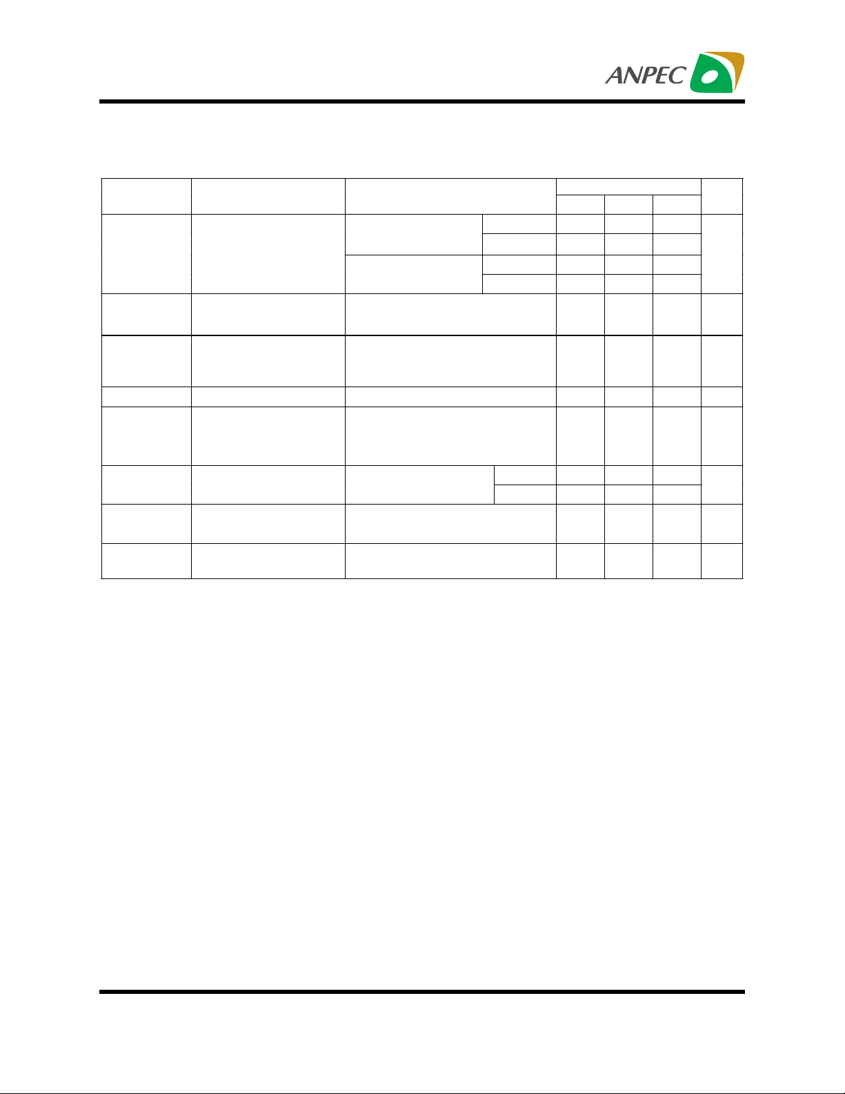
Electrical Characteristics T
= 25°C ( unless otherwise noted)
A
Symbol Parameter Test Conditions
VKA=V
V
REF
Reference voltage
T
T
A
, IK=10mA
REF
=25°C, (Fig. 1) APL431LB
A
=full range(see
Note1), (Fig.1)
V
DEF
/ ∆V
V
∆
REF
V
Temp Deviation TA =full range (see Note1)
DEF
Ratio of Change in V
to Change in Cathods
KA
, IK=10mA (Fig. 1)
REF
V
KA=VREF
IK=10mA, VKA=16V to V
Votag e
I
REF
I
REF(DEV)
Reference Input Current
I
Tem p D e vi a ti o n
REF
I
=10mA,R1 =10kΩ,R2 =∞ (Fig. 2)
K
=full range (see Note 1),
T
K
=10kΩ, R2=
R
1
,
IK=10mA,
∞
(Fig. 2)
I
K(off)
Z
I
K(MIN)
KA
off-state cathode current V
Dynamic Output
Impedance
Minimum Operating
Current
=0V, (Fig. 3)
REF
V
KA=VREF
, IK=1mA to 100mA,
f ≤1kHz (Fig. 1)
V
KA=VREF
(Fig. 1) 80 100
APL431L
Min. Typ. Max.
APL431LA 1.234 1.240 1.246
1.228 1.240 1.252
APL431LA 1.222 1.240 1.258
APL431LB 1.215 1.240 1.265
515
(Fig. 2) -0.2 -1.0 mV/V
REF
0.15 0.5
0.05 0.3
VK=6V 0.01 0.1
=16V 0.01 0.5
V
K
0.1 0.4
Unit
V
mV
A
µ
A
µ
A
µ
Ω
A
µ
Notes : 1.Full temperature range is 0°C to 70°C for APL431LXXC,and -40°C to 85°C for APL431LXXl.
Copyright ANPEC Electronics Corp.
Rev. B.7 - May., 2003
www.anpec.com.tw3

APL431L
Test figures
IN
V
REF
V
o
V
K
I
V
IN
I
K(off)
V
o
Figure 1. Test Circuit for VKA=V
V
IN
R1
R2
I
REF
REF
V
Figure 2. Test Circuit for VKA>V
VO= VKA= V
× (1+R1/R2) + I
REF
, VO=VKA=V
REF
I
K
,
REF
REF
V
o
× R
REF
1
Figure 3. Test Circuit for I
K(off)
Copyright ANPEC Electronics Corp.
Rev. B.7 - May., 2003
www.anpec.com.tw4

APL431L
Application Schematic
Precision Voltage Reference
IN
V
Precision High-Current Series Regulator
V
IN
B
R
1
R
REF
V
2
R
0.1µ F
o
V
V
o
R
Notes for Application Circuits:
B
0.1µF
R
1
V
REF
R
2
1)To improve the stability of output voltage, a 0.1µF capacitor between cathode and anode of APL431L is
strongly recommended.
2)Set VOUT according to the following equation:
VOUT = VREF(1+R1/R2)+lREF R1
3)Choose the value for RB as follows:
A)The maximum limit for RB should be such that the cathode current(lK) is greater than the minimum op erating current (80µA) at VIN(MIN).
B)The minimum limit for RB should be such that the cathode current (lK) does not exceed 100mA under
all load conditions, and the instantaneous turn-on value for lk does not exceed 150mA. Both of the fo llowing conditions must. be met:
VIN(MAX)
RB,Min≥
150mA
VIN(MAX)-VOUT
RB,Min≥
lOUT(MIN)+100mA
(to limit instantaneous turn-on lK)
(to limit lK under normal operating conditions)
Copyright ANPEC Electronics Corp.
Rev. B.7 - May., 2003
www.anpec.com.tw5

APL431L
Typical Characteristics
Cathode Current vs. Cathode Voltage Cathode Current vs. Cathode Voltage
250
VKA=V
200
150
100
50
0
-50
-100
Cathode Current (µA)
-150
-200
-250
-1-0.500.5 11.5
REF
TA=25°C
Cathode Voltage (V)
Referemce Voltage vs.
Junction Temperature
1.26
IKA=10mA
1.25
100
VKA=V
REF
TA=25°C
50
0
-50
Cathode Current (mA)
-100
-1.5 -1 -0.5 0 0.5 1 1.5
Cathode Voltage (V)
Reference Input Current vs.
Junction Temperature
0.18
IKA=10mA
R1=10kΩ, R2=∞
0.16
1.24
1.23
Reference Voltage (V)
1.22
-50 -25 0 25 50 75 100 125 150
Junction Temperature (°C)
Copyright ANPEC Electronics Corp.
Rev. B.7 - May., 2003
0.14
0.12
0.10
Reference Input Current (µA)
0.08
-50-25 0 255075100125150
Junction Temperature (°C)
www.anpec.com.tw6

APL431L
Typical Characteristics
∆V
/∆VKA vs. Junction Temperature
REF
0
-0.1
-0.2
-0.3
-0.4
-0.5
-0.6
-0.7
-0.8
-0.9
Delta Cathode Voltage (-mV/V)
-1
Ratio of Delta Reference Voltage to
-50 -25 0 25 50 75 100 125 150
IKA=10mA
∆V
KA=VREF
Junction Temperature (°C)
to 20V
Off State Cathode Current vs.
Junction Temperature
0.5
V
=0V
REF
0.4
0.3
0.2
0.1
V
=16V
KA
V
=6V
KA
Off State Cathode Current (µA)
0
-50 -25 0 25 50 75 100 125 150
Junction Temperature (°C)
3V
Input
0
1V
0
µ
0S
Output
Copyright ANPEC Electronics Corp.
Rev. B.7 - May., 2003
µ
5S
I
=1mA
KA
TA =25°C
3V
1V
I
=0.1mA
KA
TA =25°C
Input
0
Output
0
µ
0S
µ
5S
www.anpec.com.tw7

APL431L
Typical Characteristics
Gain vs. Phase Shift vs. Frequency
60
IKA=10mA
50
40
30
20
Gain (dB)
10
0
-10
10 100 1000 10000 100000 1000000
TA =25°C
Frequency (Hz)
Stability Boundary Conditions
100
90
80
70
60
50
Ik (mA)
40
30
20
10
0
0.0001 0.001 0.01 0.1 1
Unstable
V
KA =VREF
V
KA
V
KA
Stable
TA =25°C
=2.5V
=3.3V
0
50
100
150
200
250
Phase Shift (degree)
300
350
Zka (Ω)
Zka vs. Frequency
100
IKA=10mA
VKA=V
REF
TA =25°C
10
1
0.1
0.01
10 100 1000 10000 100000 1000000
Frequency (Hz)
Load Capacitance (µF)
Copyright ANPEC Electronics Corp.
Rev. B.7 - May., 2003
www.anpec.com.tw8

APL431L
Package Information
SOT-23
D
B
1
S
e
3
E H
2
A
Dim
A1
L
Millimeters Inches
Min. Max. Min. Max.
C
A 1.00 1.30 0.039 0.051
A1 0.00 0.10 0.000 0.004
B 0.35 0.51 0.014 0.020
C 0.10 0.25 0.004 0.010
D 2.70 3.10 0.106 0.122
E 1.40 1.80 0.055 0.071
e 1.90 BSC 0.075 BSC
H 2.40 3.00 0.094 0.118
L 0.37 0.0015
Copyright ANPEC Electronics Corp.
Rev. B.7 - May., 2003
www.anpec.com.tw9

APL431L
Package Information
SOT-23-5
e1
45
12
3
E1 E
e
D
Dim
Min. Max. Min. Max.
A 0.95 1.45
A1 0.05 0.15
A2 0.90 1.30
D2.83.00
E2.63.00
E1 1.5 1.70
L 0.35 0.55
b
A2
A1 L 2
A
L
a
Millimeters Inches
0.037 0.057
0.002 0.006
0.035 0.051
0.110 0.118
0.102 0.118
0.059 0.067
0.014 0.022
L 1
L1 0.20 BSC 0.008 BSC
L2 0.5 0.7
0.020 0.028
N5 5
α
0
°
10
°
0
°
10
°
Copyright ANPEC Electronics Corp.
Rev. B.7 - May., 2003
www.anpec.com.tw10

APL431L
Package Information
TO-92
3
J
e
e1
L1
Q
A
SEATING PLANE
b2
L
b
2
1
S
E
S
Millimeters Inches
Dim
Min. Max. Min. Max.
A 4.318 5.334 0.170 0.210
φ
b2
φ
D
φ
b
0.406 0.559 0.016 0.022
0.406 0.559 0.016 0.022
4.445 5.207 0.175 0.205
E 3.175 4.191 0.125 0.165
e 2.413 2.667 0.095 0.105
e1 1.143 1.397 0.045 0.055
J 3.429 0.135
L 12.70 0.500
L1 1.27 0.050
Q2.921 0.115
S 2.032 2.667 0.080 0.105
D
Copyright ANPEC Electronics Corp.
Rev. B.7 - May., 2003
www.anpec.com.tw11

APL431L
Package Information
SOT-89 (Reference EIAJ ED-7500A Reg stration SC-62)
D
D1
H
L
12 3
a
E
C
Dim
B1
B
e
e1
A
a
Millimeters Inches
Min. Max. Min. Max.
A 1.40 1.60 0.055 0.063
B 0.40 0.56 0.016 0.022
B1 0.35 0.48 0.014 0.019
C 0.35 0.44 0.014 0.017
D 4.40 4.60 0.173 0.181
D1 1.35 1.83 0.053 0.072
e 1.50 BSC 0.059 BSC
e1 3.00 BSC 0.118 BSC
E 2.29 2.60 0.090 0.102
H 3.75 4.25 0.148 0.167
L 0.80 1.20 0.031 0.047
α
10
°
10
°
Copyright ANPEC Electronics Corp.
Rev. B.7 - May., 2003
www.anpec.com.tw12

APL431L
Physical Specifications
Terminal Material Solder-Plated Copper (Solder Material : 90/10 or 63/37 SnPb)
Lead Solderability Meets EIA Specification RSI86-91, ANSI/J-STD-002 Category 3.
Reflow Condition (IR/Convection or VPR Reflow)
Reference JEDEC Standard J-STD-020A APRIL 1999
Peak temperature
temperature
Pre-heat temperature
°
183 C
Time
Classification Reflow Profiles
Convection or IR/
Convection
Average ramp-up rate(183°C to Peak) 3°C/second max. 10 °C /second max.
Preheat temperature 125 ± 25°C)
Temperature maintained above 183°C
Time within 5°C of actual peak temperature
Peak temperature range
Ramp-down rate
Time 25°C to peak temperature
120 seconds max
60 – 150 seconds
10 –20 seconds 60 seconds
220 +5/-0°C or 235 +5/-0°C 215-219°C or 235 +5/-0°C
6 °C /second max. 10 °C /second max.
6 minutes max.
VPR
Package Reflow Conditions
pkg. thickness
and all bgas
Convection 220 +5/-0 °C Convection 235 +5/-0 °C
VPR 215-219 °C VPR 235 +5/-0 °C
IR/Convection 220 +5/-0 °C IR/Convection 235 +5/-0 °C
Copyright ANPEC Electronics Corp.
Rev. B.7 - May., 2003
2.5mm
≥≥≥≥
pkg. thickness < 2.5mm and
pkg. volume
350 mm³
≥≥≥≥
pkg. thickness < 2.5mm and pkg.
volume < 350mm³
www.anpec.com.tw13

APL431L
F
Reliability test program
Test item Method Description
SOLDERABILITY MIL-STD-883D-2003
HOLT MIL-STD-883D-1005.7
PCT JESD-22-B, A102
TST MIL-STD-883D-1011.9
ESD MIL-STD-883D-3015.7 VHBM > 2KV, VMM > 200V
Latch-Up JESD 78 10ms , Itr > 100mA
Carrier Tape & Reel Dimensions
245°C , 5 SEC
1000 Hrs Bias @ 125 °C
168 Hrs, 100 % RH , 121°C
-65°C ~ 150°C, 200 Cycles
t
E
F
W
A
Po
J
P
P1
Ao
C
D
Bo
Ko
D1
T2
B
T1
Application
A B C J T1 T2 W P E
178 ±170 ± 213.5 ± 0.15 3 ± 0.15 14 ± 2 1.3 ± 0.3
SOT-89
F D D1 Po P1 Ao Bo Ko t
5.5 ± 0.05 1.5± 0.1 1.5± 0.1 4.0 ± 0.1 2.0 ± 0.1 4.8 ± 0.1 4.5± 0.1 1.80± 0.1 0.3±0.013
Application
A B C J T1 T2 W P E
178±160 ± 1.0 12.0 2.5 ± 0.15 9.0 ± 0.5 1.4
SOT-23
F D D1 Po P1 Ao Bo Ko t
3.5 ± 0.05 1.5 +0.1
Copyright ANPEC Electronics Corp.
Rev. B.7 - May., 2003
12 + 0.3
12 - 0.1
8.0+ 0.3
- 0.3
8 ± 0.1 1.75± 0.1
4.0 1.75
0.1MIN 4.0 2.0 ± 0.05 3.1 3.0 1.3 0.2±0.03
www.anpec.com.tw14

APL431L
Application
SOT-23-5
A B C J T1 T2 W P E
178 ±172 ± 1.0 13.0 + 0.2 2.5 ± 0.15 8.4 ± 2 1.5 ± 0.3 8.0 ± 0.3 4 ± 0.1 1.75± 0.1
F D D1 Po P1 Ao Bo Ko t
3.5 ± 0.05 1.5± 0.1 1.5± 0.1 4.0 ± 0.1 2.0 ± 0.1 3.15 ± 0.1 3.2± 0.1 1.4± 0.1 0.2±0.033
Carrier Tape & Reel Dimensions
F1F2
P1
H2H2A
A
P
P2
H2H2
L
L1
T2
T
T1
D2
D1
H3
W2
H4
H
W1
H1
D
W
Application
TO-92
A D D1 D2 F1,F2 H H1 H2 H2A
3.18~12 4.0±0.2 0.36~0.53 9.0 MAX
H3 H4 L L1 P P1 P2 T T1
27.0 MAX 20.0 MAX 11.0 MAX 2.5 MIN 12.7±0.2 6.35±0.4 50.8±0.5 0.55 MAX 1.42 MAX
T2 W W1 W2
0.36~0.68 17.5~19 5.0~7.0 0.5 MAX
2.5+0.2
-0.1
16±0.5 9±0.5 0.5 MAX 0.5 MAX
(mm)
Cover Tape Dimensions
Application Carrier Width Cover Tape Width Devices Per Reel
SOT- 23
SOT-23-5
SOT- 89
TO-92
8 5.3 3000
8 5.3 3000
12 9.3 1000
17.5~19 5.0~7.0 2000
Copyright ANPEC Electronics Corp.
Rev. B.7 - May., 2003
www.anpec.com.tw15
 Loading...