

ANPEC APL431CKI-TRL, APL431CKI-TR, APL431CKI-TBL, APL431CKI-TB, APL431CKI-PBL Datasheet
...
APL431
Adjustable Precision Shunt Regulator
Features General Description
••
•
Precise Reference Voltage to 2.500V
••
••
•
Guaranteed 0.5%, 1% or 2% Reference
••
Voltage Tolerance
••
•
Sink Current Capability, 1mA to 100mA
••
••
•
Quick Turn-on
••
••
•
Adjustable Output Voltage, VO = V
••
••
• Low Operational Cathode Current, 250µA
••
to 20V
ref
Typical
••
• 0.1Ω Typical Output Impedance
••
••
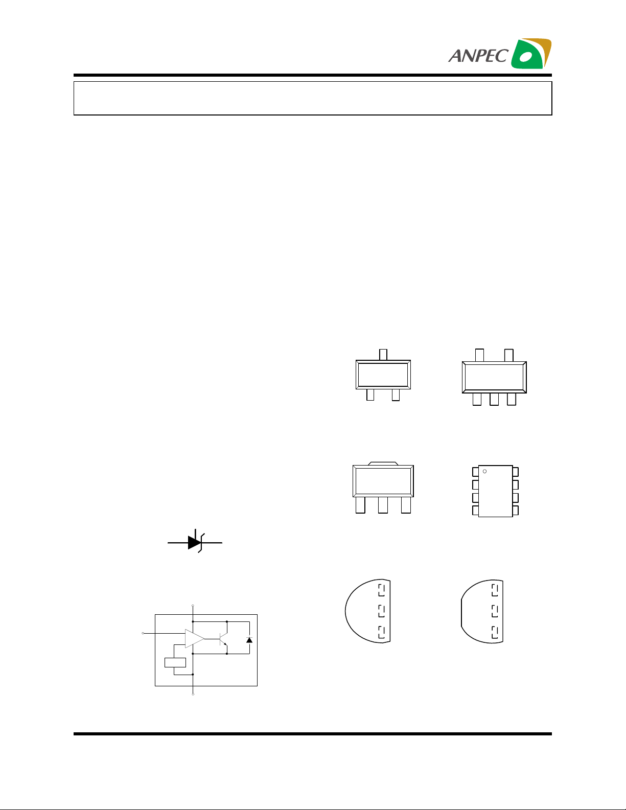
• SOT-23, SOT-23-5, SOT-89, SO-8, TO-92
••
and TO-92S Packages
Applications
••
• Linear Regulators
••
••
• Adjustable Power Supply
••
The APL431 is a 3-terminal adjustable voltage reference with specified thermal stability over applicable
commercial temperature ranges. Output voltage may
be set to any value between V
(2.5 V) and 20 V with
ref
two external resistors (see Figure 2). When used
with an photocoupler, the APL431 is an ideal voltage
reference in isolated feedback circuits for 2.5V to 12V
switching-mode power supplies. This device has a
typical output impedance of 0.1Ω. Active output circuitry provides a very sharp turn-on characteristic,
making the APL431 excellent replacements for zener diodes in many applications, including on-board
regulation and adjustable power supplies.
ANODE
3
12
REF
CATHODE
SOT-23 (Top View)
NC NC
45
123
REF ANODE
CATHODE
SOT-23-5 (Top View)
••
• Switching Power Supply
••
123
CATHODE
ANODE
ANODE
Symbol
REF
CathodeAnode
Functional Diagram
Cathode
REF
ANPEC reserves the right to make changes to improve reliability or manufacturability without notice, and advise
customers to obtain the latest version of relevant information to verify before placing orders.
Copyright ANPEC Electronics Corp.
Rev. C.1 - Jun., 2003
+
_
ref
V
Anode
REF ANODE CATHODE
SOT-89 (Top View)
CATHODE
3
ANODE
2
1
REF
TO-92 (Top View)
1
8
REF
2
7
ANODE
3
6
ANODE
4
NC
NC
5
SO-8 (Top View)
CATHODE
3
ANODE
2
1
REF
TO-92S (Top View)
www.anpec.com.tw1
APL431
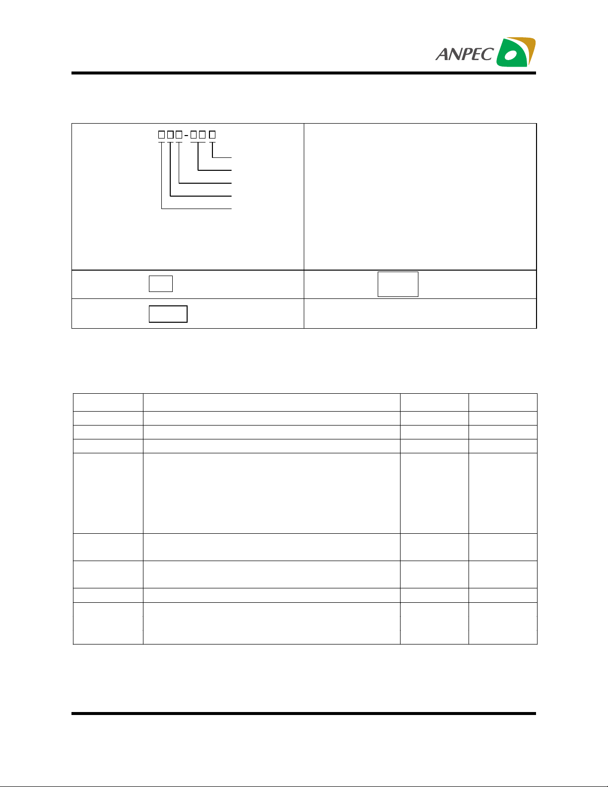
Ordering and Marking Information
APL431
APL431 A/B :
APL431 D/K :
431
APL431
XXXXX
XXXXX
Lead Free Code
Handling Code
Temp. Range
Package Code
Elec. Grade
- Date Co de
Elec. Grade
A : 0.5% Reference Voltage Tolerance
B : 1 % R efe ren ce V oltage To leranc e
C : 2 % R eferen ce V oltage To leranc e
Package C ode
A : S O T-23 B : S O T-2 3-5 D : S O T -89
E : T O -92 I : TO-92S K : SO -8
Y : C hip F orm
Temp. Range
C : 0 to 70 C I : -40 to 85 C
Handling Code
PB : P lastic Bag T B : Ta pe & B o x
TR : Ta pe & Reel
Lead Free Code
L : Lead Free Device
Blank : Orginal Device
AP L4 3 1 E /I :
°
APL
431
XXXXX
°
XXXXX - Date Code
Absolute Maximum Ratings
Symbol Parameter Rating Unit
V
KA
I
K
I
REF
θ
JA
T
A
T
j
T
STG
T
SOL
Cathode voltage
Continuous cathode current range
Reference current range
Thermal Resistance from Junction to Ambient in Free Air
SOT-23
SOT-23-5
SOT-89
TO-92
SO-8
Ambient temperature range APL431XXC
APL431XXI
Junction temperature range APL431XXC
APL431XXI
Storage Temperature Range
Lead temperature range, Ts (Soldering, 10sec)
Original Device
Lead Free Device
20 V
100 mA
3mA
416
357
250
250
210
0 to 70
-40 to 85
0 to 150
-40 to 150
-65 to 150
260
300
°C/W
°C
°C
°C
°C
Copyright ANPEC Electronics Corp.
Rev. C.1 - Jun., 2003
www.anpec.com.tw2
APL431
Electrical Characteristics (Cont.) T
Symbol Parameter Test Conditions
APL431A 2.487 2.500 2.513
,
APL431B 2.475 2.500 2.525V
1
APL431C
=10mA
1
1
REF
REF
*1
= 0V
REF
+ 50mV
*2
REF
/ T
V
∆
REF
/ ∆V
V
∆
REF
I
REF
/T
I
∆
REF
I
K(min)
I
K(off)
Reference voltage
Reference voltage
drift over temp. range
Voltage ratio (open
KA
loop gain)
Reference current
Reference current
drift
Min. cathode current VKA=V
Off-state cathode
current
|ZKA| Dynamic impedance
I
K
Cathode current VKA=V
V
KA=VREF
I
=10mA*
K
V
KA=VREF,IK
T
=0 to 70°C*
A
TA =-40 to 85°C*
IK=10mA, VKA=V
=10mA, VKA=V
I
K
I
=10mA,
K
=10kΩ, R2=open
R
1
=10mA, R1=10kΩ,
I
K
=open, TA= -40 to 85°C
R
2
REF
V
= 20V, V
KA
V
KA=VREF
IK=1mA to 100mA, f ≤1kHz
REF
= 25°C ( unless otherwise noted)
A
APL431
Min. Typ. Max.
2.450 2.500 2.550
to 10V
to 20V
*2
*2
*2
-1.5 -3
-1.2 -2.5
1.0 3
*2
0.3 1
0.25 0.5 mA
*3
*1
0.1 1
0.1 0.4
Unit
V
20
mV
30
mV/V
µ
µ
µ
Ω
100 mA
A
A
A
Notes : *1 : use Figure 1
*2 : use Figure 2
*3 : use Figure 3
Copyright ANPEC Electronics Corp.
Rev. C.1 - Jun., 2003
www.anpec.com.tw3
APL431
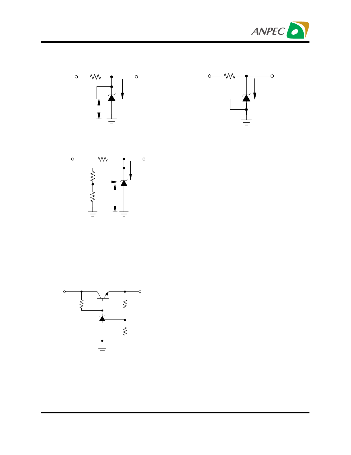
Test figures
IN
V
REF
V
Figure 1. Test Circuit for VKA=V
V
IN
R1
R2
I
REF
REF
V
Figure 2. Test Circuit for VKA>V
VO= VKA= V
× (1+R1/R2) + I
REF
K
I
, VO=VKA=V
REF
I
K
,
REF
REF
V
o
× R
V
IN
I
K(off)
REF
V
o
1
Figure 3. Test Circuit for I
K(off)
V
o
Application schematic
5-Volt Precision Regulator
V
IN
b
R
∗ R
should provide cathode current large than
b
1mA to maintain APL431 work properly.
Copyright ANPEC Electronics Corp.
Rev. C.1 - Jun., 2003
27.5k
0.1%
27.5k
0.1%
o
V
Ω
Ω
www.anpec.com.tw4
APL431
Typical Characteristics
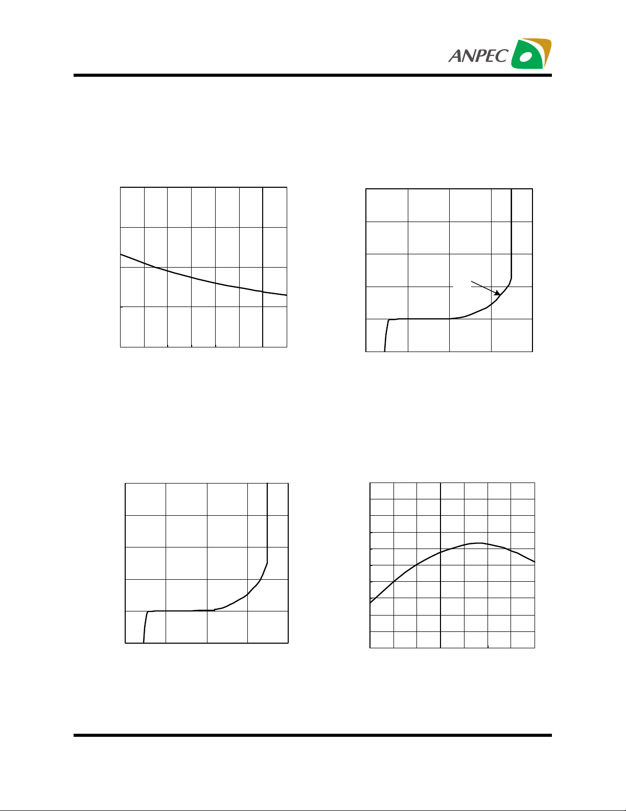
Reference Input Current vs. Temperature
2
1.5
1
0.5
Reference Input Current (µA)
0
-40-200 20406080100
Temperature (°C)
Cathode Current vs. Cathode Voltage
800
600
400
200
0
Cathode Current (mA)
-200
-1 0 1 2 3
Cathode Voltage (V)
Cathode Current vs. Cathode Voltage
800
600
400
200
Cathode Current (µA)
0
-200
-1 0 1 2 3
IK-MIN
Cathode Voltage (V)
Reference Voltage vs. Temperature
2.52
2.515
2.51
2.505
2.5
2.495
2.49
2.485
2.48
Reference Voltage (V)
2.475
2.47
-40
-20
20 40 60 80 100
0
Temperature (°C)
Copyright ANPEC Electronics Corp.
Rev. C.1 - Jun., 2003
www.anpec.com.tw5

APL431
Typical Characteristics (Cont.)
Small-Signal Voltage Amplification vs.
Frequency
60
50
40
30
20
10
0
Small-Signal Voltage Amplification (dB)
1 10 100 1000
Frequency (kHz)
Off-State Cathode Current vs. Temperature
0.5
VKA=20V
VREF=0
0.4
Pulse Response
6
Input
5
4
3
2
1
Input and Output Voltage (V)
0
345 67
Output
89
Time (µS)
Ratio of Delta Reference Voltage to
Delta Cathode Voltage vs. Tmperature
0
VKA=VREF to 20V
IK=10mA
-0.25
-0.5
10 11
12
13
0.3
0.2
0.1
Off-State Cathode Current (µA)
0
-40 -20 0 20 40 60 80 100
Temperature (°C)
Copyright ANPEC Electronics Corp.
Rev. C.1 - Jun., 2003
-0.75
-1
-1.25
-1.5
-1.75
Delta Cathode Voltage (mV/V)
Ratio of Delta Reference Voltage to
-2
-40 -20 0 20 40 60 80 100 120
Temperature (°C)
www.anpec.com.tw6

APL431
Typical Characteristics (Cont.)
Off State Cathode Current vs.
Cathode Voltage
2500
VREF=0
2000
1500
1000
500
0
Off State Cathode Current (µA)
-500
-5 0 5 10 15 20 25 30
Reference Impedance vs. Frequency
1
IK=100mA
T
A=25°C
500m
300m
200m
Reference Impedance (Ω)
100m
1k
Frequency (Hz)Cathode Voltage (V)
100k
200k2k 5k 10k 20k 50k
Stability Boundary Conditions
100
90
80
70
60
50
40
30
Cathode Current (mA)
20
10
0
0.001 0.01 0.1
VKA=VREF
VKA=3.3V
Load Capacitance (µF)
Copyright ANPEC Electronics Corp.
Rev. C.1 - Jun., 2003
TA=25°C
Stable
1
www.anpec.com.tw7

APL431
Packaging Information
SOT-23
D
B
3
1
S
e
E H
2
A
Dim
A1
L
Millimeters Inches
Min. Max. Min. Max.
C
A 1.00 1.30 0.039 0.051
A1 0.00 0.10 0.000 0.004
B 0.35 0.51 0.014 0.020
C 0.10 0.25 0.004 0.010
D 2.70 3.10 0.106 0.122
E 1.40 1.80 0.055 0.071
e 1.90 BSC 0.075 BSC
H 2.40 3.00 0.094 0.118
L 0.37 0.0015
Copyright ANPEC Electronics Corp.
Rev. C.1 - Jun., 2003
www.anpec.com.tw8

APL431
Packaging Information
SOT-23-5
e1
45
12
3
E1 E
e
D
Dim
Min. Max. Min. Max.
A 0.95 1.45
A1 0.05 0.15
A2 0.90 1.30
D2.83.00
E2.63.00
E1 1.5 1.70
L 0.35 0.55
b
A2
A
A1 L 2
a
L
Millimeters Inches
0.037 0.057
0.002 0.006
0.035 0.051
0.110 0.118
0.102 0.118
0.059 0.067
0.014 0.022
L 1
L1 0.20 BSC 0.008 BSC
L2 0.5 0.7
0.020 0.028
N5 5
α
0
°
10
°
0
°
10
°
Copyright ANPEC Electronics Corp.
Rev. C.1 - Jun., 2003
www.anpec.com.tw9

APL431
Packaging Information
SOT-89
H
L
12 3
D
D1
a
E
C
Dim
B1
B
e
e1
A
a
Millimeters Inches
Min. Max. Min. Max.
A 1.40 1.60 0.055 0.063
B 0.40 0.56 0.016 0.022
B1 0.35 0.48 0.014 0.019
C 0.35 0.44 0.014 0.017
D 4.40 4.60 0.173 0.181
D1 1.35 1.83 0.053 0.072
e 1.50 BSC 0.059 BSC
e1 3.00 BSC 0.118 BSC
E 2.29 2.60 0.090 0.102
H 3.75 4.25 0.148 0.167
L 0.80 1.20 0.031 0.047
α
10
°
10
°
Copyright ANPEC Electronics Corp.
Rev. C.1 - Jun., 2003
www.anpec.com.tw10

APL431
Packaging Information
TO-92
3
J
e
e1
L1
Q
A
SEATING PLANE
b2
L
b
2
1
S
E
S
Millimeters Inches
Dim
Min. Max. Min. Max.
A 4.318 5.334 0.170 0.210
b
φ
b2
φ
D
φ
0.406 0.559 0.016 0.022
0.406 0.559 0.016 0.022
4.445 5.207 0.175 0.205
E 3.175 4.191 0.125 0.165
e 2.413 2.667 0.095 0.105
e1 1.143 1.397 0.045 0.055
J 3.429 0.135
L 12.70 0.500
L1 1.27 0.050
Q 2.921 0.115
S 2.032 2.667 0.080 0.105
D
Copyright ANPEC Electronics Corp.
Rev. C.1 - Jun., 2003
www.anpec.com.tw11

APL431
Packaging Information
SO-8
HE
0.015X45
e1 e2
D
A1
A
1
L
0.004max.
Dim
A 1.35 1.75 0.053 0.069
A1 0.10 0.25 0.004 0.010
D 4.80 5.00 0.189 0.197
E 3.80 4.00 0.150 0.157
H 5.80 6.20 0.228 0.244
L 0.40 1.27 0.016 0.050
e1 0.33 0.51 0.013 0.020
e2 1.27BSC 0.50BSC
18
φ
Millimeters Inches
Min. Max. Min. Max.
°
8
°
Copyright ANPEC Electronics Corp.
Rev. C.1 - Jun., 2003
www.anpec.com.tw12

APL431
Physical Specifications
Terminal Material Solder-Plated Copper (Solder Material : 90/10 or 63/37 SnPb)
Lead Solderability Meets EIA Specification RSI86-91, ANSI/J-STD-002 Category 3.
Reflow Condition (IR/Convection or VPR Reflow)
Reference JEDEC Standard J-STD-020A APRIL 1999
Peak temperature
temperature
Pre-heat temperature
°
183 C
Time
Classification Reflow Profiles
Convection or IR/
Convection
Average ramp-up rate(183°C to Peak) 3°C/second max. 10 °C /second max.
Preheat temperature 125 ± 25°C)
Temperature maintained above 183°C
Time within 5°C of actual peak temperature
Peak temperature range
Ramp-down rate
Time 25°C to peak temperature
120 seconds max
60 – 150 seconds
10 –20 seconds 60 seconds
220 +5/-0°C or 235 +5/-0°C 215-219°C or 235 +5/-0°C
6 °C /second max. 10 °C /second max.
6 minutes max.
VPR
Package Reflow Conditions
pkg. thickness
and all bgas
Convection 220 +5/-0 °C Convection 235 +5/-0 °C
VPR 215-219 °C VPR 235 +5/-0 °C
IR/Convection 220 +5/-0 °C IR/Convection 235 +5/-0 °C
Copyright ANPEC Electronics Corp.
Rev. C.1 - Jun., 2003
2.5mm
≥≥≥≥
pkg. thickness < 2.5mm and
pkg. volume
350 mm³
≥≥≥≥
pkg. thickness < 2.5mm and pkg.
volume < 350mm³
www.anpec.com.tw13

APL431
F
Reliability test program
Test item Method Description
SOLDERABILITY MIL-STD-883D-2003
HOLT MIL-STD-883D-1005.7
PCT JESD-22-B, A102
TST MIL-STD-883D-1011.9
ESD MIL-STD-883D-3015.7 VHBM > 2KV, VMM > 200V
Latch-Up JESD 78 10ms , Itr > 100mA
245°C , 5 SEC
1000 Hrs Bias @ 125 °C
168 Hrs, 100 % RH , 121°C
-65°C ~ 150°C, 200 Cycles
Carrier Tape & Reel Dimensions
E
F
W
Po
A
P
P1
Ao
J
C
t
D
Bo
D1
T2
B
T1
Ko
Application
SOP- 8
A B C J T1 T2 W P E
330 ± 1 62 +1.5
12.75+
0.15
2 ± 0.5 12.4 ± 0.2 2 ± 0.2 12± 0. 3 8± 0.1 1.75±0.1
F D D1 Po P1 Ao Bo Ko t
5.5± 1 1.55 +0.1 1.55+ 0.25 4.0 ± 0.1 2.0 ± 0.1 6.4 ± 0.1 5.2± 0. 1 2.1± 0.1 0.3±0.013
Application
SOT-23
A B C J T1 T2 W P E
178±1 60 ± 1.0 12.0 2.5 ± 0.15 9.0 ± 0.5 1.4
8.0+ 0.3
- 0.3
4.0 1.75
F D D1 Po P1 Ao Bo Ko t
3.5 ± 0.05 1.5 +0.1
0.1MIN 4.0 2.0 ± 0.05 3.1 3.0 1.3 0.2±0.03
(mm)
Copyright ANPEC Electronics Corp.
Rev. C.1 - Jun., 2003
www.anpec.com.tw14

APL431
Application
A B C J T1 T2 W P E
178 ±1 72 ± 1.0 13.0 + 0.2 2.5 ± 0.15 8.4 ± 2 1.5 ± 0.3 8.0 ± 0.3 4 ± 0.1 1.75± 0.1
SOT-23-5
F D D1 Po P1 Ao Bo Ko t
3.5 ± 0.05 1.5± 0.1 1.5± 0.1 4.0 ± 0.1 2.0 ± 0.1 3.15 ± 0.1 3.2± 0.1 1.4± 0.1 0.2±0.033
Application
SOT-89
A B C J T1 T2 W P E
178 ±1 70 ± 2 13.5 ± 0.15 3 ± 0.15 14 ± 2 1.3 ± 0.3
12 + 0.3
12 - 0.1
8 ± 0.1 1.75± 0.1
F D D1 Po P1 Ao Bo Ko t
5.5 ± 0.05 1.5± 0.1 1.5± 0.1 4.0 ± 0.1 2.0 ± 0.1 4.8 ± 0.1 4.5± 0.1 1.80± 0.1 0.3±0.013
(mm)
Carrier Tape & Reel Dimensions
H2H2
L
L1
T2
T
T1
H2H2A
F1F2
P1
P
D2
A0
M
H3
W2
H4
H
W1
H1
D
D1
P2
W
40
Application
C2
C1
B2
B1
C0
A3
A2
A1
B0
T3
T4
205
UNIT : mm
A0 A1 A2 A3 B0 B1 B2 C0 C1
Box
Dimensions
330
3.18~12 90±1 76±1 30±1 90±1 31±1 76±1 5.8 3.8
C2 D D1 D2 F1=F2 F1-F2 M H H1
2.5+0.2
-0.1
±0.3 2.5±0.5 16±0.5 9±0.5
TO-92
7.8 4.0±0.2 0.36~0.53 9.0 MAX
H2 H2A H3 H4 H5=H0+M L L1 P P1
0.5 MAX 0.5 MAX 27.0 MAX 20.0 MAX 18.5±0.5 11.0 MAX 2.5 MIN 12.7±0.3 6.35±0.4
P2 T T1 T2 T3 T4 W W1 W2
50.8±0.5 0.55 MAX 1.42 MAX 0.36~0.68 15 1.7 18.0±0.2 6.0±0.2
1
≤
(mm)
Copyright ANPEC Electronics Corp.
Rev. C.1 - Jun., 2003
www.anpec.com.tw15

APL431
Cover Tape Dimensions
Application Carrier Width Cover Tape Width Devices Per Reel
SOP- 8
SOT- 23
SOT- 23-5
SOT- 89
TO-92
Customer Service
Anpec Electronics Corp.
Head Office :
5F, No. 2 Li-Hsin Road, SBIP,
Hsin-Chu, Taiwan, R.O.C.
Tel : 886-3-5642000
Fax : 886-3-5642050
Taipei Branch :
7F, No. 137, Lane 235, Pac Chiao Rd.,
Hsin Tien City, Taipei Hsien, Taiwan, R. O. C.
Tel : 886-2-89191368
Fax : 886-2-89191369
12 9.3 2500
8 5.3 3000
8 5.3 3000
12 9.3 1000
17.5~19 5.0~7.0 2000
Copyright ANPEC Electronics Corp.
Rev. C.1 - Jun., 2003
www.anpec.com.tw16
 Loading...