

Datasheet APL1087R-EC-TU, APL1087R-EC-TR, APL1087R-DC-TU, APL1087R-DC-TR, APL1087R-33EC-TU Datasheet (ANPEC)
...Page 1
APL1087R
800mA Low Dropout Fast Response Positive Adjustable Regulator and Fixed
1.8V, 2.5V and 3.3V
Features General Description
••
•
Guaranteed Output Voltage Accuracy within 2%
••
••
•
Fast Transient Response
••
••
•
Guaranteed Dropout Voltage at Multiple Cur-
••
rents
••
•
Load Regulation : 0.6% Typ.
••
••
•
Line Regulation : 0.03% Typ.
••
••
• Low Dropout Voltage : 1.3V Typ. at I
••
••
• Current Limit : 0.8A Min. at T
••
••
• On-Chip Thermal Limiting : 150 °C Typ.
••
••
• Adjustable Output : 1.25~7.15V
••
••
• Standard 3-pin SOT-89 and TO-92 Power
••
Packages.
=125°C
J
=500mA
OUT
Applications
••
• Voltage Regulator for CD-ROM Drivers
••
••
• Voltage Regulator for LAN Cards
••
The APL1087R is a low dropout three-terminal adjustable regulators with 0.8A output current capability.
In order to obtain lower dropout voltage and faster
transient response, which is critical for low voltage
applications , the APL1087R has been optimized.
The device is available in an adjustable version and
fixed output voltages of 1.8V, 2.5V and 3.3V, the output available voltage range is from 1.25~7.15V with
an input supply below 9V. Dropout voltage is guaranteed at a maximum of 1.45V at 0.5A.
Current limit is trimmed to ensure specified output
current and controlled short-circuit current. On-chip
thermal limiting provides protection against any combination of overload that would create excessive junction temperatures.
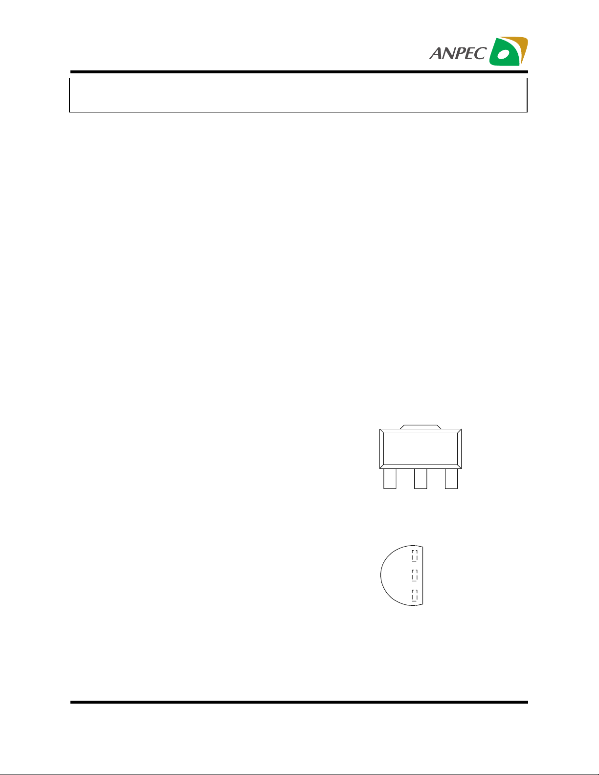
The APL1087R is available in the industry standard
3-pin SOT-89 and TO-92 power packages.
Pin Description
IN
V
APL1087R
••
• Voltage Regulator for mother Boards
••
••
• Wireless Communication Systems
••
••
• Portable Instrument
••
••
• Portable Consumer Equipment
••
••
• Low Voltage Systems
••
ANPEC reserves the right to make changes to improve reliability or manufacturability without notice, and advise
customers to obtain the latest version of relevant information to verify before placing orders.
Copyright ANPEC Electronics Corp.
Rev. A.2 - Apr., 2003
ADJ/GND
SOT-89 (Front View)
TO-92 (Top View)
213
OUT
IN
V
V
V
OUT
V
IN
ADJ/GND
www.anpec.com.tw1
Page 2
APL1087R
%
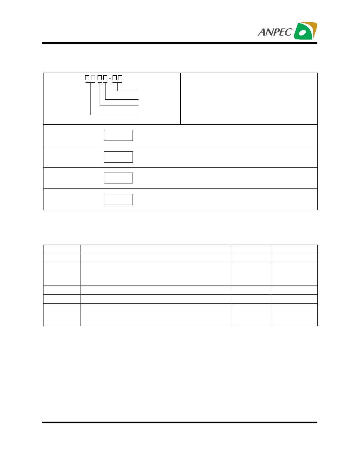
Ordering and Marking Information
APL1087R-
Handling Code
Temp. Range
Package Code
Voltage Code
APL1087R D/E :
APL1087R -25D/E :
APL1087R -33D/E :
APL1087R
XXXXX
APL1087R
XXXXX18
APL1087R
XXXXX25
APL1087R
XXXXX33
Absolute Maximum Ratings
Package Code
D : SOT-8 9 E : T O -92
Temp. Range
C : 0 to 70 C
Handling Code
TU : T ube TR : T ape & Reel
Voltage Code
18 : 1.8V 25 : 2.5V 33 : 3.3V
Blank : Adjustable Version
XXXXX - Date Code
XXXXX - Date CodeAPL1087R -18D/E :
XXXXX - Date Code
XXXXX - Date Code
°
Symbol Parameter Rating Unit
V
I
T
J
T
STG
T
L
θ
JA
Input Voltage 9 V
Operating Junction Temperature Range
Control Section
Power Transistor
0 to 125
0 to 150
Storage Temperature Range -65 to +150
Lead Temperature (Soldering, 10 second) 260
°
°
°
Thermal Resistance from Junction to Ambient in Free Air
SOT-89
TO-92
180
180
C/W
°
C
C
C
Copyright ANPEC Electronics Corp.
Rev. A.2 - Apr., 2003
www.anpec.com.tw2
Page 3
APL1087R
Electrical Characteristics
Symbol Parameter Test Conditions
REF
Reference
Voltage
V
Output Voltage
APL1087R-18
V
OUT
APL1087R-25
APL1087R-33
Line Regulation
APL1087R
REG
LINE
APL1087R-18
APL1087R-25
APL1087R-33
Load Regulation
APL1087R
REG
LOAD
APL1087R-18
APL1087R-25
APL1087R-33
V
Dropout Voltage
D
I
LIMIT
I
∆
Current Limit
Adjust Pin Current
ADJ
Adjust Pin Current
I
ADJ
Change
Minimum Load
I
O
Current
PSRR Ripple Rejection
Thermal
T
R
Regulation
Temperature
T
S
Stability
Long -Term
L
S
Stability
RMS Output
V
N
Noise
OT
Over Temperature
Point
Quiescent Current
APL1087R-18
APL1087R-25
APL1087R-33
10mA≤ I
T
=0~125°C
J
T
=0~125°C,
J
0≤ I
OUT
T
=0~125°C,
J
0≤ I
OUT
=0~125°C,
T
J
0≤ I
OUT
=0~125°C
T
J
I
10mA, 3.1V≤V
=
OUT
0mA, 3.25V≤V
I
=
OUT
I
0A, 3.95V≤V
=
OUT
0A, 4.75V≤V
I
=
OUT
T
=0~125°C
J
(V
IN –VOUT
V
=3.25V, 0≤ I
IN
=3.95V, 0≤ I
V
IN
=4.75V, 0≤ I
V
IN
I
=0.5A ,T
OUT
(V
IN -VOUT
(V
IN -VOUT
T
0~125°C, 10mA≤ I
=
J
1.45V≤V
T
=0~125°C, V
J
F
RIPPLE
(V
IN -VOUT
T
=25°C, 30ms Pulse
J
=125°C,1000Hrs.
T
J
T
=25°C,10Hz≤F≤10kHz, (% of V
J
=0~125°C,
T
J
9V
V
≤
IN
V
9V
≤
IN
9V
V
≤
IN
0.5A, 3.1V≤V
≤
OUT
0.5A, 3.25V≤V
≤
0.5A, 3.95V≤V
≤
0.5A, 4.75V≤V
≤
IN
IN
≤
IN
≤
IN
)=3V, 0≤ I
J
OUT
0.5A ,(note 1)
≤
OUT
0.5A ,(note 1)
≤
OUT
0.5A ,(note 1)
≤
OUT
=0~125°C
)=5V, TJ=25°C
=3V, I
)
IN -VOUT
=120Hz, V
=3V, TJ=0~125°C
)
=10mA, TJ=0~125°C
OUT
7.55V
≤
=9V, (note 3)
IN
RIPPLE
≤
IN
9V,
≤
IN
9V,
≤
IN
9V,
≤
IN
9V, (note1)
≤
9V, (note1)
≤
9V, (note 1)
9V, (note 1)
0.5A ,(note 1)
≤
0.5A,
≤
OUT
=1V
P-P,
9V,
OUT
APL1087R
Min. Typ. Max.
Unit
1.225 1.250 1.275 V
1.764
2.450
3.235
1.800
2.500
3.300
1.836
2.550
3.365
0.03
1
1
1
0.4 0.6
0.2
6
6
6
V
%
mV
%
1.3 1.45 V
800 mA
60 120
0.2 5
A
µ
A
µ
1.7 mA
60 75 dB
0.01 0.02 %/ W
0.5 %
0.3 %
)
0.003 %
150
5.5
5.5
5.5
10
10
10
°
mA
C
Copyright ANPEC Electronics Corp.
Rev. A.2 - Apr., 2003
www.anpec.com.tw3
Page 4
APL1087R
Electrical Characteristics (Cont.)
Note 1: See thermal regulation specifications for changes in output voltage due to heating effects. Load line regulations are mea-
sured at a constant junction temperature by low duty cycle pulse testing.
Note 2: Dropout voltage is specified over the full output current range of the device. Dropout voltage is defined as the minimum input/
output differential measured at the specified output current. Test points and limits are also shown on the Dropout Voltage curve.
Note 3: Minimum load current is defined as the minimum output current required to maintain regulation.
Application Circuits
1.25V to 7.15V Adjustable Regulator Improving Ripple Rejection
APL1087R
V
IN
+
10µ
*
C
1
OUTIN
R2
121
R1
Ω
ADJ
F
* Needed if device is far from filter capacitors
OUT
1.250VV
×=
5V Regulator with Shutdown
APL1087R
V
IN
TTL
+
10µ
F
1k
OUTIN
ADJ
1k
+
R1
APL1087R
V
OUT
100µ
+
F
*
C
2
V
10µ
ADJ
OUTIN
R1
IN
+
F
V
OUT
150µF
*
C
3
+
R2
10µ
F
* C3 improves ripple rejection.
R2R1
XC should be approximately
equal to R1 at ripple frequency
5V
Ω
121
1%
+
100µ
365
Ω
F
1%
Copyright ANPEC Electronics Corp.
Rev. A.2 - Apr., 2003
www.anpec.com.tw4
Page 5

APL1087R
Typical Characteristics
Load Transient Response
10
V
=1.25V
OUT
5
0
-5
-10
-15
-20
-25
Output Voltage Deviation (mV)
-30
0 0.1 0.2 0.3 0.4 0.5 0.6 0.7 0.8 0.9 1
Time (µs)
Adjust Pin Current vs. Temperature
3.5
3
2.5
2
1.5
1
Output Current (A)
0.5
0
-0.5
Line Transient Response
50
40
30
20
10
0
-10
Output Voltage Deviation (mV)
-20
0 0.2 0.4 0.6 0.8 1 1.2 1.4 1.6 1.8 2
Time (µs)
Current Limit vs. Temperature
7
6
5
4
3
Input Voltage (V)
2
1
0
62
61
60
59
58
57
Adjust Pin Current (µA)
56
55
-50 0 50 100 150
Temperature (°C) Temperature(°C)
940
920
900
880
860
840
820
Current Limit (mA)
800
780
760
-50 0 50 100 150
IN=
V
5V
Copyright ANPEC Electronics Corp.
Rev. A.2 - Apr., 2003
www.anpec.com.tw5
Page 6

APL1087R
Typical Characteristics (Cont.)
Dropout Voltage vs. Temperature
1.5
1.45
1.4
1.35
1.3
1.25
1.2
1.15
Drpout Voltage (V)
1.1
1.05
1
-50 -25 0 25 50 75 100 125 150
I
OUT
=500mA
Temperature (°C)
Output Voltage vs. Temperature
2.6
2.5
2.4
2.3
2.2
2.1
2
1.9
Output Voltage (V)
1.8
1.7
1.6
-50 -25 0 25 50 75 100 125
Temperature (°C)
Reference Voltage vs. Temperature
1.255
1.25
1.245
1.24
1.235
1.23
Reference Voltage (V)
1.225
1.22
-50 -25 0 25 50 75 100 125 150
Temperature (°C)
Output Voltage vs. Temperature
3.4
3.3
3.2
3.1
Output Voltage (V)
3
-50 -25 0 25 50 75 100 125
Temperature (°C)
Copyright ANPEC Electronics Corp.
Rev. A.2 - Apr., 2003
www.anpec.com.tw6
Page 7

APL1087R
Typical Characteristics (Cont.)
Output Voltage vs. Input Voltage
3.5
3
2.5
2
1.5
1
Output Voltage (V)
0.5
0
0123456789
Input Voltage (V)
Load Regulation vs. Output Current
8
V
=1.25V
OUT
7
6
5
4
3
2
Load Regulation(mV)
1
VIN=5V
Current Limit vs. Input Voltage
940
930
920
910
900
890
880
870
860
Current Limit (mA)
850
840
830
456789
Input Voltage (V)
Dropout Voltage vs. Output Current
1.8
1.6
1.4
1.2
1
0.8
Dropout Voltage (V)
0.6
0
100 200 300 400 500 600 700 800
Output Current (mA)
Copyright ANPEC Electronics Corp.
Rev. A.2 - Apr., 2003
0.4
0 200 400 600 800
Output Current (mA)
www.anpec.com.tw7
Page 8

APL1087R
Package Information
SOT-89 (Reference EIAJ ED-7500A Reg stration SC-62)
D
D1
H
L
12 3
a
E
C
Dim
B1
B
e
e1
A
a
Millimeters Inches
Min. Max. Min. Max.
A 1.40 1.60 0.055 0.063
B 0.40 0.56 0.016 0.022
B1 0.35 0.48 0.014 0.019
C 0.35 0.44 0.014 0.017
D 4.40 4.60 0.173 0.181
D1 1.35 1.83 0.053 0.072
e 1.50 BSC 0.059 BSC
e1 3.00 BSC 0.118 BSC
E 2.29 2.60 0.090 0.102
H 3.75 4.25 0.148 0.167
L 0.80 1.20 0.031 0.047
α
10
°
10
°
Copyright ANPEC Electronics Corp.
Rev. A.2 - Apr., 2003
www.anpec.com.tw8
Page 9

APL1087R
Package Information
TO-92
3
J
e
e1
L1
Q
A
L2
SEATING PLANE
b2
L
b
2
1
S
E
S
Millimeters Inches
Dim
Min. Max. Min. Max.
A 4.58 5.33 0.170 0.210
φ b
φ b2
φ D
0.41 0.53 0.160 0.021
0.41 0.48 0.160 0.019
4.96 5.20 0.175 0.205
E 3.94 4.19 0.125 0.165
e 2.42 2.66 0.095 0.105
e1 1.15 1.39 0.045 0.055
J 3.43 0.135
L 12.70 0.500
L1 1.27 0.050
L2 6.35 0.250
Q 2.93 0.115
S 2.42 2.66 0.080 0.105
D
Copyright ANPEC Electronics Corp.
Rev. A.2 - Apr., 2003
www.anpec.com.tw9
Page 10

APL1087R
Physical Specifications
Terminal Material Solder-Plated Copper (Solder Material : 90/10 or 63/37 SnPb).
Lead Solderability Meets EIA Specification RSI86-91, ANSI/J-STD-002 Category 3.
Reflow Condition (IR/Convection or VPR Reflow)
Reference JEDEC Standard J-STD-020A APRIL 1999
Peak temperature
°
temperature
Pre-heat temperature
183 C
Time
Classification Reflow Profiles
Convection or IR/
Convection
Average ramp-up rate(183°C to Peak) 3°C/second max. 10 °C /second max.
Preheat temperature 125 ± 25°C)
Temperature maintained above 183°C
Time within 5°C of actual peak temperature
Peak temperature range
Ramp-down rate
Time 25°C to peak temperature
120 seconds max.
60 ~ 150 seconds
10 ~ 20 seconds 60 seconds
220 +5/-0°C or 235 +5/-0°C 215~ 219°C or 235 +5/-0°C
6 °C /second max. 10 °C /second max.
6 minutes max.
VPR
Package Reflow Conditions
pkg. thickness ≥≥≥≥ 2.5mm
and all bags
Convection 220 +5/-0 °C Convection 235 +5/-0 °C
VPR 215-219 °C VPR 235 +5/-0 °C
IR/Convection 220 +5/-0 °C IR/Convection 235 +5/-0 °C
pkg. thickness < 2.5mm and
pkg. volume ≥≥≥≥ 350 mm³
pkg. thickness < 2.5mm and pkg.
volume < 350mm³
Copyright ANPEC Electronics Corp.
Rev. A.2 - Apr., 2003
www.anpec.com.tw10
10
Page 11

APL1087R
Reliability test program
Test item Method Description
SOLDERABILITY MIL-STD-883D-2003
HOLT MIL-STD-883D-1005.7
PCT JESD-22-B, A102
TST MIL-STD-883D-1011.9
ESD MIL-STD-883D-3015.7 VHBM > 2KV, VMM > 200V
Latch-Up JESD 78 10ms , Itr > 100mA
Carrier Tape & Reel Dimensions
E
Po
P
P1
245°C , 5 SEC
1000 Hrs Bias @ 125 °C
168 Hrs, 100 % RH , 121°C
-65°C ~ 150°C, 200 Cycles
t
D
Application
SOT-89
Application
F
W
Ao
J
A
A B C J T1 T2 W P E
178 ±1 70 ± 2 13.5 ± 0.15 3 ± 0.15 14 ± 2 1.3 ± 0.3
F D D1 Po P1 Ao Bo Ko t
D1
C
T2
B
T1
Bo
12 + 0.3
12 - 0.1
Ko
8 ± 0.1 1.75± 0.1
SOT-89 5.5 ± 0.05 1.5± 0.1 1.5± 0.1 4.0 ± 0.1 2.0 ± 0.1 4.8 ± 0.1 4.5± 0.1 1.80± 0.1 0.3±0.013
Copyright ANPEC Electronics Corp.
Rev. A.2 - Apr., 2003
(mm)
www.anpec.com.tw11
Page 12

APL1087R
Cover Tape Dimensions
Application Carrier Width Cover Tape Width Devices Per Reel
SOT- 89
Customer Service
Anpec Electronics Corp.
Head Office :
5F, No. 2 Li-Hsin Road, SBIP,
Hsin-Chu, Taiwan, R.O.C.
Tel : 886-3-5642000
Fax : 886-3-5642050
Taipei Branch :
7F, No. 137, Lane 235, Pac Chiao Rd.,
Hsin Tien City, Taipei Hsien, Taiwan, R. O. C.
Tel : 886-2-89191368
Fax : 886-2-89191369
12 9.3 1000
Copyright ANPEC Electronics Corp.
Rev. A.2 - Apr., 2003
www.anpec.com.tw12
 Loading...