

Datasheet APL1084-ZC-TUL, APL1084-ZC-TU, APL1084-ZC-TRL, APL1084-ZC-TR, APL1084-UC-TUL Datasheet (ANPEC)
...Page 1
APL1084
5A Low Dropout Fast Response Positive Adjustable Regulator and Fixed 3.3V
Features
! Fast Transient Response
! Guaranteed Dropout Voltage at Multiple Cur-
rents
! Load Regulation :0.05% Typ.
! Line Regulation : 0.03% Typ.
! Low Dropout Voltage: 1.3V Typ. at I
! Trimmed Current Limit : 5A Typ. at T
=5A
OUT
=125 °C
J
! On-Chip Thermal Limiting : 150 °C Typ.
! Standard 3-pin TO-220, TO-252 and TO-263
Power Packages
Applications
! Pentium
! powerPC
! Low Voltage Logic Supplies
! Battery-Powered Circuitry
! Post Regulator for Switching Power Supply
TM
Processor Supplies
TM
Supplies
applications, the APL1084 has been optimized. The
output available voltage range of adjustable version
is from 1.25~5.75V with an input supply below 7V,
and the fixed 3.3V output voltage device is also
available. Current limit is trimmed to ensure specified output current and controlled short-circuit current.
On-chip thermal limiting provides protection against
any combination of overload that would create excessive junction temperatures. The APL1084 is available in both the through-hole and surface mount versions of the industry standard 3-pin TO-220,TO-252
and TO-263 power packages.
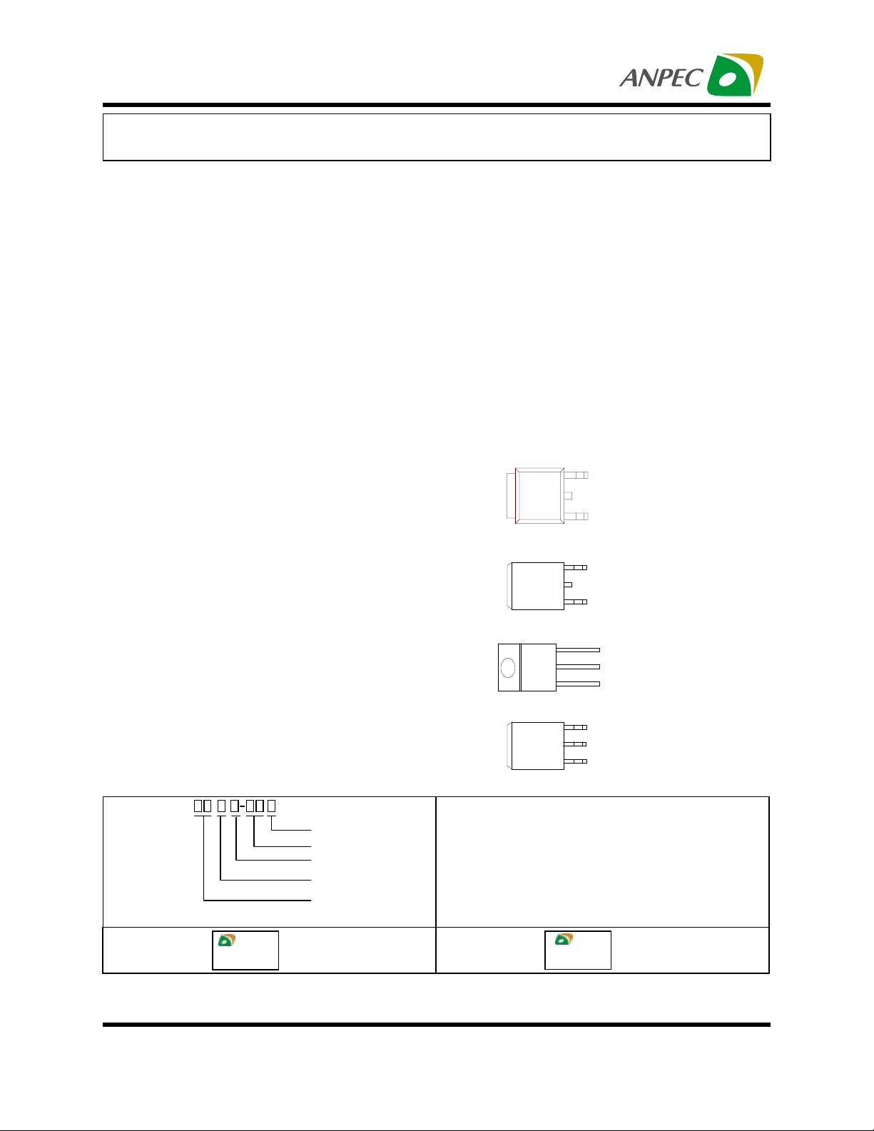
Pin Description
V
IN
Front View APL1084
V
OUT
TO-252 Package
ADJ
V
IN
Front View APL1084
V
OUT
TO-263 Package
ADJ
TAB is V
6)*EI8
OUT
OUT
!
3
2
1
General Description
The APL1084 is a low dropout three-terminal adjustable regulator with 5A output current capability. In
order to obtain lower dropout voltage and faster transient response, which is critical for low voltage
6)*E I8
6)*EI8
3
OUT
OUT
2
1
3
2
1
V
IN
V
OUT
ADJ
V
IN
Front View APL1084
V
OUT
TO-220 Package
ADJ
Front View APL1084
TO-264 Package
Ordering Information
APL1084 -
Lead Free Code
Handling Code
Tem p. Range
Package Code
Voltage Code
APL1084 :
APL1084
XXXXX
XXXXX
- Da te C od e
ANPEC reserves the right to make changes to improve reliability or manufacturability without notice, and advise
customers to obtain the latest version of relevant information to verify before placing orders.
Copyright ANPEC Electronics Corp.
Rev. B.9 - Aug., 2003
Package Code
F : T O -22 0 G : TO -263 U : TO -2 52 Z : TO -2 64
Tem p. Range
C : 0 to 70 C
Handling Code
TU : Tube TR : Tape & Reel
Voltage Code :
33 : 3.3V Blank : Adjustable Version
Lead Free Code
L : Lead Free Device Blank : Orginal Device
APL1084- 33 :
°
33
APL1084
XXXXX
XXXXX
- Da te C od e
www.anpec.com.tw1
Page 2
APL1084
Absolute Maximum Ratings
Symbol Parameter Rating Unit
V
T
T
STG
T
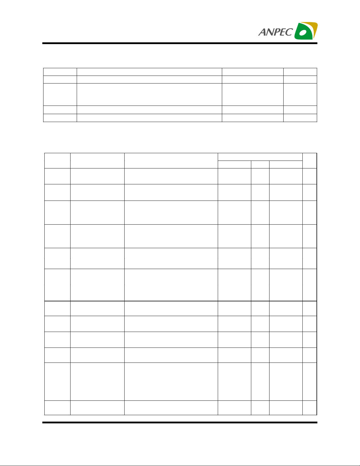
Electrical Characteristics
Input Voltage 7 V
I
Operating Junction Temperature Range
J
Control Section
Power Transistor
0 to 125
0 to 150
Storage Temperature Range -65 to +150
Lead Temperature (Soldering, 10 second) 260
L
C
°
C
°
C
°
V
Reference Voltage
REF
APL1084
V
Output Voltage
OUT
APL1084-3.3
REG
Line Regulation
LINE
APL1084
APL1084-3.3
REG
Load Regulation
LOAD
APL1084
APL1084-3.3
V
Dropout Voltage
D
I
LIMIT
I
Current Limit
Adjust Pin Current
ADJ
APL1084
Adjust Pin Current
I
∆
ADJ
Change APL1084
I
LMIN
Minimum Load
Current APL1084
I
Quiescent Current
Q
APL1084-3.3
PSRR Ripple Rejection
APL1084
APL1084-3.3
L
Long -Term
S
Stability
APL1084Symbol Parameter Test Conditions
Min. Typ. Max.
1.5V≤(V
IN -VOUT
10mA≤ I
10mA≤ I
=0~125°C
T
J
T
=0~125°C, (Notes 1)
J
2.75V≤V
4.75V≤V
T
=25°C, (Notes 1)
J
(V
IN -VOUT
V
=5V, 0mA≤ I
I N
=1% ,I
V
∆
REF
=1% ,I
V
∆
REF
(V
IN -VOUT
T
(V
IN -VOUT
T
(V
IN -VOUT
125°C
T
=0∼
J
1.5V≤( V
10mA≤ I
1.5V≤( V
T
125°C
=0∼
J
V
=5V 8 13 mA
I N
F=120Hz, C
(V
IN -VOUT
F=120Hz, C
=6.3V, I
(V
IN
T
125°C,1000Hrs.
=
J
≤5.75V,
)
=0~125°C
5A, T
≤
OUT
OUT
≤
IN
≤
IN
=3V, 10mA≤ I
)
=1.7V, T
)
=3V, T
)
=3V, I
)
IN -VOUT
≤
OUT
IN -VOUT
=3V, I
)
J
5A, 4.75V≤V
≤
7V, I
7V, I
OUT
OUT
=
OUT
=
OUT
≤
OUT
=3A ,T
=5A ,T
=10mA,
OUT
5.75V,
)
≤
10mA,
0mA ,
5A
J
J
5A
5.75V,
)
≤
=22µF, Tant. ,
out
=5A
OUT
=22µF, Tant. ,
out
=5A
OUT
OUT
=0~125°C
=0~125°C
IN
≤
5A
J
J
7V,
≤
=25°
J
125°C
=
=25°
J
125°C
=
1.225(-2%) 1.250 1.275(+2%) V
3.235(-2%) 3.300 3.365(+2%) V
0.03 0.2 %
0.05
0.05
0.3
0.5
1.2 1.4 V
1.3 1.5
C
6.0
5.0
C
6.5
5.5
7.6
6.0
8.2
6.5
60 120
0.2 5
210mA
60 dB
0.03 1.0 %
Unit
%
A
A
µ
A
µ
Copyright ANPEC Electronics Corp.
Rev. B.9 - Aug., 2003
www.anpec.com.tw2
Page 3
APL1084
Electrical Characteristics (Cont.)
APL1084Symbol Parameter Test Conditions
Unit
Min. Typ. Max.
RMS Output Noise(% of
V
θ
th,J-TAB
N
V
)
OUT
Thermal Resistance
T
C,10Hz≤F≤10kHz
=25°
J
(NOTE 2) 6.0
0.003 %
C/ W
°
Junction-to-Case, at TAB
θ
th,J-AMB
Thermal Resistance
Junction-to-Ambient
NOTE 1: See thermal regulation specifications for changes in output voltage due to heating effects. Load and line regulations are
measured at a constant junction temperature by low duty cycle pulse testing.
NOTE 2 :The value could be varied when heat sink size is different. Use larger heat sink or larger PCB size , which improves
θ
, to improve overall thermal resistance (θ
th
,TAB-A
).
th
,J-A
TO-263
TO-252
50
62.5
C/ W
°
Application Circuits
Typical Regulator
(2.75V~7V)
V
IN
10µ
C
+
F
1
APL1084
+
Solid Tantalum
C
2*
(1.250V/ 5A)
V
OUT
5V to 3.3V Regulator
V
(5V)
IN
10µ
C
1
* Required for stability
APL1084:C
* R1 is typically in range of 100Ω to 120Ω
Copyright ANPEC Electronics Corp.
Rev. B.9 - Aug., 2003
=10µF
+
F
APL1084
R2
R1
+
V
=(R1+R2)/R1*1.250V
OUT
V
(3.3V/ 5A)
OUT
Solid Tantalum
C
2*
www.anpec.com.tw3
Page 4
APL1084
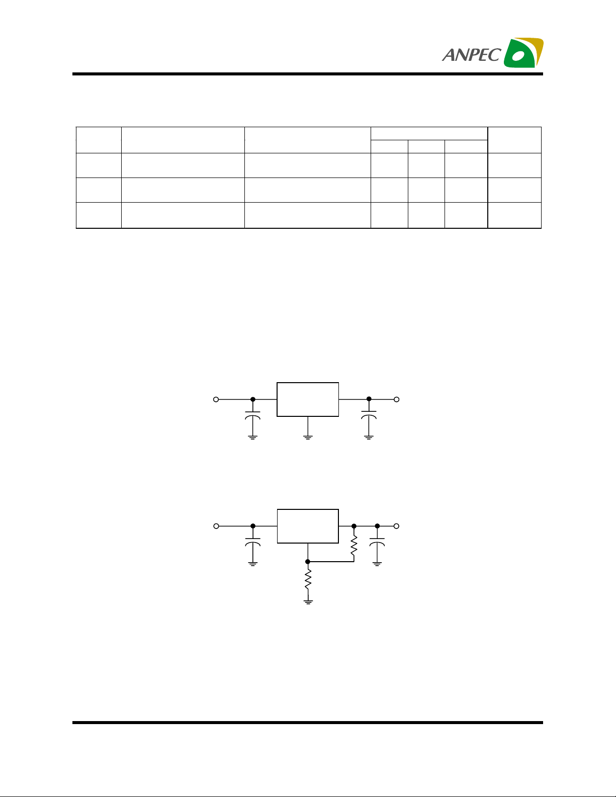
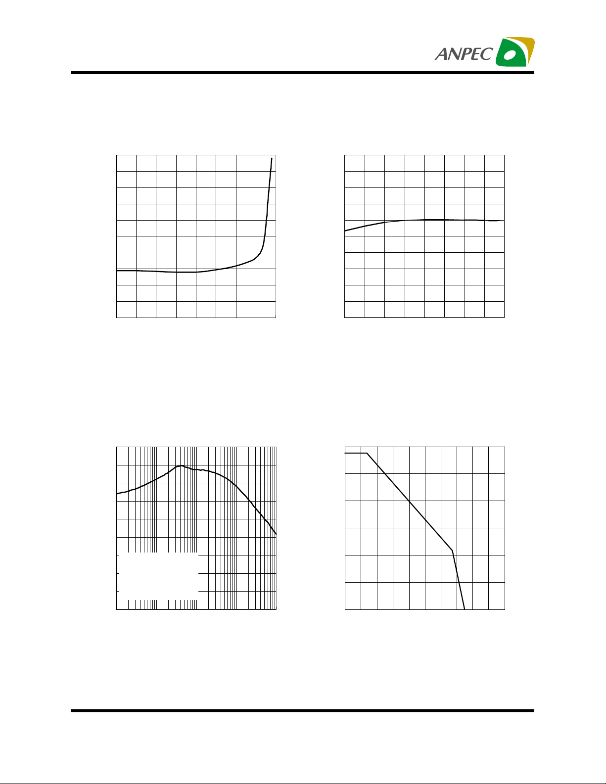
Typical Characteristics
Dropout Voltage vs Output Current
1.5
1.4
1.3
T
= -50°C
J
1.2
1.1
1.0
T
= 25°C
J
T
=125°C
J
T
J
=0°C
Dropout Voltage (V)
0.9
0.8
0.7
0.6
0.5
01 2345
Output Current (A)
Short- Circuit Current vs Temperature
16
15
14
VIN-V
OUT (SHORT CIRCUIT)
13
12
11
10
9
8
Shout- Circuit Current (A)
7
VIN-V
6
OUT(SHORT CIRCUIT)
=3.3V
-50 0 50 100 150
Temperature (°C)
=5V
Load Regulation vs Temperature
0.10
∆
I =5A
0.05
0.0
-0.05
-0.10
-0.15
Output Voltage Deviation (%)
-0.20
-50 0 50 100 150
Temperature (°C)
Reference Voltage vs Temperature
1.275
1.270
1.265
1.260
1.255
1.250
1.245
1.240
1.235
Reference Voltage (V)
1.230
1.225
-50 0 50 100 150
Temperature (°C)
Copyright ANPEC Electronics Corp.
Rev. B.9 - Aug., 2003
www.anpec.com.tw4
Page 5
APL1084
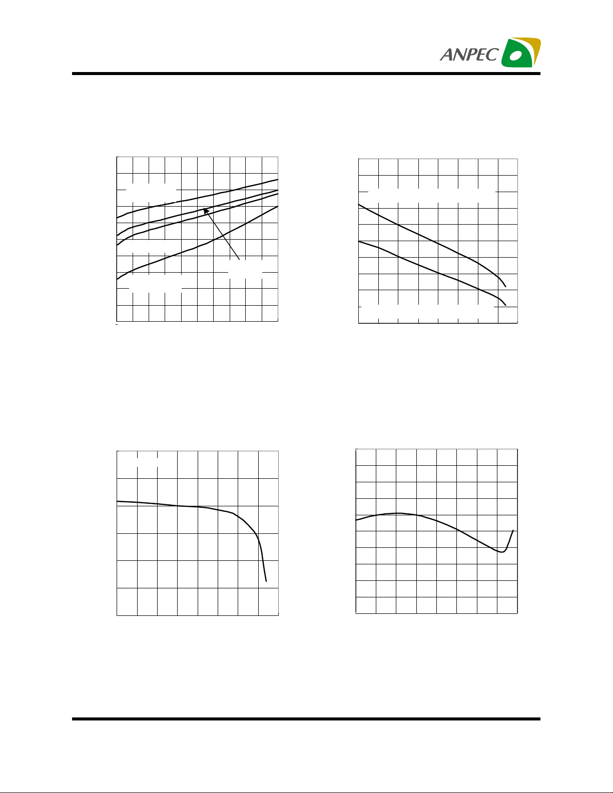
Typical Characteristics (Cont.)
Minimum Load Current vs Temperature
5
4
3
2
1
Minimum Load Current (mA)
0
-50 0 50 100 150
Temperature (°C)
Ripple Rejection vs Frequency
Adjust Pin Current vs Temperature
100
90
80
70
60
50
40
30
Adjust Pin Current (µA)
20
10
0
-50 0 50 100 150
Temperature (°C)
Maximum Power Dissipation*
90
80
70
60
50
40
30
20
Ripple Rejection (dB)
10
VIN-V
V
RIPPLE(p-p)
I
OUT
OUT
= 5A
= 3V
= 1V
0
10 100 1k 10k 100k
Frequency (Hz)
Copyright ANPEC Electronics Corp.
Rev. B.9 - Aug., 2003
!
#
#
Power (W)
#
# % '
! #
Case Temperature (°C)
* as Limited by Maximum Jcnction Temperature
www.anpec.com.tw5
Page 6

APL1084
Package Informaion
TO-252( Reference JEDEC Registration TO-252)
E
b2
L2
L1
A
C1
D
H
L
Dim
b
e1
D1
E1
Millimeters Inches
Min. Max. Min. Max.
C
A1
A 2.18 2.39 0.086 0.094
A1 0.89 1.27 0.035 0.050
b 0.508 0.89 0.020 0.035
b2 5.207 5.461 0.205 0.215
C 0.46 0.58 0.018 0.023
C1 0.46 0.58 0.018 0.023
D 5.334 6.22 0.210 0.245
D1 5.2 REF 0.205 REF
E 6.35 6.73 0.250 0.265
E1 5.3 REF 0.209 REF
e1 3.96 5.18 0.156 0.204
H 9.398 10.41 0.370 0.410
L 0.51 0.020
L1 0.64 1.02 0.025 0.040
L2 0.89 2.032 0.035 0.080
Copyright ANPEC Electronics Corp.
Rev. B.9 - Aug., 2003
www.anpec.com.tw6
Page 7
APL1084
Package Informaion
TO-263 ( Reference JEDEC Registration TO-263)
E
e
e1
A
c2
b2
b
L2
D
L
L3
Φ 1
L4
R
L1
DE TA IL "A"R O TE D
c
Millim e t e r s Inch e s
Dim
Min. Max. Min. Max.
A 4.06 4.83 0.160 0.19 0
b
0.51 1.016
0.02 0.040
b2 1.14 1.651 0.045 0.065
c 0.38 TYP. 0.015 TYP.
c2
1.14 1.40
0.045 0.055
D 8.64 9.65 0.340 0.380
e 2.54 TYP 0.100 TYP
e1
4.83 5.33
0.190 0.210
L 14.60 15.88 0.575 0.625
L1 2.24 2.84 0.090 0.110
L2
1.02 2.92
0.040 0.112
L3 1.20 1.78 0.050 0.070
Copyright ANPEC Electronics Corp.
Rev. B.9 - Aug., 2003
www.anpec.com.tw7
Page 8
APL1084
Package Information
TO-220 ( Reference JEDEC Registration TO-220)
D
Q
R
E
L1
b
e
b1
e1
H1
A
F
L
c
J1
Millim eters Inches
Dim
Min. Max. Min. Max.
A 3.56 4.83 0.14 0 0.190
b1 1.14 1.78 0.045 0.070
b 0 .51 1.14 0.020 0.0 4 5
c 0.31 1.14 0.0 1 2 0 .04 5
D 14.23 16.51 0.560 0.650
e 2 .29 2.79 0.090 0.110
e1 4.83 5.33 0.190 0.210
E 9.65 10.67 0.380 0.420
F 0.51 1 .40 0.020 0.05 5
H1 5.84 6.86 0.230 0.270
J1 2.03 2.92 0.080 0.115
L 12.7 14.7 3 0.500 0.580
L1 3.65 6.35 0.143 0.250
R 3.53 4.09 0.1 3 9 0 .16 1
Q 2.54 3.43 0.10 0 0 .13 5
Copyright ANPEC Electronics Corp.
Rev. B.9 - Aug., 2003
www.anpec.com.tw8
Page 9

APL1084
Package Information
TO-264
E
e
e1
A
b2
b
L2
D
L
c2
Φ 1
c3
DE T AIL "A"RO T ED
c
L1
Dim
A
b
b2
Min. Max. Min. Max.
4.06 4.83
0.51 1.016
1.14 1.651
c
c2
c3
D
1.14 1.40
00.102
8.64 9.65
e
e1
E
L
L1
L2
1
Φ
Copyright ANPEC Electronics Corp.
Rev. B.9 - Aug., 2003
4.83 5.33
9.65 10.54
14.60 15.88
2.24 2.84
1.02 2.92
0
°
Millimeters Inches
0.160 0.190
0.02 0.040
0.045 0.065
0.38 TYP.
0.015 TYP.
0.045 0.055
00.004
0.340 0.380
2.54 TYP
0.100 TYP
0.190 0.210
0.380 0.415
0.575 0.625
0.090 0.110
0.040 0.112
8
°
0
°
8
°
www.anpec.com.tw9
Page 10
APL1084
Physical Specifications
Terminal Material Solder-Plated Copper (Solder Material : 90/10 or 63/37 SnPb)
Lead Solderability Meets EIA Specification RSI86-91, ANSI/J-STD-002 Category 3.
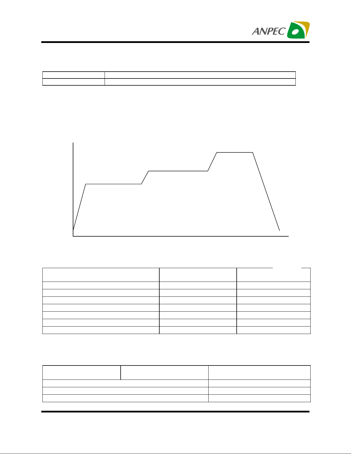
Reflow Condition (IR/Convection or VPR Reflow)
Reference JEDEC Standard J-STD-020A APRIL 1999
Peak temperature
temperature
Pre-heat temperature
°
183 C
Time
Classification Reflow Profiles
Convection or IR/
Convection
Average ramp-up rate(183°C to Peak) 3°C/second max. 10 °C /second max.
Preheat temperature 125 ± 25°C)
Temperature maintained above 183°C
Time within 5°C of actual peak temperature
Peak temperature range
Ramp-down rate
Time 25°C to peak temperature
120 seconds max
60 150 seconds
10 20 seconds 60 seconds
220 +5/-0°C or 235 +5/-0°C 215-219°C or 235 +5/-0°C
6 °C /second max. 10 °C /second max.
6 minutes max.
VPR
Package Reflow Conditions
pkg. thickness
and all bgas
Convection 220 +5/-0 °C Convection 235 +5/-0 °C
VPR 215-219 °C VPR 235 +5/-0 °C
IR/Convection 220 +5/-0 °C IR/Convection 235 +5/-0 °C
Copyright ANPEC Electronics Corp.
Rev. B.9 - Aug., 2003
2.5mm
≥≥≥≥
pkg. thickness < 2.5mm and
pkg. volume
350 mm³
≥≥≥≥
pkg. thickness < 2.5mm and pkg.
volume < 350mm³
www.anpec.com.tw10
Page 11
APL1084
R e lia bility te s t p r o g r a m
SOLDERABILITY MIL-STD-883D-2003
HOLT MIL-STD-883D-1005.7
PCT JESD-22-B, A102
TST MIL-STD-883D-1011.9
ESD MIL-STD-883D-3015.7 VHBM > 2KV, VMM > 200V
La tch-U p JE S D 78 10m s , Itr > 100m A
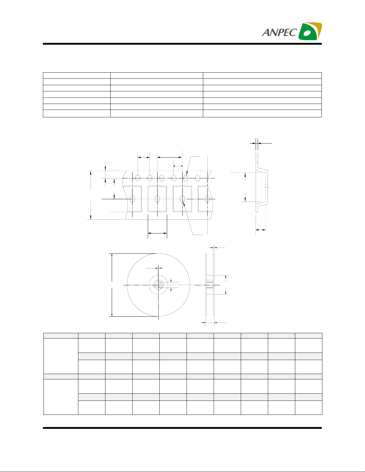
Carrier Tape
Test item Method Description
245°C , 5 SEC
1000 Hrs Bias @ 125 °C
16 8 H rs , 100 % RH , 121°C
-65°C ~ 150°C , 200 C yc les
t
E
F
W
Po
P
P1
Ao
D
Bo
Ko
D1
T2
A
Application
A B C J T1 T2 W P E
330 ±3100 ± 2 13 ± 0. 5 2 ± 0.5
TO-252
F D D1 Po P1 Ao Bo Ko t
7.5 ± 0.1 1.5 +0.1 1.5± 0.25 4.0 ± 0.1 2.0 ± 0.1 6.8 ± 0.1 10.4± 0.1 2.5± 0.1 0.3±0.05
Application
A B C J T1 T2 W P E
380±380 ± 2 13 ± 0. 5 2 ± 0.5 24 ± 4 2± 0.3
TO-263
F D D1 Po P1 Ao Bo Ko t
11.5 ± 0.1 1.5 +0.1 1.5± 0.25 4.0 ± 0.1 2.0 ± 0.1 10.8 ± 0.1 16.1± 0.1 5.2± 0.1 0.35±0.013
Copyright ANPEC Electronics Corp.
Rev. B.9 - Aug., 2003
J
C
B
T1
16.4 + 0.3
-0.2
2.5± 0.5
16+ 0.3
- 0.1
24 + 0.3
- 0.1
8 ± 0.1 1.75± 0.1
16 ± 0.1 1.75± 0.1
www.anpec.com.tw11
Page 12

APL1084
Cover Tape Dimensions
Application Carrier Width Cover Tape Width Devices Per Reel
TO- 252
TO- 263
Customer Service
Anpec Electronics Corp.
Head Office :
5F, No. 2 Li-Hsin Road, SBIP,
Hsin-Chu, Taiwan, R.O.C.
Tel : 886-3-5642000
Fax : 886-3-5642050
Taipei Branch :
7F, No. 137, Lane 235, Pac Chiao Rd.,
Hsin Tien City, Taipei Hsien, Taiwan, R. O. C.
Tel : 886-2-89191368
Fax : 886-2-89191369
16 13.3 2500
24 21.3 1000
Copyright ANPEC Electronics Corp.
Rev. B.9 - Aug., 2003
www.anpec.com.tw12
 Loading...