

Page 1
A
2
a
4
e
t
U
7
a
0
na
ren In
tegra
ed R
dio
A85
Man
Rele
0E2
ual
se Dat
A91
Dec 2
sers
th
201
Page 2

Page ii of 28 A8520E24A91 – Users Manual
Release Date: Dec 27
th
2010
THIS PAGE LEFT INTENTIONALLY BLANK
Page 3

n
O
h
r
l
C
h
e
T
F
o
r
r
e
L
U
x
n
l
a
M
n
p
n
g
m
U
.
.
.
d
H
.
.
n
qu
.
.
a
S
.
a
.
.
t
e
a
P
.
r
o
.
.
.
t
.
.
.
o
a
.
.
.
.
.
.
.
.
.
.
.
E
F
.
.
.
.
.
.
.
.
.
.
.
.
.
.
.
.
.
.
.
.
.
.
.
.
.
.
.
.
.
.
.
.
.
.
.
.
.
.
.
.
.
ii
5
6
6
9
0
3
3
3
4
4
4
5
7
8
8
9
9
2
3
4
4
5
i
Conte
1.
1.1.
2.
2.1.
2.2.
2.3.
3.
3.1.
3.2.
3.3.
4.
4.1.
4.2.
4.3.
4.4.
4.5.
5.
5.1.
5.2.
ts
verview ......
Features ...
T
eory of Op
Network
Adaptive
Applicati
P
oduct App
USA (Fed
3.
1.1.FCC
3.
1.2.End
1.3.RF E
3.
Canada (I
Potential I
E
ectrical Ch
Absolute
Operating
Pin Out ....
Recomme
Power Su
onfiguratio
Calibratin
Program
.....................
.....................
ration .........
opology an
requency
ns ................
ovals ...........
ral Commu
abeling Re
ser Manual .
osure .........
dustry Can
nterference
racteristics .
aximum R
Conditions
.....................
ded Layou
ply Consid
and Progr
Transmit
ing ..............
se
M
....................
....................
....................
Nomencla
opping .......
....................
....................
ications C
irements ......
.....................
.....................
da, IC).......
ources .......
....................
tings ..........
....................
....................
....................
rations .......
mming .......
ower ..........
....................
s M
del A8520
.....................
.....................
.....................
ure ..............
.....................
.....................
.....................
mmission,
.....................
.....................
.....................
.....................
.....................
.....................
.....................
.....................
.....................
.....................
.....................
.....................
.....................
.....................
anu
24A91
.....................
.....................
.....................
.....................
.....................
.....................
.....................
CC, ) .....
.....................
.....................
.....................
.....................
.....................
.....................
.....................
.....................
.....................
.....................
.....................
.....................
.....................
.....................
al
....................
....................
....................
....................
....................
....................
....................
....................
.....................
.....................
.....................
....................
....................
....................
....................
....................
....................
....................
....................
....................
....................
....................
.....................
.....................
.....................
.....................
.....................
.....................
.....................
.....................
.....................
.....................
.....................
.....................
.....................
.....................
.....................
.....................
.....................
.....................
.....................
.....................
.....................
.....................
....................
....................
....................
....................
.................. 1
.................. 1
.................. 1
.................. 1
.................. 1
.................. 1
.................. 1
.................. 1
.................. 1
.................. 1
.................. 1
.................. 1
.................. 1
.................. 2
.................. 2
.................. 2
.................. 2
.................. 2
Page 4

Page iv of 28 A8520E24A91 – Users Manual
Release Date: Dec 27
th
2010
THIS PAGE LEFT INTENTIONALLY BLANK
Page 5

A8520E24A91 – Users Manual Page 5 of 28
Release Date: Dec 27
th
2010
1. Overview
The A8520E24A91 series modules are surface mount modules integrating a CC85xx
PurePath™ wireless audio transceiver with the CC2591 PA/LNA device for increased range
and an integral antenna. The module incorporates a crystal, the required RF matching and
filtering for FCC compliance as well as filtering on all digital lines for noise reduction and
sensitivity. The modules operate in the global non-licensed 2.4GHz ISM/SRD frequency band.
These radio modules are ideal for achieving low power, lo ng range wireless connectivity withou t
having to deal with extensive Protocol, RF, antenna design and regulatory compliance, allowing
quick time to market. The modules are 100% tested to provide consistent performance.
The A8520E24A91 series modules have received regulatory approvals for modular devices in
the United States (FCC) and Canada (IC). The modular approval allows the end us er to place
an A8520E24A91 module inside a finished product without having to perform costly regulatory
testing for an intentional RF radiator. Section 3 has information on the requirements for the end
user/integrator must fulfill to use the modules without intentional radiator regulatory testing.
The A85xxE91A91 is based on the CC85xx series chips and the CC2591 c hip, both from Texas
Instruments. All control lines are provided at module lev el for full control of its operation. Please
see the CC85xx and CC2591 data sheet (www.ti.com) for how to o perate, program and control
the module. The PurePath™ protocol is developed, by Texas Instruments, specifically for the
CC85xx series chips and specifically for digital audio distribution. At the extremes of its range,
the protocol provides graceful degradation of the audio s ignal usign algo rithms like interpolation,
to make intermittent connectivity inaudible. Thus the A8520E24A91 series modules are not
suitable for strict data transport.
The module/protocol is configured and programmed by the OEM/Integ rator to setup the specific
Codec chip used for audio conversion and to setup control buttons and manufacturer/network
addresses. This is described in detail in the CC85xx datasheet, users guide and PurePath™
documentation on Texas Instruments web (www.ti.com
transmit power from the module is covered in section 5.1.
The A8520E24A91 module measures 11x19x2mm and are footprint compatible with other
family members:
• A85xxE24A90 – ETSI compliant version similar to the A8520E24A91.
• A85xxR24A00 – Lower power consumption, shorter range modulens.
). Specifics pertaining to calibrating the
Page 6

Page 6 of 28 A8520E24A91 – Users Manual
Release Date: Dec 27
th
2010
1.1. Features
Features:
• Un-Compressed Wireless Audio
Connectivity
• Pre-defined protocol
• Configurable human interface
• Autonomous or Hosted mode
Benefits Summary:
• Operating temperature -40 to +85C
• 100% RF Tested in production for
repeatable performance
• Common footprint for multiple fami ly
members
• No RF engineering experience
necessary
• No protocol experience necessary
• Only requires a 2 layer Host PCB
implementation
• FCC & IC certified
• No regulatory “Intentional radiator”
testing required to integrate module
into end product. Simple certi f ic at io n
labeling replaces testing.
2. Theory of Operation
The A8520E24A91 interfaces directly to a audio Codec chip through the I2S for audio data and
though I
2
C fro volume control and other Codec chip settings.
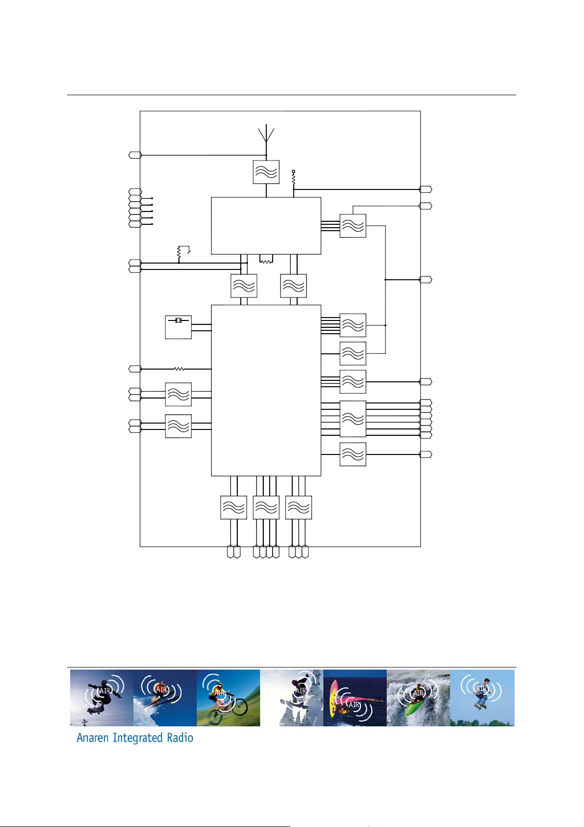
Below a block diagram is given for the A8520E24A91 module.
• Antenna
o The antenna couples energy between the air and the module. The integral
antenna provides a near omni-directional antenna pattern with high efficiency;
such that the application will work equally well in any direction. Note that the end
radiation pattern depend not only on the antenna, but also the ground plane,
enclosure and installation environment.
• Filtering
o Filtering removes spurious signals to comply with regulatory intentional radiator
requirements as well as provide reduced susceptibility to power supply and
digital noise, as well as filter out RF and high frequency noise from the digital
audio and control link (I
• Matching
o The matching provides the correct loading of the transmit amplifier to achieve the
highest output power as well as the correct loading for the receive LNA to
achieve the best sensitivity.
• Protocol
2
S, I2C).
Page 7

A8520E24A91 – Users Manual Page 7 of 28
Release Date: Dec 27
th
2010
o The protocol implements an entire wireless audio transport mechanism with
adaptive frequency usage, retransmission of lost packets as well as a low data
rate link for remote control purposes.
Page 8
Page 8 of 28 A8520E24A91 – Users Manual
Release Date: Dec 27
th
2010
DNC (RF-Test)
GND
GND
GND
GND
GND
GND
XPAEN/GIO14
XLNAEN/GIO15
VBAT
SCL
SDA
GIO12
GIO13
2
AVdd
100k
31
1
3
12
22
30
34
100k
10
11
48MHz
5
6
7
8
9
100k
CC259x
PAEN
EN
X0
X1
XPAEN/GIO14
XLNAEN/GIO15
VBAT
SCL
SDA
GIO12
GIO13
CC85xx
Bias
HGM
RF
RF
AD2/GIO9
AD1
AD0
WCLK
BCLK
MCLK
AVdd
AVdd
DVdd
IOVdd
HGM
DNC (AVdd_CC259x)
4
33
Vdd
32
IOVdd
29
AD2/GIO9
28
AD1
AD0
27
26
WCLK
25
BCLK
24
MCLK
RSTN
XANTP/USBP
XANTN/USBM
13
XANTN/USBM
SCLK
CS_N
MOSI
MISO
18
17
16
15
14
MOSI
MISO
CS_N
SCLK
XANTP/USBP
GIO3
GIO2
GIO1
21
20
19
GIO1
GIO2
GIO3
23
RSTN
Figure 1 the functionality of the A852 0E24A91, using an integral antenna
Page 9

A8520E24A91 – Users Manual Page 9 of 28
Release Date: Dec 27
th
2010
2.1. Network Topology and Nomenclature
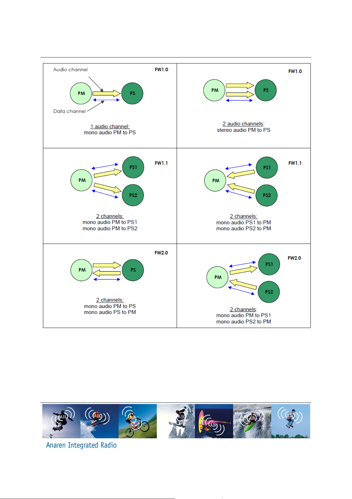
A A8520E24A91 network consists of one Protocol Master (PM) and one or two Protocol
Slave(s) (PS). The PM provides the audio reference clock and controls network association.
The PS regenerate the audio reference clock based on the packets received. Audio can be
transmitted from the PM to a PS. The device receiving the audio is called an Audio Sink, the
device sending the audio is called an Audio Source. A device can be both Audio Sink and Audio
Source at the same time (bidirectional audio will be supported in future revisions of the
firmware). The CC8520 network also includes a Data Side-Channel which is a bi-directional
data link between the PM and all PS in the network. This is further described in chapter 8.
Error! Reference source not found. Illustrates the different network topologies that can be
formed with CC8520 using the different firmware versions.
Page 10
Page 10 of 28 A8520E24A91 – Users Manual
Release Date: Dec 27
th
2010
Figure 2 A8520E24A91 topologies supported for d ifferent A8520E24A91 F W revisions
2.2. Adaptive Frequency Hopping
The purpose of using frequency hopping in a radio system is to provide diversity that allows
data throughput to be maintained even if interfering radio systems or the physical environment
(e.g. multipath fading) renders some RF channels unusable. In the 2.4 GHz ISM band, the
sheer amount of radio systems and the severity and dynamic nature of indoor fading
phenomena in typical operating environments require the use of this kind of diversity if a
Page 11

A8520E24A91 – Users Manual Page 11 of 28
Release Date: Dec 27
th
2010
minimum data throughput is to be guaranteed (as audio streaming requires). Frequency
hopping systems can either implement a fixed sequence of channel hops or adapt its hopping
sequence dynamically to the changing environment it operates in. In order to maximize its ow n
chances of delivering audio data in time and to co-exist amicably with other fixed-frequency or
adaptive frequency hopping systems, PurePath Wireless uses an adaptive frequency hopping
(AFH) scheme that adapts to changing conditions within tens of milliseconds. PurePath
Wireless divides the 2.4 GHz band into 18 RF channels with 4 MHz bandwidth. A protocol
master, which controls the adaptive frequency hopping scheme for the audio network, maintains
a table with an entry for each RF channel and an associated quality-of-service (QoS) estimate
for each. Each time an RF channel is used the QoS estimate is updated based on what
happens during the timeslot. The frequency hopping algorithm separates the 18 RF channels
into two sets:
• A set of 4 active channels
• A set of 14 trial channels
The active channel set contains the preferred RF channels that have proven that they provide
sufficiently good quality-of-service. The trial channel set contains the remaining RF channels
that are only evaluated occasionally in order to be able to maintain an accurate picture of their
quality-of-service. If the QoS estimate of an RF channel in the active set goes beyond a
minimum threshold this channel is swapped out with the RF channel in the trial chan nel set that
has the best QoS estimate. Other factors play in when selecting a new RF channel to the active
channel set, such as trying to maintain a certai n minimum distance in frequency between the
different active channels.
Page 12
Page 12 of 28 A8520E24A91 – Users Manual
Release Date: Dec 27
th
2010
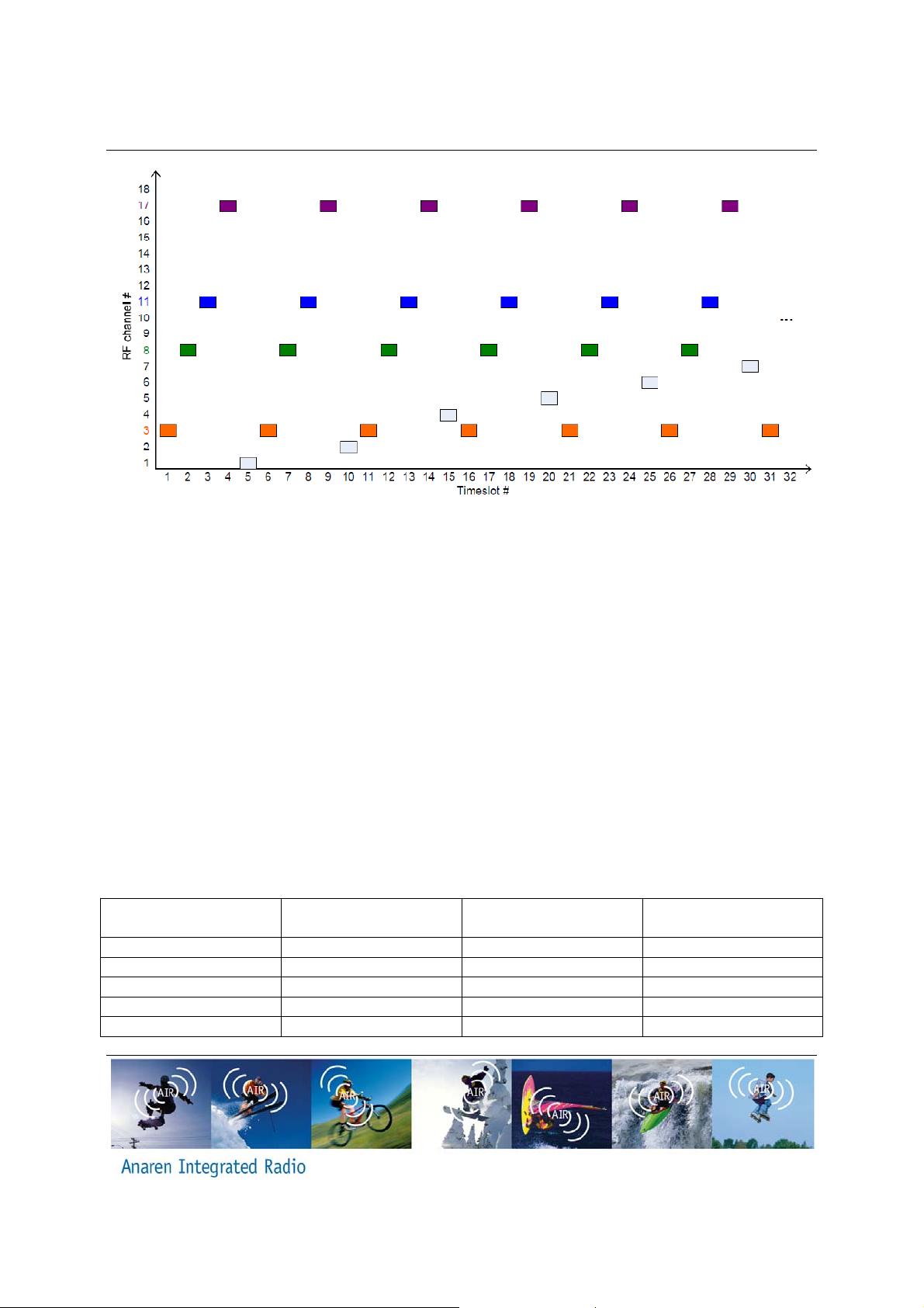
Figure 3 Example of AFH hop seq uence (ac tive se t in c olor, trial set i n black/gray)
The frequency hopping algorithm, when no swaps between the active and trial channel sets
occur, goes through a sequence of 70 hops over the course of which every RF channel has
been used.
• This 70-hop macrosequence consists of 14 repetitions of a
o 5-hop microsequence during which
Each of the four active RF channels are used once
One of the trial RF channels is used once (cycling through all trial
channels over the course of a macrosequence)
Figure 3 illustrates this concept. This gives an average steady-state RF channel usage in an
audio network of:
• Each of the four active channels are used 20% of the time
• Each trial channel is used 1.43% of the time
The channels correspond to center frequencies as follows:
Channel Center Frequency
[MHz]
Channel Center Frequency
[MHz]
1 2406 10 2442
2 2410 11 2446
3 2414 12 2450
4 2418 13 2454
5 2422 14 2458
Page 13
3
1
A8
-
a
A
E
a
a
n
a
o
A
a
o
A
A
a
p
e
e
p
t
m
d
1
o
S
1
e
a
o
d
o
s
7
6
0
4
8
o
m
s
A
h
e
g
d
C
e
c
s
y
A
F
r
c
m
e
e
d
m
s
e
:
5161718
C
a
e
m
s
e
m
A1
g
q
R
c
u
a
0
a
s
f
a
a
m
s
a
g
C
r
e
b
e
s
m
8
n
t
r
e
C
e
e
d
6
7
8
9
Release D
2.
. A
•
Wireless h
•
Wireless h
•
Wireless s
•
Wireless s
•
Wireless
8520E24
91 – User
te: Dec 2
242
243
243
243
plicati
adphones
adsets
eakers
udio equip
icrophone
Manual
th
2010
ns
ent
ge 13 of 2
P
1
2462
2466
2470
2474
3.
The A8
particul
3.
The
15 sub
approv
8520
approv
(15.19
followi
must
operati
ny ch
could v
Pro
520E24A9
ar the radi
. U
520E24A9
part C “Int
l as det
24A91 mo
ls.
3) The m
g two con
ccept any
n.
nges or m
id the use
uct
have bee
modules
A (F e d
, with inte
ntional Ra
iled in F
dule can b
dules com
itions: (1) t
interferen
dification
r’s authorit
pp
n designed
ave been
ral Co
rated ant
iators. Th
C public
integrate
plies with
his device
e receive
not expre
to operat
naren
oval
to meet F
ertified to t
munic
nna has b
devices
notice DA
into a fini
part 15 of
ay not ca
d, includin
sly approv
the equip
s
C and Ind
he followin
tions C
en tested
eet the re
00-1407
hed produ
the FCC r
use harmf
g interfere
d by the p
ent.
ustrie Can
.
ommis
to comply
uirements
eleased:
t with obt
ules. Oper
l interferen
nce that
rty respon
da (IC) re
ion, FC
with FCC
or modula
June 26,
ining subs
tion is su
ce, and (2)
ay caus
ible for co
ulations. I
C, )
FR47 Par
transmitte
2000. Th
quent FC
ject to th
this devic
undesire
pliance
CC ID
X7J-
00517
1
Page 14

Page 14 of 28 A8520E24A91 – Users Manual
Release Date: Dec 27
th
2010
3.1.1. FCC Labeling Requirements
The A8520E24A91 modules have been labeled with their own FCC ID number an d if the FCC
ID is not visible when the module is installed inside another device, then the outside of the
finished product into which the module is installed must also display a label referring to the
enclosed module. This exterior label can use wording such as the following:
Contains Transmitter Module FCC ID: X7J-A10051701
-orContains FCC ID: X7J-A10051701
This device complies with Part 15 of the FCC Rules.
Operation is subject to the following two conditions:
(1) this device may not cause harmful interference, and (2) this device must accept any
interference received, including interference that may cause undesired operation.
3.1.2. End User Manual
The end user manual should include the following statement:
This equipment has been tested and found to comply with the limits for a C lass B digital devic e,
pursuant to part 15 of the FCC Rules. These limits are designed to provide reasonable
protection against harmful interference in a residential installation. This equipment generates,
uses and can radiate radio frequency energy and, if not ins talled and used in accordance with
the instructions, may cause harmful interference to radio communications. However, there is no
guarantee that interference will not occur in a particular installation. If this equipment does
cause harmful interference to radio or television reception, which can be determined b y turning
the equipment off and on, the user is encouraged to try to correct the interference by one or
more of the following measures:
• Reorient or relocate the receiving antenna.
• Increase the separation between the equipment and receiver.
• Connect the equipment into an outlet on a circuit different from that to which the receiver
is connected.
• Consult the dealer or an experienced radio/TV technician for help.
3.1.3. RF Exposure
All transmitters regulated by FCC must comply with RF exposure requirements. OET Bulletin 65
“Evaluating Compliance with FCC Guidelines for Human Exposure to Radio Frequency
Page 15

A8520E24A91 – Users Manual Page 15 of 28
Release Date: Dec 27
th
2010
Electromagnetic Fields” provides assistance in determining whether proposed or existing
transmitting facilities, operations or devices comply with limits for human exposure to Radio
Frequency (RF) fields adopted by the Federal Communications Commission (FCC). The bulletin
offers guidelines and suggestions for evaluating compliance.
If appropriate, compliance with exposure guidelines for mobile and unlicensed de vices can be
accomplished by the use of warning labels and by providing users with information concerning
minimum separation distances from transmitting structures and proper installation of antennas.
The following statement must be included as a CAUTION statement in manuals and OEM
products to alert users of FCC RF Exposure compliance:
To satisfy FCC RF Exposure requirements for mobile and base station transmission devic es, a
separation distance of 20 cm or more should be maintained between the antenna of this device
and persons during operation. To ensure compliance, operation at closer than this distance is
not recommended. The antenna(s) used for this transmitter must no t be co-located or operating
in conjunction with any other antenna or transmitter.
If the A8520E24A91 module is used in a portable application (antenna is less than 20 cm from
persons during operation), the integrator/OEM is responsible for performing Specific Absorption
Rate (SAR) testing in accordance with FCC rules 2.1093.
3.2. Canada (Industry Canada, IC)
The A8520E24A91 modules has been certified for use in Canada under Indus try Canada (IC)
Radio Standards Specification (RSS) RSS-210 and RSS-Gen.
Host devices which contain separately certified modules do not need to be recertified, provided
that they meet the following conditions:
a) The host device, as a stand-alone unit without any separately certified modules, complies
with all applicable Radio Standards Specifications.
b) The host device and all the separately certified modules it contains jointly meet the RF
exposure compliance requirements of RSS-102, if applicable.
c) The host device complies with the certification labeling requirements of each of the modules it
contains.
Note: Compliance of a module in its final configuration is the responsibility of the applicant. A
host device will not be considered certified if the instructions regarding antenna configuration
provided in the original description, of one or more separately certified modules it contains, were
not followed.
Page 16

Page 16 of 28 A8520E24A91 – Users Manual
Release Date: Dec 27
th
2010
3.2.1. IC Labeling Requirements
From section 3.2.1 RSS-Gen, Issue 3, December 2010, Labeling Requirements for the Host
Device:
The host device shall be properly labeled to identify the modules within the host device. The
Industry Canada certification label of a module s hall be c learly visible at all times when installed
in the host device, otherwise the host device must be labeled to display the Industry Canada
certification number of the module, precede d by the words “Contains tra nsmitter module”, or the
word “Contains”, or similar wording expressing the same meaning
From section 5.2, RSS-Gen, Issue 3, December 2010, Equipment Certification Numbers and
Labels: Every unit of Category I radio apparatus certified for marketing and use in Canada shall
bear a permanent label on which is indelibly displayed the model number and Industry Canada
certification number of the equipment model (transmitter, receiver, or inseparable combination
thereof). Each model shall be identified by a unique combination of a model number and a
certification number, which are assigned as described below in this section.
The label shall be securely affixed to a permanently attached part of the device, in a location
where it is visible or easily accessible to the user, and shall not be readily detachable. The label
shall be sufficiently durable to remain fully legible and intact on the device in all normal
conditions of use throughout the device’s expected lifetime. These requirements may be met
either by a separate label or nameplate permanently attached to the device or by permanently
imprinting or impressing the label directly onto the device.
The label text shall be legible without the aid of magnification, but is not required to be larger
than 8-point font size. If the device is too small to meet this condition, the label information may
be included in the user manual upon agreement with Industry Canada.
Label:
Contains/Contient IC: 8975A- A10051701
Notice: This device complies with Industry Canada licence-exempt RSS standard(s). Operation
is subject to the following two conditions: (1) this device may not cause interference, and (2) this
device must accept any interference, including interference that may cause undesired opera tion
of the device.
Avis: Cet appareil est conforme avec Industrie Canada RSS standard exempts de licence (s).
Son fonctionnement est soumis aux deux conditions suivantes: (1) cet appareil ne peut pas
provoquer d'interférences et (2) cet appareil doit accepter toute interférence, y compris les
interférences qui peuvent causer un mauvais fonctionnement du dispositif.
For more information see: Industry Canada http://www.ic.gc.ca/
Page 17

A8520E24A91 – Users Manual Page 17 of 28
Release Date: Dec 27
th
2010
3.2.2. RF Exposure
All transmitters regulated by IC must comply with RF exposure limits as set forth in RSS-102,
Issue 4, section 4, “Exposure Limits”. Furthermore RSS-102, Issue 4, Section 2 “Certification
Requirements”, provides assistance in determining the specific requirements for compliance . If
appropriate, compliance with exposure guidelines for mobile and unlicensed devices can be
accomplished by the use of warning labels and by providing users with information concerning
minimum separation distances from transmitting structures and proper installation of antennas.
The following statement must be included as a CAUTION statement in manuals and OEM
products to alert users of IC RF Exposure compliance:
Notice: To satisfy IC RF Exposure requirements for mobile and base station transmission
devices, a separation distance of 20 cm or more should be maintained between the antenna of
this device and persons during operation. To ensure compliance, operation a t closer than this
distance is not recommended. The antenna(s) used for thi s transmitter must not be co-located
or operating in conjunction with any other antenna or transmitter.
Avis: Pour répondre à la IC d'exposition pour les besoins de base et mobiles dispositifs de
transmission de la station, sur une distance de s éparation de 20 cm ou plus doit être maintenue
entre l'antenne de cet appareil et les personnes en cours de fonc tionnement. Pour assurer le
respect, l'exploitation de plus près à cette distance n'est pas recommandée. L'antenne (s) utilisé
pour cet émetteur ne doit pas être co-localisés ou fonctionner conjointement avec une autre
antenne ou transmetteur.
If the A8520E24A91 module is used in a portable application (antenna is less than 20 cm from
persons during operation), the integrator/OEM is responsible for performing Specific Absorption
Rate (SAR) testing in accordance with IC rules and methods of RSS-102.
3.3. Potential Interference Sources
The two main mechanisms that allow a PurePath wireless system to co-exist amicably in close
proximity to other 2.4 GHz radio systems are:
• The adaptive frequency hopping scheme described in section 2.4.3 that ensures that RF
channels used by other radio systems are avoided
• Adaptive listen-before-talk mechanism that measures energy in RF channel before
transmitting and avoids transmitting if the channel is already in use
These mechanisms together ensure that other radio systems are minimally impacted by a
PurePath Wireless audio network in normal circumstances. However, since a low-latency audio
network by its very nature transports a very time-critical data stream, both mechanisms have
adaptive thresholds to ensure that the audio network is given its fair share of RF spectrum in
very crowded RF environments.
Page 18
Page 18 of 28 A8520E24A91 – Users Manual
Release Date: Dec 27
th
2010
4. Electrical Characteristics
4.1. Absolute Maximum Ratings
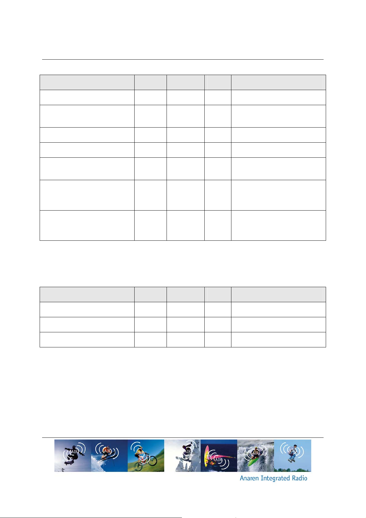
Under no circumstances must the absolute maximum ratings given in Table 1 be violated.
Stress exceeding one or more of the limiting values may cause permanent damage to the
device.
Caution!
ESD sensitive device. Precaution should be
used when handling the device in order to
prevent permanent damage.
Page 19
A85xxE24A91 – Users Manual Page 19 of 28
A
A
Release Date: Dec 1
Parameter Min Max Unit Condition/Note
Supply Voltage (Vdd) -0.3 3.6 V
st
2010
Voltage on any digital pin -0.3 Vdd+ 0.3,
max 3.6
RF input power 0 dBm
Storage Temperature -50 150 ˚C
Solder reflow temperature 260 ˚C According to IPC/JEDEC J-
ESD <500 V
ESD 400 V
Table 1 Absolute Maximum Ratings
V
STD-020D
ccording to JEDEC STD 22,
method A114, Human body
model
ccording to JEDEC STD 22,
C101C, Charged Device
Model (CDM)
4.2. Operating Conditions
Parameter Min Max Unit Condition/Note
Supply Voltage (Vdd) 2.2 3.6 V
Supply Voltage IOVdd 1.8 3.6 V
Temperature Range -40 +85 ˚C
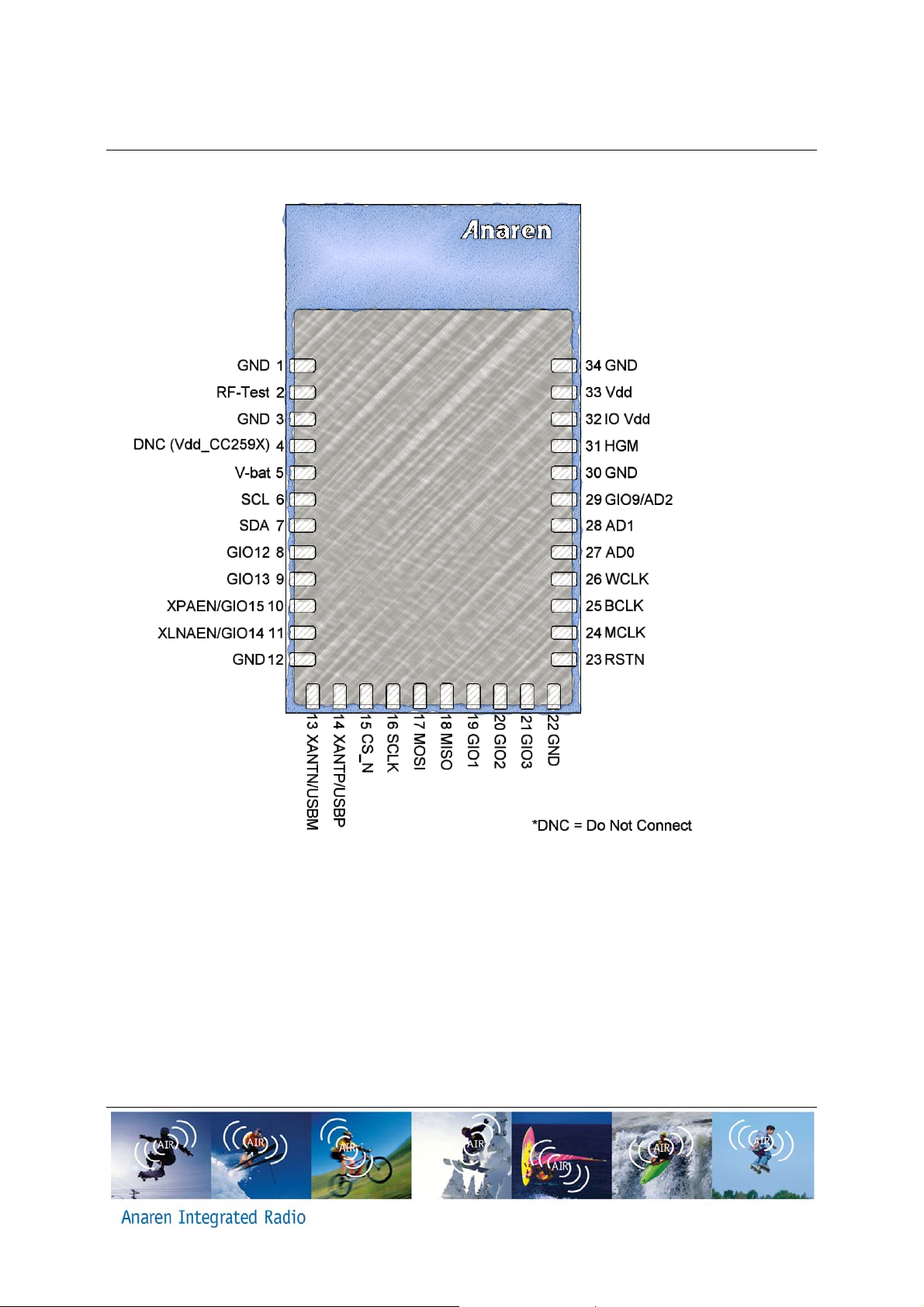
4.3. Pin Out
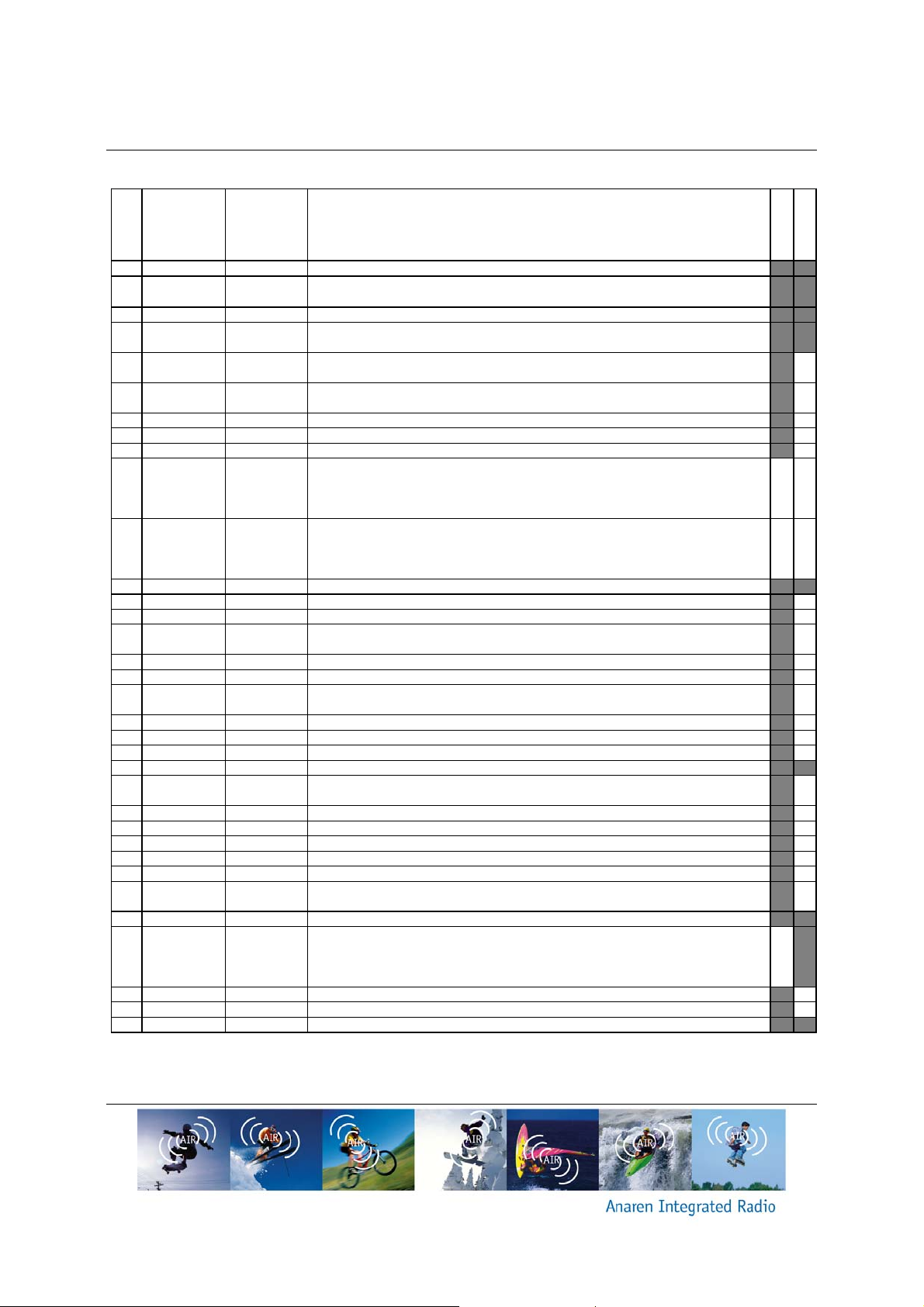
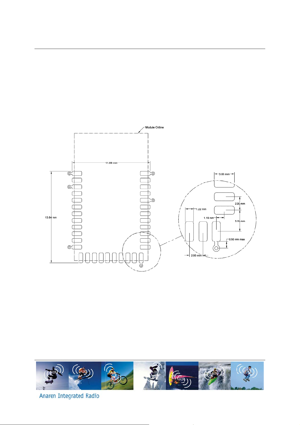
The A85xxE24Axx radio’s share a common pin-out and foot print, thus enabling the use of the
same application PCB layout for US/Europe and low power (short range) versus higher power
(long range). Below the footprint is shown.
Page 20
Page 20 of 28 A85xxE24A91 – Users Manual
Release Date: Dec 1
st
2010
Figure 4 Module pin-out view
Page 21
A85xxE24A91 – Users Manual Page 21 of 28
Release Date: Dec 1
st
2010
Pin Name Pin Type Description
Pin Number
1 GND Common
DNC (RF -
2
Test)
3 GND Common
4 AVdd_CC259x
5 VBAT Analog Input
6 SCL, GIO10 Digital I/O
7 SDA, GI O11 Digital I/O Digital I/O1 I2C master data line. Must be connected to external pull-up, General-purpose 33
8 GIO12 Digital I/O General-purpose digital I/O pin 12 34
9 GIO13 Digital I/O General-purpose digital I/O pin 13 35
10 XPAEN/PAEN Digital Out
11 XLN AEN/EN Digital Out
12 GND Common
13 XANTN Digital I/O Do Not Connect (future antenna diversity control or USB interface) 1
14 XANTP Digital I/O Do Not Connect (future antenna diversity control or USB interface) 2
15 CS_N
16 SCLK Digital I/O Serial SPI configuration interface, clock input/output 4
17 MOSI Digital I/O Serial SPI configuration interface, master data input, slave data output 5
18 MISO, GIO0 Digital I/O
19 GIO1 Digital I/O General-purpose digital I/O pin 1, Configurable with PurePath™ Wireless Configurator 7
20 GIO2 Digital I/O General-purpose digital I/O pin 2 8
21 GIO3 Digital I/O General-purpose digital I/O pin 3, Configurable with PurePath™ Wireless Configurator 9
22 GND Common
23 RSTN
24 MCLK Digital I/O Digital I/O1 Master clock output for external audio devices (GIO4). 13
25 BCLK Digital I/O Digital I/O1 I 2 S/DSP audio interface bit clock (in/out) (GIO5). 14
26 WCLK Digital I/O Digital I/O1 I2S/DSP audio interface word clock (in/out) (GIO6). 15
27 AD0 Digital I/O Digital I/O1 I2S/DSP audio interface data line 0 (in/out) (GIO7). 16
28 AD1 Digital I/O Digital I/O1 I2S/DSP audio interface data line 1 (in/out) (GIO8). 17
29 AD2, GIO9 Digital I/O
30 GND Common
31 HGM Digital Input
32 IOVDD Power (I/O Digital power supply for the digital core, GIO's SPI, I2C and I2S (1.8V to 3.6V) 10
33 AVDD Power Analog power supply connection for the Radio and PA/LNA (2.0V to 3.6V) 20
34 GND Common
Power/Decoup
ling
Digital Input
(Pull-up)
Digital Input
(Pull-up)
Connecting this pin to anything will significantly affect the performance of the module and
may
This pin should not be used unless deemed necessary in particular noisy power supply
environments, See "power supply consideration" section for more information
Battery voltage supervisor (threshold level programmable by external resistor to positive
battery terminal)
I2C master clock line. Must be connected to external pull-up, General-purpose digital I/O
pin 10
The CC85xx asserts this pin high to turn on the CC259x power amplifier for transmit. The
pin can be used to detect the radio state to synchronize other system events e.g. to
smooth out power consumption or minimize noise injection. A high indicates that the PA
is on. At no time will both XPAEN and XLN AEN be high at the same time.
The CC85xx asserts this pin high to turn on the CC259x low noise amplifier. The pin can
be used to detect the radio state to synchronize other system events e.g. to turn of
noise/switching sources for better sensitivity. At no time will both XPAEN a nd XLN AEN
be high at the same time.
Serial SPI configuration interface, active low chip select 3
Serial SPI configuration interface, master data output, slave data input GIO0 output when
CS_N is deasserted. General-purpose digital I/O pin 0
Active-low device reset 11
Digital I/O2 I2S/DSP audio interface data line 2 (in/out), Configurable with PurePath™
Wireless Configurator
Digital control pin. HGM=1 ? CC259x LNA is in High Gain M ode (~10dB gain),
HGM=0 ? CC259x LNA is in Low Gain Mode (~0dB gain). Can be used to avoid
overdriving the receiver in case the transmitter is in very close proximity to the receiver,
otherwise do not connect.
the end users right, under FCC, to operate the module
void
CC259x Pin
CC85xx Pin
29
32
536
638
6
19
7
Table 2 pin-out table, with references to chip pins
Page 22
Page 2
2
4
e
m
B
a
A85x
R
–
2
4.
of 28
. R
comme
nded L
yout
xE24A91
elease Dat
Users Ma
e: Dec 1
st
nual
010
Figure
5 Recom
ended PC
layout.
Page 23
A85xxE24A91 – Users Manual Page 23 of 28
Release Date: Dec 1
st
2010
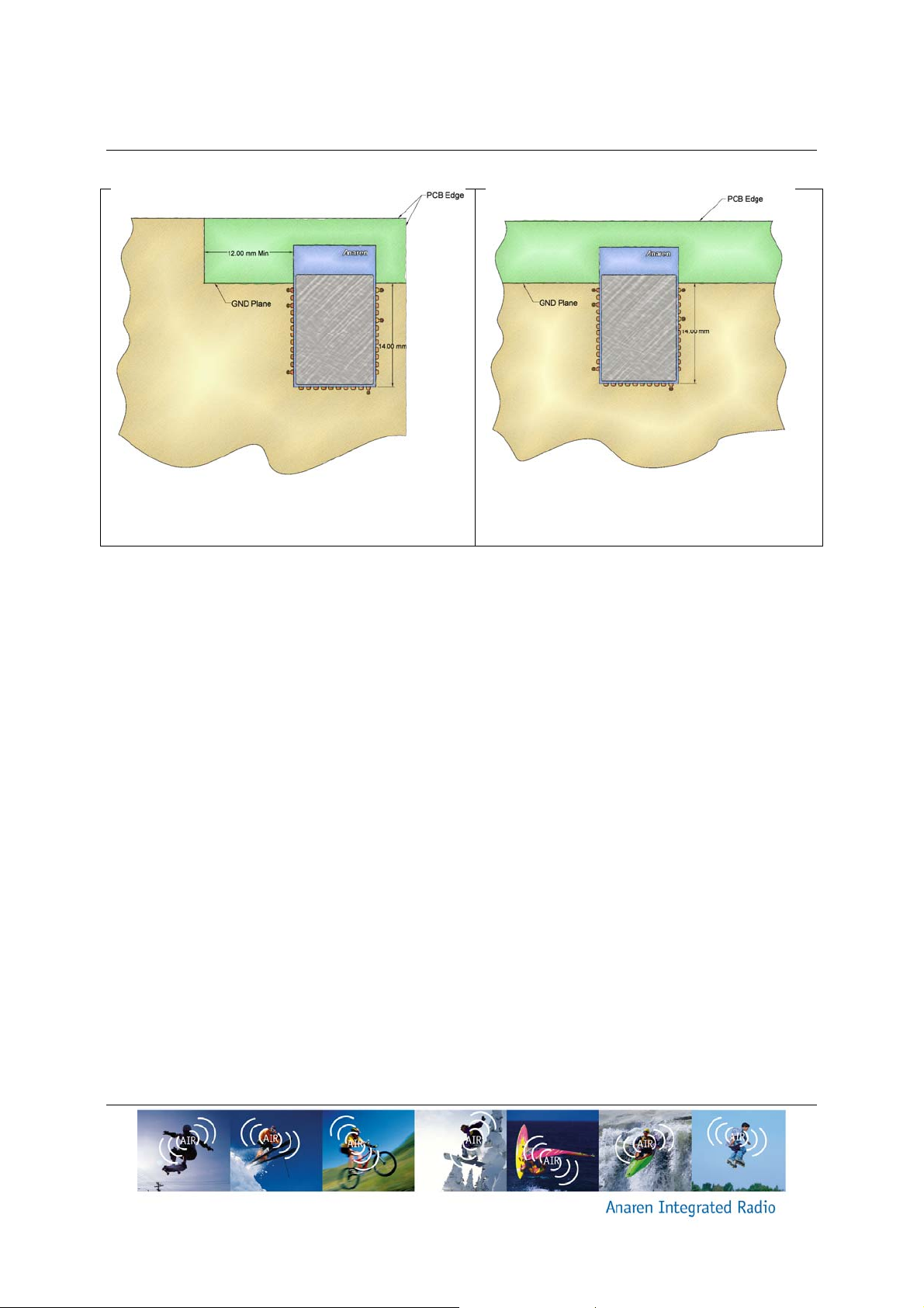
Figure 6 Mounting the module in a corner
Figure 7 Mounting the module along an
edge
4.5. Power Supply Considerations
Noise on the power supply line reduces the sensitivity of a receiver and ca n modulate onto a
transmitters signal, both of which causes a degradation of link quality and hence a reduction in
range.
The A85xxE24Axx radio modules have integral noi se reduction in the supply line from pins 33
(Vdd) and 32 (IOVdd), consisting of ferrite beads and decoupling capacitances. This
arrangement will take care of most supply voltage noise. For optimal performance in particular
noisy environments (switching regulators, motor controls, etc.) it may be necessary to add
additional noise reduction means, which can consist of a low noise LDO or additional LC
filtering.
Pin 4 (AVdd_CC259x) is connected to the modules internal supply line after the ferrite bead and
decoupling capacitors and can be used to probe the noise at module level. The noise level
measured on pin 4 should not exceed 150mVpp when in transmit or receive mode, it may
however exceed this value when not in either trans mit or receive mode or in the trans ition itself
(i.e. it may exceed this if synchronized to the XPAEN and XLNAEN signals.
If the level measured is exceeding the above limit means should be taken to ensure maximum
range:
• Add decoupling capacitance to pin 4 (AVdd_CC259x), 1uF to 2.2µF ceramic capacitor is
suggested (do not use Tantalum).
Page 24
Page 24 of 28 A85xxE24A91 – Users Manual
Release Date: Dec 1
st
2010
• Add decoupling capacitance to pin 33 (AVdd), 1uF to 2.2uF ceramic capacitor is
suggested (do not use Tantalum).
• Add a low noise LDO in the supply line to pin 33 (AVdd) (the TPS731xx low Dropout
Regulator from TI is recommended).
Note that if operated from a battery source there is no need for additional noise reduc tion. Also
note that if the noise source can be synchronized to be off whenever the module is transmitting
or receiving (using XPAEN and XLNAEN) then that will also suffice.
5. Configuration and Programming
The integrator of this module into an application must program the module to match both the
Codec chip used and the human interface methods employed. To do this the integrator must
use the PurePath™ software from Texas Instruments to configure the module
5.1. Calibrating Transmit Power
This power calibration number is an approximate power output value in dBm for the CC85xx
chip – however the modules CC2591 adds an additional 16dB amplification.
The maximum allowed setting to comply with FCC/IC is “0” (which produces 16dBm
output power). Any setting above this voids the end users right to use the equipment.
It can be useful to set a lower power for systems that do not require the full range and thus save
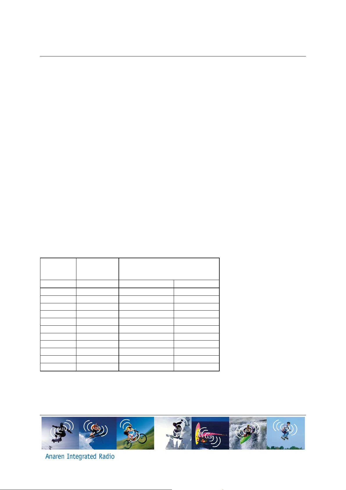
on power consumption. The typical power consumption at 3.3v supply for a A8520E24A91
module is shown below depending on the output power setting.
Output
Power
Setting
# [dBm] Master Slave
0 16 48 18
-1 15 43 18
-2 14 39 17
-3 13 38 17
-4 12 34 16
-5 11 33 16
-6 10 32 15
-7 9 32 15
-8 8 30 15
-9 7 28 15
-10 6 27 15
Actual Output
Power
(Approximate)
Current Consumption [mA] @ 3.3V
AVdd,IOVdd, Ambient
In the PurePath
TM
configurator when creating the application image, in the “Radio” page for both
master and slave the target Tx power must be set to 0 dBm, or lower, (note that this produces
16dBm peak from the module due to CC2591 PA/LNA):
Page 25
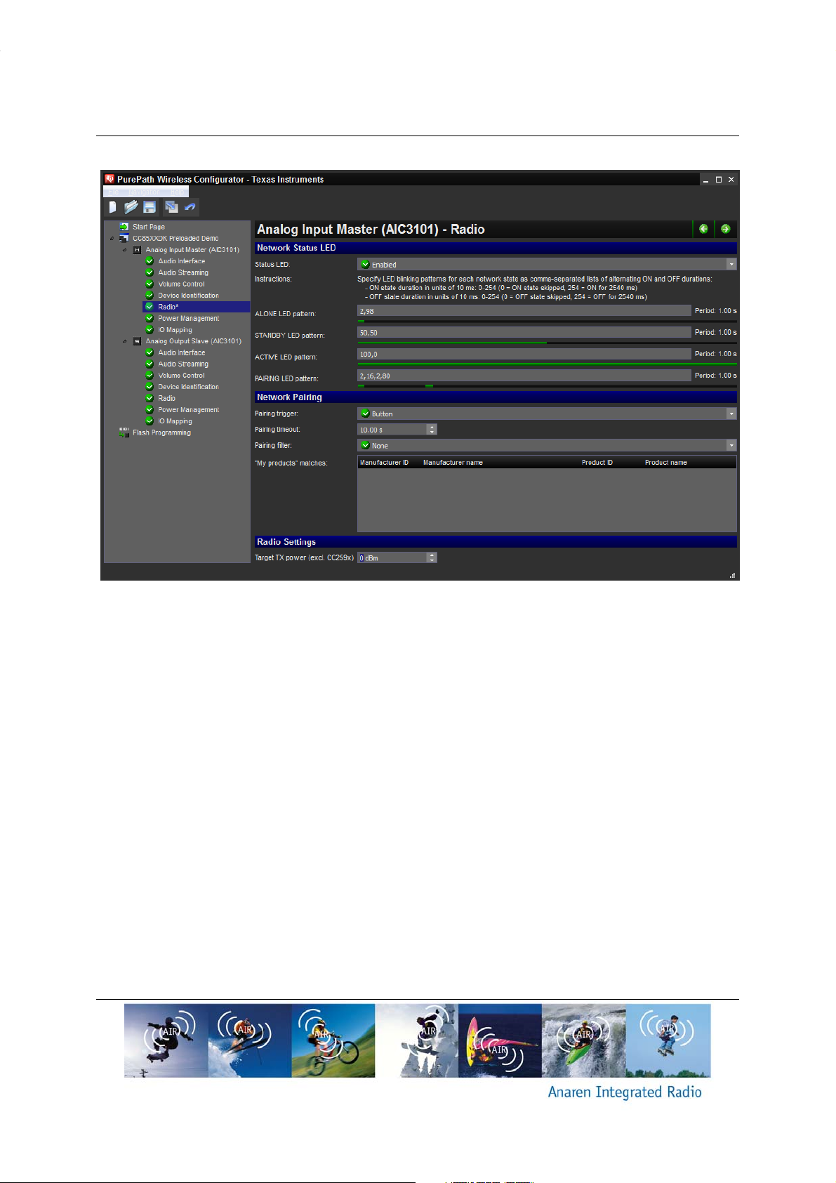
Master
Radio
Page
Slave
Radio
Page
A85xxE24A91 – Users Manual Page 25 of 28
Release Date: Dec 1
st
2010
Target power, set to
0 or lower
Alternatively the power calibration can be done immediately after programming of each module
using the SPI host controller interface, using the
CAL_SET_DATA function. This option is useful if
the same image will be used in multiple equipment, of which some have the power turned down
further than 0 to save current consumption, however it requires a host processor.
5.2. Programming
The desired application image can be programmed into the module either using the PurePath
software and the included CC-Debugger. Or the PurePathTM software can be used to create the
desired image, which is saved and the integrator can use an in-house developed production
programmer to upload the image.
If developing an in-house programmer there are a few things to consider to successfully
program the CC8520 chip. Programming procedure:
// Enter the bootloader
BOOT_RESET();
BL_UNLOCK_SPI();
Check SWR Proceed only if SWR matches required value (Reset device and Restart
programming again)
// Erase the flash
BL_FLASH_MASS_ERASE();
TM
Page 26
Page 26 of 28 A85xxE24A91 – Users Manual
Release Date: Dec 1
st
2010
Check SWR Proceed only if SWR matches required value (Reset device and Restart
programming again)
// For each flash page
for (int n = 0; n < 31; n++) {
// Write page data to the start of the available RAM area
SET_ADDR(0x6000, sw);
WRITE(0x400, data to be programmed into flash page n , sw);
/* While using the image generated by TI- Purepath Wireless Configurator, note that
the entire image file generated by PWC-TI is Intel_hex format. For programming 8520
module use only the data and discard additional data/information */
// Program the page
BL_FLASH_PROG_PAGE(RAM_ADDR = 0x6000, FLASH_ADDR = 0x8000+(n*0x400))
Check SWR Proceed only if SWR matches required value wait till the block is completely
transfered
}
// Verify the flash contents
BL_FLASH_VERIFY(BYTE_COUNT = value read from the HEX file );
/* The flash verify byte count data is 4 byte value stored from location &h 8010
within the image file */
Check SWR Proceed only if SWR matches required value (Reset device and Restart
programming again)
SYS_RESET()
// Done, perform SYS_RESET() to start the application
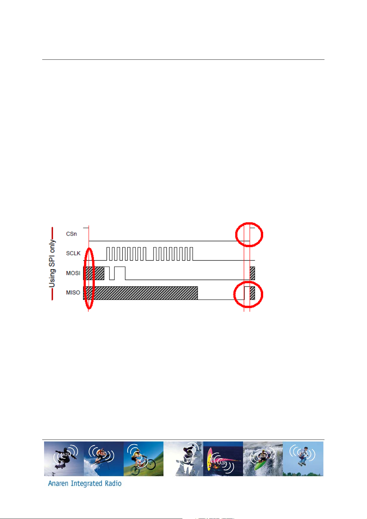
If the status word read fails immediately after execution of BOOT_RESET or BL_UNLOCK_SPI
then it is most likely due to the special SPI requirement during these instructions as MISO must
go low and then high after the SPI clock sequence as shown in the figure below.
If the SPI bus controller is unable to perform this wait, then use the SPI pins as GPIO’s and
manually program the bit sequences as described below for the BOOT_RESET().
Procedure for programming Boot_Reset()
1. Assert CSn Low and then clock the SCL with each negative edge of clock asset the logic
level to high or low on MOSI pin.
2. After sending &H B0 00 on MOSI pin. Wait till MISO pin goes high. Note: Status
check/update is done between MISO and CSn pin going high. If this time is not
sufficient. This will lead to error in SWR read value.
3. One BOOT_RESET is successful then switch to normal SPI operation mode.
Page 27

A85xxE24A91 – Users Manual Page 27 of 28
Release Date: Dec 1
st
2010
HISTORY
Date Author Change Note No./Notes
Aug 8th 2010 Kirkeby Initial Draft
Dec 1st 2010 Kirkeby Initial Release, formatting and content chg.
Dec 13th 2010 Kirkeby Programming and Tx power setting.
Page 28

Thank you for learning more about the
Anaren Integrated Radio (AIR) module line.
If you have additional questions,
need samples, or would like a quote –
please do not hesitate to email the AIR team
Worldwide North America Worldwide
Anaren Microwave, Inc.
6635 Kirkville Road
East Syracuse, NY 13057
Tel: +1 315 432 8909
+1 800 411 6596
Fax: +1 315 432 8970
or contact any of these
authorized distributors of the AIR product line.
Anaren Microwave (Europe), Inc.
12 Somerset House, Suite 16 & 17
Hussar Court, Waterlooville
Hampshire, England P07-7SG
Tel: +44 2392 232392
Fax: +44 2392 251369
Anaren Communication Suzhou Co. Ltd.
No. 5 Chun Hui Road
Wei Ting, Suzhou Industrial Park
Suzhou 215122, PR China
Tel: +86 512 6287 6400
Fax: +86 512 6274 9283
 Loading...