

Analog Microelectronics AME8816CEHAADJ, AME8816BEHAADJ, AME8816BEDVADJ, AME8816AEHA500, AME8816AEHA475 Datasheet
...
AME, Inc.
AME8816
nn
n General Description
nn
The AME8816 family of positive, linear regulators feature low quiescent current (45µA typ.) with low dropout
voltage, making them ideal for battery applications.
Output voltages are set at the factory and trimmed to
1.5% accuracy.
These rugged devices have both Thermal Shutdown,
and Current Fold-back to prevent device failure under
the "Worst" of operating conditions.
In applications requiring a low noise, regulated supply,
place a 1000pF capacitor between Bypass and Ground.
The AME8816 is stable with an output capacitance of
4.7µF or greater .
nn
n Features
nn
1.5A CMOS LDO
nn
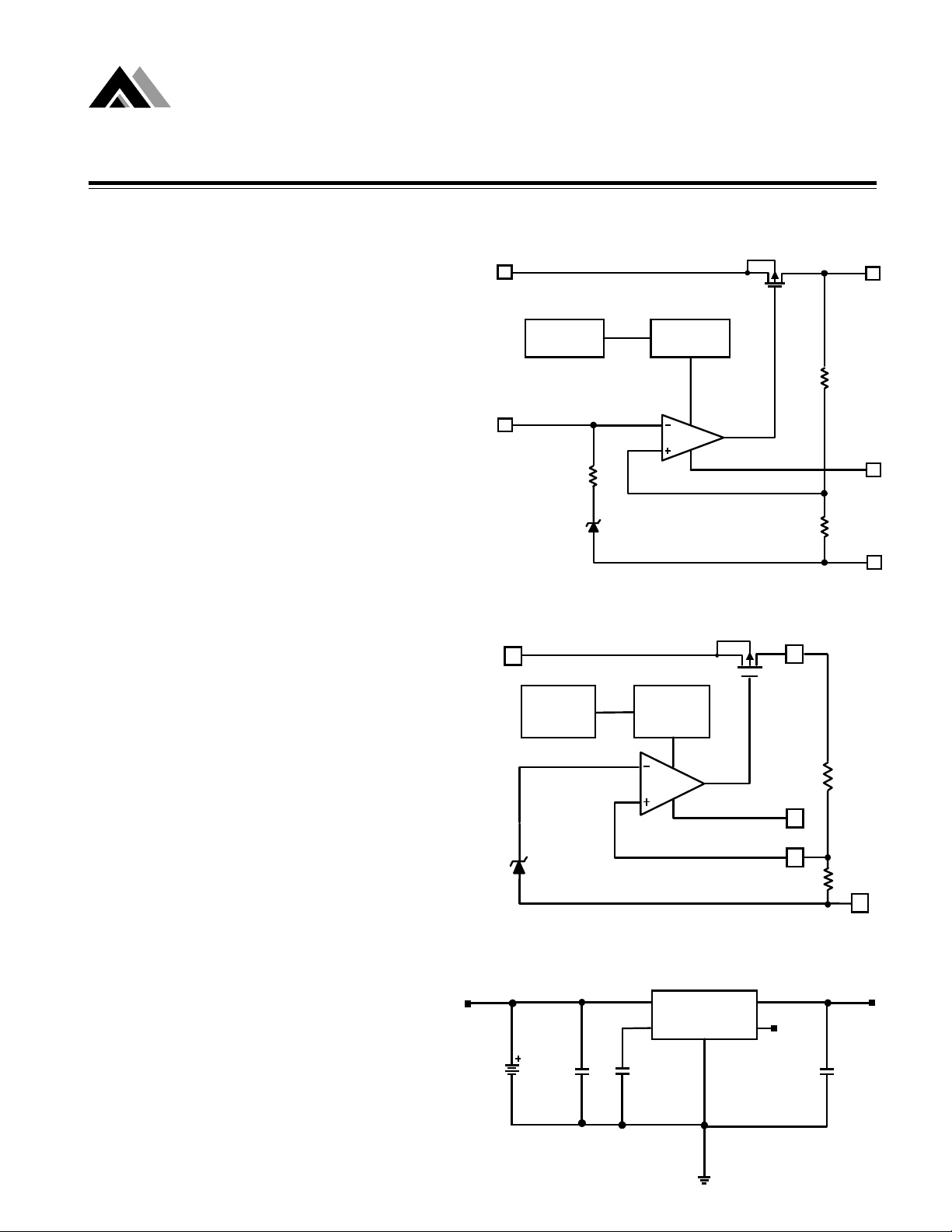
nFunctional Block Diagram
nn
(Fixed Versions)
Overcurrent
Shutdown
BYPASS
1.242V
nn
nFunctional Block Diagram
nn
Thermal
Shutdown
AMP
OUTIN
R1
EN
R2
GND
l Very Low Dropout Voltage
l Guaranteed 1.5A Output
l Accurate to within 1.5%
l 45µA Quiescent Current Typically
l Over-Temperature Shutdown
l Current Limiting
l Short Circuit Current Fold-back
l Noise Reduction Bypass Capacitor (Fixed
Versions)
l Power-Saving Shutdown Mode
l Space-Saving DDPAK-5 Package
l 6 Factory Pre-set Output Voltages
l Low Temperature Coef ficient
l Adjustable Version
nn
n Applications
nn
l Instrumentation
l Portable Electronics
l Wireless Devices
l PC Peripherals
l Battery Powered Widgets
(Adjustable Version)
IN
Overcurrent
Shutdown
1.242V
nn
n T ypical Application
nn
IN
C1
5V
1µF
C2
1nF
Thermal
Shutdown
AMP
IN
BYP
AME8816
OUT
GND
EN
OUT
EN
ADJ
R1
(external)
R2
(external)
GND
OUT
C3
4.7µ
F
1
AME, Inc.
AME8816
nn
n Pin Configuration
nn
AME8816
AEDVXXX
YYWW
12345
TO-263(DDPAK-5) Top View
1. EN
2. V
IN
3. GND
4. V
OUT
5. BYP
AME8816
BEDV ADJ
YYWW
12345
SO-8 Top View
1.5A CMOS LDO
1. EN
2. V
IN
3. GND
4. V
OUT
5. ADJ
8
7
6
5
1. ADJ
2. GND
3. GND
4. EN
5. V
IN
6. GND
7. GND
8. V
OUT
1
O
8
2. GND
1
O
3. GND
1. BYP
2
8816
AEHAXXX
3
4
YYWW
7
6
4. EN
5. V
IN
6. GND
5
7. GND
8. V
OUT
2
3
4
8816
BEHAADJ
YYWW
1. EN
1
2
O
8816
CEHAADJ
3
4
YYWW
8
2. V
IN
3. V
7
6
OUT
4. ADJ
5. GND
6. GND
7. GND
5
8. GND
2
AME, Inc.
AME8816
nnnn
AME8816 Ordering Information
1.5A CMOS LDO
Package Type
V
OUT
DDPAK-5 SO-8
1.50 AM E 8816A EDV150 AM E 8816A EHA150
1.80 AM E 8816A EDV180 AM E 8816A EHA180
2.50 AM E 8816A EDV250 AM E 8816A EHA250
3.30 AM E 8816A EDV330 AM E 8816A EHA330
4.75 AM E 8816A EDV475 AM E 8816A EHA475
5.00 AM E 8816A EDV500 AM E 8816A EHA500
ADJ AME8816B EDVA DJ AM E 8816B EHAA DJ
ADJ AM E 8816CE HA A DJ
Please c ons ult A ME sal es office or authorized Rep./ Distr. F or ot her out put voltage and pack age t ype or pinout
availabili t y.
3
AME, Inc.
AME8816
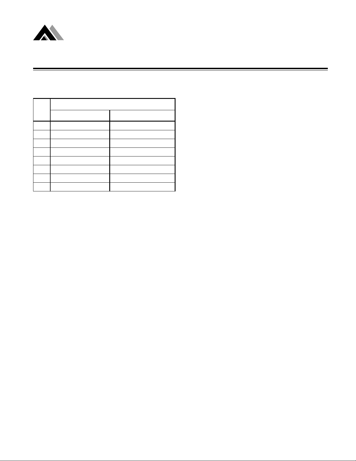
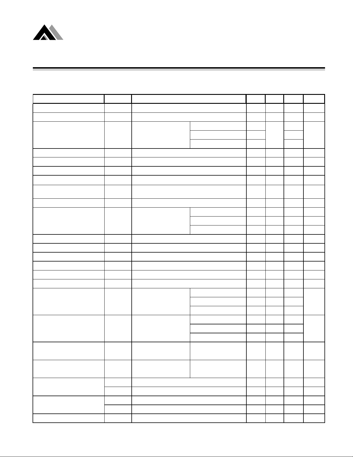
Absolute Maximum Ratings:
nnnn
Parameter Maximum Unit
Inpu t Vo l ta ge 8 V
Output Current
Output V olt age GND - 0.3 to V
ESD Class i fic at i on B
Caution: S t res s above the lis t ed abs olut e m aximum rati ng may c aus e permanent damage t o t he device.
Recommended operating Conditions:
nnnn
Parameter Rating Un it
Am bient Temperature Range -40 to +85
PD / (VIN - VO)
+ 0.3 V
IN
1.5A CMOS LDO
mA
o
C
Junction Temperature -40 to +125
Thermal Information
nnnn
Parame ter
TO-263 (DDPAK -5) 5
Thermal Resistance (
Internal Power Diss ipat ion (P
o
(∆T = 100
Max im um Junct i on Temperature
Max im um Lead Temperature ( 10 Sec)
C)*
)
θ
jc
)
D
SO-8 20**
TO-263 (DDPAK -5) 3.00
SO-8 2.50
o
C
Maximum Unit
o
C / W
W
150
300
o
C
o
C
* As s um ing a heat s ink c apable of twice t imes (
** Estimated
4
)
θ
jc
AME, Inc.
AME8816
nn
n Electrical Specifications
nn
V
= V
IN
Input Voltage V
Output Voltage Accuracy V
Dropout Voltage V
Output C urrent I
Current Limit I
Short Circuit Current I
Quiescent Current I
M inimun Load Current
(For ADJ Option)
Ground Pin Current I
Line Regulation RE G
Load Regulation RE G
+2V, VEN = VIN, TA = 25oC unless otherwise noted
O(nom)
Para mete r Symb ol Min Typ Ma x Units
IN
O
DROPOUT
O
LIM
SC
Q
I
MIN
GND
LINE
LOAD
IO=1.5A
V
O=VONOM
IO=1mA
V
IN=VO
Te st Condition
V
= VEHmin, IO=1mA
EN
-2.0%
V
O
V
O
V
O
I
O
=1m A to 1.5A
I
O
+1 to VO+2
I
=1m A to 1.5A
O
1.5V < V
2.0V <V
>1.2V
>1.2V
<0.4V
=0mA
Note 1 7 V
-1.5 1. 5 %
<= 2.0V 1300
O(NOM)
<= 2.8V 800
O(NOM)
2.8V <V
O(NOM)
1500 m A
1500 2000 m A
< 2.0V -0.15 0.15 %
V
O
4.0 > V
>= 2.0V -0.1 0.02 0.1 %
O
4.0V <= V
O
-0.4 0. 4 %
1.5A CMOS LDO
See
chart
750 m A
1mA
-1 0. 2 1 %
Over Temerature Shut down OTS 150
Over Temerature Hys terisis OTH 30
Temperature Coefficient TC 30
V
O
AD J Input Bias C urrent I
AD J Reference V oltage V
ADJ
REF
V
= 5V , V
IN
= 1.24 2V
ADJ
1.223 1.242 1.261 V
f=1kHz 50
I
=100mA
Pow er Supply Rejec tion
Pow er Supply Rejec tion
PS RR f=10kHz 20 dB
PS RR f=10kHz 55 dB
Output V oltage Nois e eN
O
=4.7µF ceramic
C
O
I
=100mA
O
=4.7µF ceramic
C
O
=0.01µF
C
BY P
f=10Hz t o 100k Hz
I
=10mA ,C
O
BY P
=0µF
f=100kHz 15
f=1kHz 75
f=100kHz 30
Co=4.7µF30
600
45 70
45
1
mV
µ
µ
o
o
ppm /
µ
Vrms
µ
A
A
C
C
o
C
A
Output V oltage Nois e eN
EN Input Threshold
EN Input Bias Current
Shut down S upply Current I
Note1.V
Note2.V
IN(min)=VOUT+VDROPOUT
O(nom) :
nom inal output voltage of fixed version
V
V
I
EH
I
EL
SD
EH
EL
f=10Hz t o 100k Hz
I
=10mA ,C
O
BY P
=0.01µF
V
V
= 5V , VO=0V, VEN=0V
IN
VIN= 7V
=0V, VIN= 7V
EN
Co=4.7µF30
Vrms
µ
2.0 Vin V
00.4V
0.1
0.5
0.5 2
A
µ
A
µ
A
µ
5

AME, Inc.
AME8816
nn
n Detailed Description
nn
The AME8816 family of CMOS regulators contain a
PMOS pass transistor, voltage reference, error amplifier ,
over-current protection, and thermal shutdown.
The P-channel pass transistor receives data from the
error amplifier, over-current shutdown, and thermal protection circuits. During normal operation, the error amplifier compares the output voltage to a precision reference. Over-current and Thermal shutdown circuits become active when the junction temperature exceeds
140oC, or the current exceeds 2.2A. During thermal
shutdown, the output voltage remains low. Normal operation is restored when the junction temperature drops
below 120oC.
The AME8816 behaves like a current source when the
load reaches 2.2A. However, if the load impedance
drops below 0.3 ohms, the current drops back to 600mA
to prevent excessive power dissipation. Normal operation is restored when the load resistance exceeds
0.75 ohms.
1.5A CMOS LDO
All capacitors should be placed in close proximity to
the pins. A "Quiet" ground termination is desirable.
This can be achieved with a "Star" connection.
nn
n Enable
nn
When pulled low, the PMOS pass transistor shuts off,
and all internal circuits are powered down. In this state,
the quiescent current is less than 1µA. This pin behaves
much like an electronic switch.
100Kohm resistor is necessary between V
EN pin when VEN is higher than V
Note: There is no internal pull-up for EN PIN.
nn
n Adjustable Version
nn
The adjustable version uses external feedback resistors
to generate an output voltage anywhere from 1.5V
to 5.0V . V adj is trimmed to 1.242V and VOUT is given by
the equation:
IN.
source and
EN
nn
n External Capacitors
nn
The AME8816 is stable with an output capacitor to ground
of 4.7µF or greater . Ceramic capacitors have the lowest
ESR, and will offer the best AC performance. Conversely ,
Aluminum Electrolytic capacitors exhibit the highest
ESR, resulting in the poorest AC response. Unfortunately ,
large value ceramic capacitors are comparatively expensive. One option is to parallel a 0.1µF ceramic capacitor
with a 10µF Aluminum Electrolytic. The benefit is low
ESR, high capacitance, and low overall cost.
A second capacitor is recommended between the input
and ground to stabilize Vin. The input capacitor should
be at least 0.1µF to have a beneficial effect.
A third capacitor can be connected between the BYPASS pin and GND. This capacitor can be a low cost
Polyester Film variety between the value of 0.001 ~
0.01µF. A larger capacitor improves the AC ripple re-
jection, but also makes the output come up slowly . This
"Soft" turn-on is desirable in some applications to limit
turn-on surges.
VOUT = V adj ( 1 + R1 / R2 )
Feedback resistors R1 and R2 should be high enough to
keep quiescent current low, but increasing R1 + R2
will reduce stability . In general, R1 and R2 in the 10’s of
kΩ will produce adequate stability , given reasonable lay-
out precautions. T o improve stability characteristics, keep
6

AME, Inc.
AME8816
Dropout Voltage vs. I
1.2
1
0.8
0.6
0.4
Dropout Voltage (V)
0.2
0
0 0.3 0.6 0.9 1.2 1.5 1.8
Quiescent Current vs. Temperature
41
39
37
35
33
(uA)
31
29
27
Quiescent Current @ 5V
25
-45 -5 25 55 85 115
I
(A)
LOAD
Temperature (0C)
V
OUT
LOAD
=
1.5
1.8
2.0
2.1
2.8
3.3
1.5A CMOS LDO
Dropout Voltage vs. V
1
I
=1.5A
LOAD
0.8
0.6
I
=1.0A
0.4
0.2
Dropout Voltage (V)
0
02468
Ground Current vs. V
50
45
A)
40
µ
µµ
µ
35
30
25
20
Ground Current (
15
10
2345678
LOAD
V
OUT
VIN (V)
(V)
I
OUT
V
OUT
OUT
I
=0.5A
LOAD
IN
= 140mA
= 1.5V
Ground Current vs. Load Current
38.5
38
A)
µ
µµ
µ
37.5
37
36.5
36
35.5
Ground Current (
35
34.5
0 0.25 0.5 0.75 1 1.25 1.5
Load Current (mA)
VIN = 2.5V
V
= 1.5V
OUT
7

AME, Inc.
AME8816
V
vs. Temperature (2.5V)
2.500
2.495
2.490
2.485
2.480
Output Voltage (V)
2.475
Dropout Voltage vs. Load Current
Dropout Voltage @
OUT
-45-5255585115
Temperature (0C)
400
350
300
250
200
150
100
1.5A (mV)
50
0
0.3 0.6 0.9 1.2 1.5
(2.5V)
Load Current (A)
1150C
850C
550C
250C
-50C
-450C
1.5A CMOS LDO
Load Regulation vs. Temperature
0.30
0.25
0.20
0.15
0.10
0.05
Load Regulation (%)
0.00
-45 -5 25 55 85 115
Tem pera ture (0C)
AME8816BEHA VADJ vs Temperature
1.244
1.243
1.242
1.241
1.240
1.239
VADJ (V)
1.238
1.237
1.236
1.235
-45 -5 25 55 85 115
Tem perature (0C)
8

AME, Inc.
AME8816
(50mV/DIV)
OUT
V
(2V/DIV)
IN
V
1V/DIV
OUT
1A/DIV V
LOAD
I
Transient Line Response
CIN = 4.7µF
C
= 4.7µF
OUT
T
= TF = 1µS
R
VOUT = 1.5V
Time (20
µµµµ
S/DIV)
Current Limit Response
VIN = 5V
C
= 4.7µF
IN
C
= 4.7µF
OUT
I
LIM
I
SC
Time 1mS/DIV
0V
0V
0A
1.5A CMOS LDO
Load Step 40mA to 1.5A
1A/DIVV
LOAD
I
10mV/DIV
OUT
Time 500
Current Limit Vs. V
3
2.8
2.6
2.4
2.2
2
1.8
1.6
Current Limit (A)
1.4
1.2
1
CIN = 4.7µF
C
= 4.7µF
OUT
V
= 1.8V
OUT
2345678
VIN (V)
S/DIV
µµµµ
CIN = 4.7µF
C
= 4.7µF
OUT
V
= 4.0V
IN
= 1.8V
V
OUT
IN
0A
Short Circuit Current VS. V
1.6
1.4
1.2
0.8
0.6
0.4
0.2
Short Circuit Current (A)
CIN = 4.7µF
C
= 4.7µF
OUT
1
0
2345678
VIN (V)
IN
Overtemperature Shutdown
1A/DIV
OUT
1V/DIV I
OUT
V
Time 100mS/DIV
VIN = 4V
C
= 4.7µF
IN
C
OUT
= 4.7µF
0A
0V
9

AME, Inc.
AME8816
10000
1000
100
ΩΩ
Ω)
10
ESR (Ω
L
C
1
0.1
0.01
0 250 500 750 1000 1250 1500
Stability vs. ESR vs I
Unstable Region
CL=5µF
Stable Region
Untested Region
LOAD
ILOAD (mA)
1.5A CMOS LDO
Stability vs. ESR vs I
10000
1000
100
)
Ω
ΩΩ
Ω
ESR (
L
C
0.01
Unstable Region
CL=2µF
10
1
0.1
0 250 500 750 1000 1250 1500
Stable Region
Untested Region
ILOAD (mA)
LOAD
Stability vs. ESR vs I
10000
1000
)
Ω
ΩΩ
Ω
ESR (
C
0.01
0.001
Unstable Region
100
10
1
L
0.1
Untested Region
0 250 500 750 1000 1250 1500
CL=10µF
Stable Region
ILOAD (mA)
LOAD
10

AME, Inc.
AME8816
nn
n External Resistor Divider Table
nn
R1(kohm) 1.00 2.00 5.00 10.00 20.00 50.00 100.00 200.00 500.00 1000.00
Vout
1.30 21.41 42.83 107.07 214.14 428.28 1070.69
1.35 11.50 23.00 57.50 115.00 230.00 575.00
1.40 7.86 15.72 39.30 78.61 157.22 393.04
1.45 5.97 11.94 29.86 59.71 119.42 298.56 597.55
1.50 4.81 9.63 24.07 48.14 96.28 240.70 481.68 962.79
1.55 4.03 8.06 20.16 40.32 80.65 201.62 403.44 806.49
1.60 3.47 6.94 17.35 34.69 69.39 173.46 347.07 693.85
1.65 3.04 6.09 15.22 30.44 60.88 152.21 304.52 608.82
1.70 2.71 5.42 13.56 27.12 54.24 135.59 271.27 542.36
1.75 2.44 4.89 12.22 24.45 48.90 122.24 244.56 488.98
1.80 2.23 4.45 11.13 22.26 44.52 111.29 222.64 445.16
1.85 2.04 4.09 10.21 20.43 40.86 102.14 204.33 408.55
1.90 1.89 3.78 9.44 18.88 37.75 94.38 188.80 377.51
1.95 1.75 3.51 8.77 17.54 35.08 87.71 175.46 350.85 877.12
2.00 1.64 3.28 8.19 16.39 32.77 81.93 163.88 327.70 819.26
2.05 1.54 3.07 7.69 15.37 30.74 76.86 153.74 307.43 768.56
2.10 1.45 2.90 7.24 14.48 28.95 72.38 144.78 289.51 723.78
2.15 1.37 2.74 6.84 13.68 27.36 68.39 136.81 273.57 683.92
2.20 1.30 2.59 6.48 12.96 25.93 64.82 129.67 259.29 648.23
2.25 1.23 2.46 6.16 12.32 24.64 61.61 123.23 246.43 616.07
2.30 1.17 2.35 5.87 11.74 23.48 58.70 117.41 234.78 586.96
2.35 1.12 2.24 5.60 11.21 22.42 56.05 112.11 224.19 560.47
2.40 1.07 2.15 5.36 10.73 21.45 53.63 107.27 214.51 536.27
2.45 1.03 2.06 5.14 10.28 20.56 51.41 102.83 205.63 514.07
2.50 0.99 1.97 4.94 9.87 19.75 49.36 98.74 197.46 493.64
2.55 0.95 1.90 4.75 9.50 18.99 47.48 94.97 189.91 474.77
2.60 0.91 1.83 4.57 9.15 18.29 45.73 91.47 182.92 457.29 914.58
2.65 0.88 1.76 4.41 8.82 17.64 44.11 88.22 176.42 441.05 882.10
2.70 0.85 1.70 4.26 8.52 17.04 42.59 85.19 170.37 425.93 851.85
2.75 0.82 1.65 4.12 8.24 16.47 41.18 82.37 164.72 411.80 823.61
2.80 0.80 1.59 3.99 7.97 15.94 39.86 79.73 159.44 398.59 797.18
2.85 0.77 1.54 3.86 7.72 15.45 38.62 77.25 154.48 386.19 772.39
2.90 0.75 1.50 3.75 7.49 14.98 37.45 74.92 149.82 374.55 749.10
2.95 0.73 1.45 3.64 7.27 14.54 36.36 72.72 145.43 363.58 727.17
3.00 0.71 1.41 3.53 7.06 14.13 35.32 70.65 141.30 353.24 706.48
3.05 0.69 1.37 3.43 6.87 13.74 34.35 68.70 137.39 343.47 686.95
3.10 0.67 1.34 3.34 6.68 13.37 33.42 66.85 133.69 334.23 668.46
R2(kohm)=(1.242*R1(kohm))/(Vout-1.242)
1.5A CMOS LDO
11

AME, Inc.
AME8816
nn
n External Resistor Divider Table (contd.)
nn
R1(kohm) 1. 00 2. 00 5.00 10. 00 20.00 50.00 100.00 200. 00 500.00 1000. 00
Vout
3.15 0.65 1. 30 3.25 6.51 13.02 32.55 65. 09 130. 19 325.47 650. 94
3.20 0.63 1. 27 3.17 6.34 12.69 31.72 63. 43 126. 86 317.16 634. 32
3.25 0.62 1. 24 3.09 6.19 12.37 30.93 61. 85 123. 71 309.26 618. 53
3.30 0.60 1. 21 3.02 6.03 12.07 30.17 60. 35 120. 70 301.75 603. 50
3.35 0.59 1. 18 2.95 5.89 11.78 29.46 58. 92 117. 84 294.59 589. 18
3.40 0.58 1. 15 2.88 5.76 11.51 28.78 57. 55 115. 11 287.77 575. 53
3.45 0.56 1. 13 2.81 5.63 11.25 28.13 56. 25 112. 50 281.25 562. 50
3.50 0.55 1. 10 2.75 5.50 11.00 27.50 55. 00 110. 01 275.02 550. 04
3.55 0.54 1. 08 2.69 5.38 10.76 26.91 53. 81 107. 63 269.06 538. 13
3.60 0.53 1. 05 2.63 5.27 10.53 26.34 52. 67 105. 34 263.36 526. 72
3.65 0.52 1. 03 2.58 5.16 10.32 25.79 51. 58 103. 16 257.89 515. 78
3.70 0.51 1. 01 2.53 5.05 10.11 25.26 50. 53 101. 06 252.64 505. 29
3.75 0.50 0. 99 2.48 4.95 9. 90 24.76 49.52 99.04 247.61 495. 22
3.80 0.49 0. 97 2.43 4.86 9. 71 24.28 48.55 97.11 242.77 485. 54
3.85 0.48 0. 95 2.38 4.76 9. 52 23.81 47.62 95.25 238.11 476. 23
3.90 0.47 0. 93 2.34 4.67 9. 35 23.36 46.73 93.45 233.63 467. 27
3.95 0.46 0. 92 2.29 4.59 9. 17 22.93 45.86 91.73 229.32 458. 64
4.00 0.45 0. 90 2.25 4.50 9. 01 22.52 45.03 90.07 225.16 450. 33
4.05 0.44 0. 88 2.21 4.42 8. 85 22.12 44.23 88.46 221.15 442. 31
4.10 0.43 0. 87 2.17 4.35 8. 69 21.73 43.46 86.91 217.28 434. 57
4.15 0.43 0. 85 2.14 4.27 8. 54 21.35 42.71 85.42 213.55 427. 10
4.20 0.42 0. 84 2.10 4.20 8. 40 20.99 41.99 83.98 209.94 419. 88
4.25 0.41 0. 83 2.06 4.13 8. 26 20.64 41.29 82.58 206.45 412. 90
4.30 0.41 0. 81 2.03 4.06 8. 12 20.31 40.61 81.23 203.07 406. 15
4.35 0.40 0. 80 2.00 4.00 7. 99 19.98 39.96 79.92 199.81 399. 61
4.40 0.39 0. 79 1.97 3.93 7. 87 19.66 39.33 78.66 196.64 393. 29
4.45 0.39 0. 77 1.94 3.87 7. 74 19.36 38.72 77.43 193.58 387. 16
4.50 0.38 0. 76 1.91 3.81 7. 62 19.06 38.12 76.24 190.61 381. 22
4.55 0.38 0. 75 1.88 3.75 7. 51 18.77 37.55 75.09 187.73 375. 45
4.60 0.37 0. 74 1.85 3.70 7. 40 18.49 36.99 73.97 184.93 369. 86
4.65 0.36 0. 73 1.82 3.64 7. 29 18.22 36.44 72.89 182.22 364. 44
4.70 0.36 0. 72 1.80 3.59 7. 18 17.96 35.92 71.83 179.58 359. 17
4.75 0.35 0. 71 1.77 3.54 7. 08 17.70 35.40 70.81 177.02 354. 05
4.80 0.35 0. 70 1.75 3.49 6. 98 17.45 34.91 69.81 174.54 349. 07
4.85 0.34 0. 69 1.72 3.44 6. 88 17.21 34.42 68.85 172.12 344. 24
4.90 0.34 0. 68 1.70 3.40 6. 79 16.98 33.95 67.91 169.76 339. 53
4.95 0.33 0. 67 1.67 3.35 6. 70 16.75 33.50 66.99 167.48 334. 95
5.00 0.33 0. 66 1.65 3.30 6. 61 16.52 33.05 66.10 165.25 330. 49
R2(kohm)= (1.242*R1(kohm))/ (Vout-1.242)
1.5A CMOS LDO
Note: Small load(greater than 2 mA) is necessary as R1 or R2 is larger than 50 Kohm. Otherwise, output
voltage probably cannot be pulled down to 0 V on disable mode.
12

AME, Inc.
AME8816
nn
n Package Dimension
nn
TO-263 (DDPAK-5)
Top View
Front View
Side View
1.5A CMOS LDO
SYMBO LS
A 10.05 10.31 0.396 0.406
B 8.28 8.53 0.326 0.336
C 4.31 4.57 0.170 0.180
D 0.66 0.91 0.026 0.036
E 1.14 1.40 0.045 0.055
G
H 14.73 15.75 0.580 0.620
K 1.40 1.68 0.000 0.066
L 0.00 0.25 0.055 0.010
M 2.49 2.74 0.000 0.108
N 0.43 0.58 0.098 0.023
P 2.29 2.79 0.017 0.110
R
S 2.41 2.67 0.095 0.105
W
MILLIMETERS INCHES
MIN MAX MIN MAX
1.70 ref 0.067 ref
o
0
o
8
0.25 0.01
o
0
o
8
SO-8
Top View
Front View
Side View
θ
SYMBOLS
A 1.35 1.75 0.053 0.069
A
1
A2
B 0.33 0.51 0.013 0.020
C 0.19 0.25 0.007 0.010
D 4.80 5.00 0.189 0.1970
E 3.80 4.00 0.150 0.157
e
H 5.80 6.20 0.228 0.244
L 0.40 1.27 0.016 0.050
y
θθθθ
MILLIMETERS INCHES
MIN MAX MIN MAX
0.10 0.25 0.004 0.010
1.45 REF 0.057 REF
1.27 BSC 0.050 BSC
-
o
0
0.10
8
o
-
o
0
0.004
o
8
13

www.ame.com.tw
E-Mail: info@ame.com.tw
Life Support Policy:
These products of AME, Inc. are not authorized for use as critical components in life-support devices or
systems, without the express written approval of the president
of AME, Inc.
AME, Inc. reserves the right to make changes in the circuitry and specifications of its devices and
advises its customers to obtain the latest version of relevant information.
AME, Inc. , January 2002
Document: 2013-DS8816-C
U.S. Headquarters Corporate Headquarters
Analog Microelectronics, Inc. AME, Inc.
3100 De La Cruz Blvd. Suite 201 2F, 189 Kang-Chien Road, Nei-Hu Dist.
Santa Clara, CA. 95054-2046 Taipei 114 Taiwan, R.O.C.
Tel : (408) 988-2388 Tel : 886 2 2627-8687
Fax: (408) 988-2489 Fax : 886 2 2659-2989
 Loading...